
BGA 425
Semiconductor Group
Jul-14-1998
1
Si-MMIC-Amplifier
in SIEGET
Æ
25-Technologie
VPS05605
4
2
1
3
Preliminary data
∑
Multifunctional casc. 50
block (LNA / MIX)
∑
Unconditionally stable
∑
Gain |
S
21
|
2
= 18.5 dB at 1.8 GHz (appl.1)
gain |
S
21
|
2
= 22 dB at 1.8 GHz (appl.2)
IP
3out
= +7 dBm at 1.8 GHz (
V
D
=3V,
I
D
=9.5mA)
∑
Noise figure
NF = 2.2 dB at 1.8 GHz
∑
Reverse isolation >28 dB (appl.1) >35 dB (appl.2)
∑
typical device voltage
V
D
= 2 V to 5 V
Tape loading orientation
Circuit Diagram
EHA07371
V
2, 5
4
IN
OUTA
+
3
6
OUTB
1
GND
ESD: Electrostatic discharge sensitive device,
observe handling precaution!
PIN Configuration
Type
Marking Ordering Code
1, Out B
3, Out A
2, GND
Package
BGA 425
4, IN
5, GND
6, +V
BMs
Q62702-G0058
SOT-343
Maximum Ratings
Parameter
Symbol
Value
Unit
Device current
I
D
25
mA
Device voltage
V
D
,+V
V
6
Total power dissipation,
T
S
tbd ∞C
P
tot
150
mW
R
F
input power
P
RFin
-10
dBm
Junction temperature
T
j
150
∞C
Ambient temperature
T
A
-65 ...+150
Storage temperature
T
stg
-65 ...+150
Thermal Resistance
Junction - soldering point
1)
R
thJS
tbd
K/W
1)
T
S
is measured on the ground lead at the soldering point to the pcb
Semiconductor Group
1
1998-11-01
BGA 425
Semiconductor Group
Jul-14-1998
2
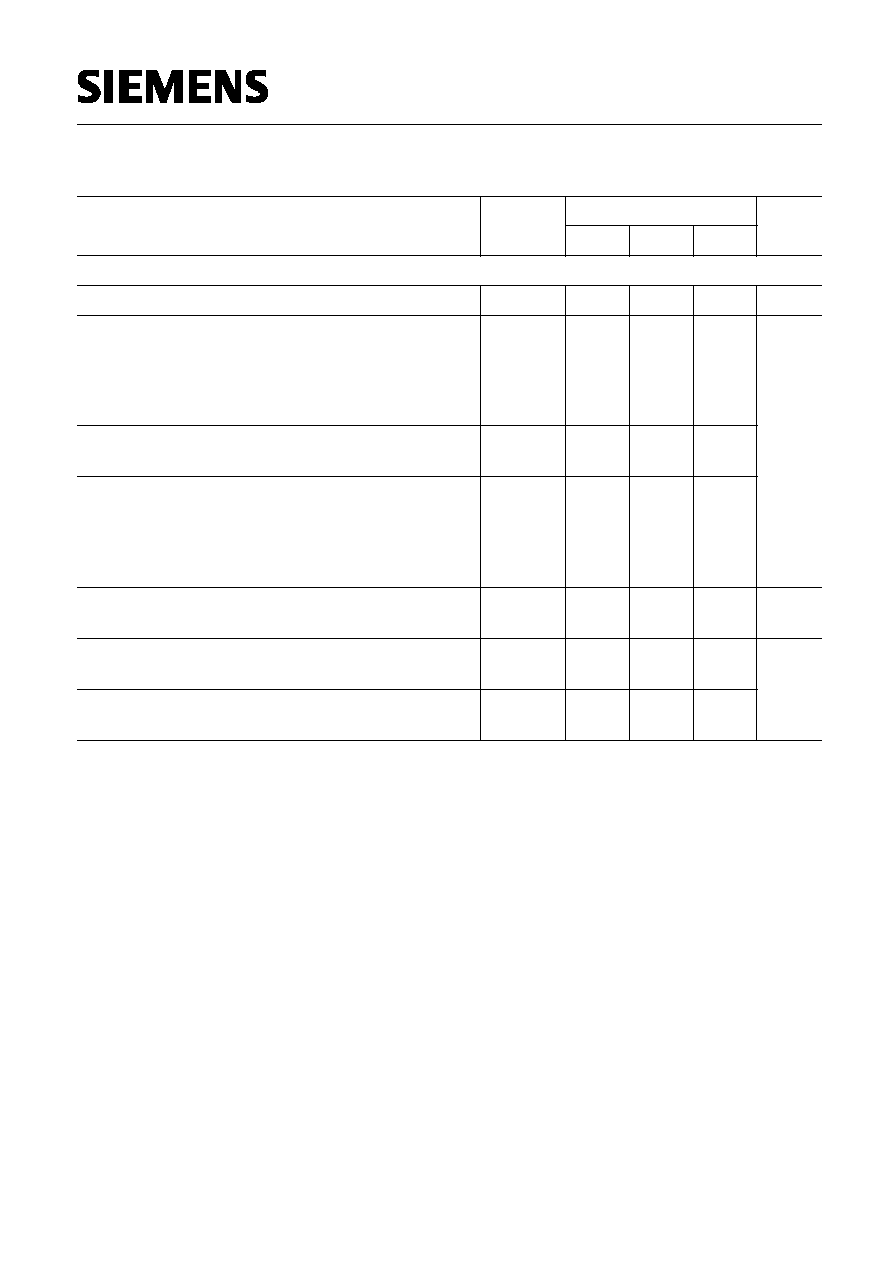
Electrical Characteristics at
T
A
= 25 ∞C, unless otherwise specified.
Parameter
Symbol
Values
Unit
min.
typ.
max.
AC characteristics
V
D
= 3V,
Z
o
= 50
, Testfixture Appl.1
Device current
I
D
8.5
9.5
10.5
mA
Insertion power gain
f = 0.1 GHz
f = 1 GHz
f = 1.8 GHz
|
S
21
|
2
-
-
-
27
22
18.5
-
-
-
dB
Reverse isolation
f = 1.8 GHz
S12
-
28
-
Noise figure
f = 0.1 GHz
f = 1 GHz
f = 1.8 GHz
NF
-
-
-
1.9
2
2.2
-
-
-
Intercept point at the output
f = 1.8 GHz
IP
3out
-
+ 7
-
dBm
Return loss input
f = 1.8 GHz
RL
in
-
>13
-
dB
Return loss output
f = 1.8 GHz
RL
out
-
>7
-
Semiconductor Group
2
1998-11-01
BGA 425
Semiconductor Group
Jul-14-1998
3
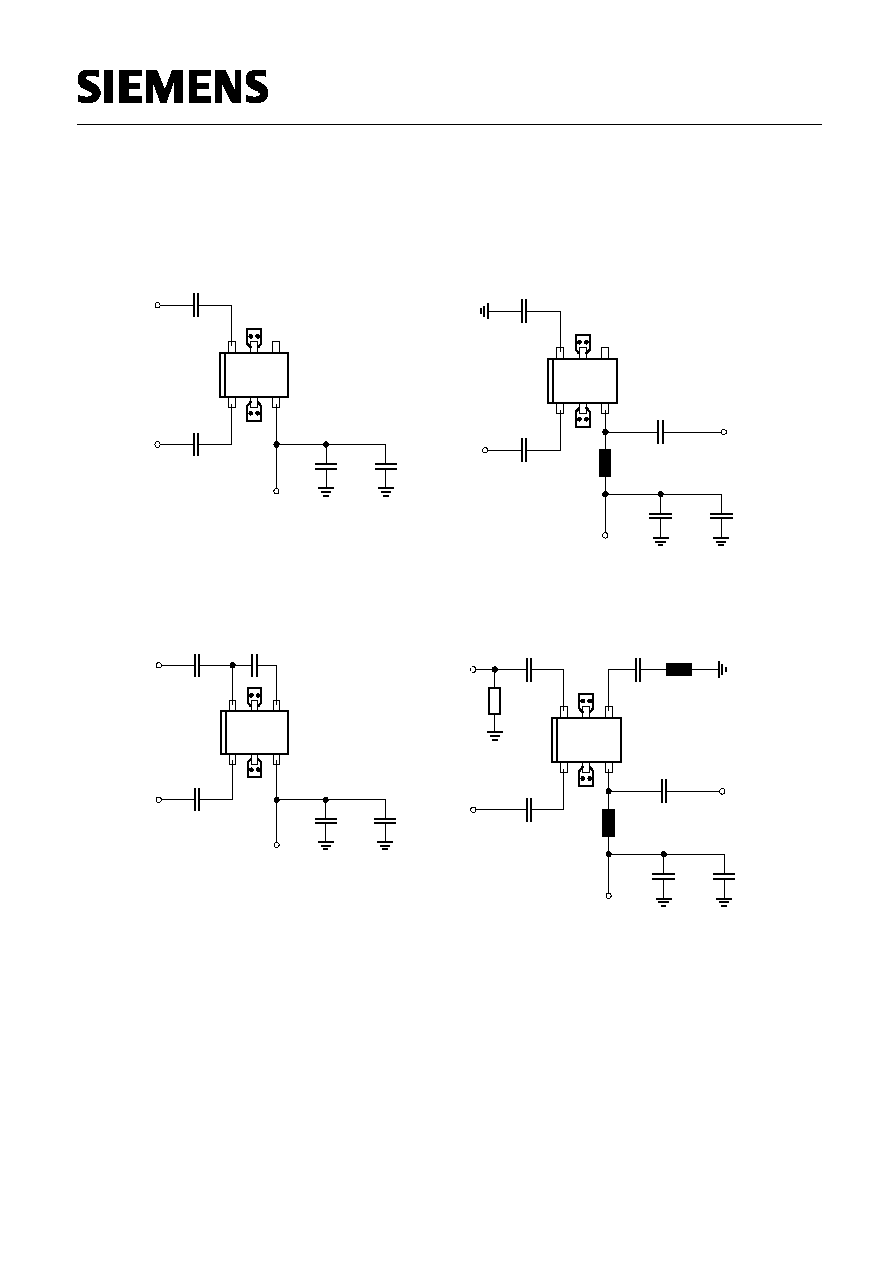
Typical configuration
Application 1 - 3 (LNA)
Application 4 (Mix)
Appl.1
Appl.2
EHA07372
100 pF
100 pF
100 pF
10 nF
+3 V
RF OUT
RF IN
BGA 425
EHA07373
2.2 pF
100 pF
100 pF
10 nF
+3 V
RF OUT
RF IN
100 pF
100 nH
BGA 425
Appl.3
Appl.4
EHA07375
1 nF
100 pF
IF
RF
47 pF
180 nH
LO
33
47 pF
22 nH
10 nF
100 pF
+
V
BGA 425
EHA07374
100 pF
100 pF
100 pF
10 nF
+3 V
RF OUT
RF IN
100 pF
BGA 425
Note: 1) Large-value capacitors should be connected from pin 6 to ground right at the device
to provide a low impedance path! (appl. 1)
2) The use of plated through holes right at pin 2 and 5 is essential for pc-board-applications.
Thin boards are recommended to minimize the parasitic inductance to ground!
3) For more information please see application note 028 and 030.
Semiconductor Group
3
1998-11-01
BGA 425
Semiconductor Group
Jul-14-1998
4
Electrical characteristics at
T
A
= 25 ∞C, unless otherwise specified.
VD = 3 V
Application 1 to 4
Applic.
Insertion Gain
Noise Figure Reverse Isol.
Return Loss
Return Loss
|
S
21
|
2
(dB)
NF (dB)
S12 (dB)
Input
RL
in
(dB) Output
RL
out
(dB)
Frequ. (GHz)
Frequ. (GHz) Frequ. (GHz)
Frequ. (GHz)
Frequ. (GHz)
0.1
1
1.8
0.1 1
1.8 0.1
1
1.8
0.1
1
1.8
0.1
1
1.8
1 (LNA)
27
22
18.5 1.9 2
2.2 46
32
28
19
19
18
10
12
13
2 (LNA)
10
22
22
-
1.9 2.1 35
35
37
13
15
8
5
10
11
*)
3 (LNA)
24
20
16
1.9 2
2.2 34
30
26
8
10
14
15
17
11
4 (MIX)
e.g.: RF = 900 MHz, IF = 100 MHz, VD = 3 V
Conversion gain: 20 dB
Intercept point output: 0 dBm
Noise figure: < 5 dB
LO-power: +3 dBm
*) 2.2 pF by-pass capacitance and 100 nH bias-inductance
Semiconductor Group
4
1998-11-01

BGA 425
Semiconductor Group
Jul-14-1998
5
For linear simulation please use on-wafer measurement data of our T501 chip an add
resistive and capacitive elements, parasitics and package equivalent circuit.
S-Parameters at
T
A
= 25 ∞C
(On-wafer measurement data T501)
f
S
11
S
21
S
12
S
22
GHz
MAG
ANG
MAG
ANG
MAG
ANG
MAG
ANG
T1,
V
CE
= 1.7 V,
I
C
= 4.7 mA
0.1
0.3
0.5
0.7
0.9
1.1
1.3
1.5
1.7
1.9
2.1
2.3
2.5
2.7
2.9
3.1
0.7996
0.8223
0.8294
0.8162
0.81
0.793
0.7884
0.7651
0.7534
0.74
0.7391
0.7335
0.7186
0.7193
0.702
0.6897
-8
-15.5
-26.3
-34.4
-44.5
-52.8
-61.8
-69.1
-75.9
-81.8
-88.4
-96
-98.4
-103.1
-108
-112.6
11.8466
11.9814
11.9702
11.4624
11.1452
10.739
10.3219
9.7368
9.3137
8.8247
8.4426
8.089
7.6674
7.3034
6.7988
6.4921
172.4
169
162.6
156.8
149.5
144.6
138.9
134
130.2
126
121.9
118
115.5
113.2
109.9
107.4
0.0111
0.0126
0.0163
0.019
0.0208
0.0281
0.0332
0.0373
0.0383
0.0404
0.0417
0.0451
0.0465
0.049
0.0492
0.0501
118
90.9
75.9
72.4
64.7
62.4
58.2
54
49.3
45.6
44.1
41.6
40.8
40
37
36.7
0.9942
0.9853
0.9675
0.9529
0.9286
0.9094
0.8842
0.8523
0.8221
0.7939
0.7721
0.7476
0.7339
0.716
0.6885
0.6743
0
-5.7
-9.6
-13.5
-17.2
-20.4
-23.5
-25.9
-28.2
-30.2
-32.7
-34.5
-35.7
-37.3
-38.6
-39.7
T2,
V
CE
= 2.2 V,
I
C
= 4.7 mA
0.1
0.3
0.5
0.7
0.9
1.1
1.3
1.5
1.7
1.9
2.1
2.3
2.5
2.7
2.9
3.1
0.8144
0.8094
0.8251
0.8171
0.7957
0.7952
0.7953
0.767
0.7618
0.7384
0.739
0.7285
0.718
0.7294
0.6955
0.6868
-8.3
-15.3
-25.8
-34.4
-44.9
-52.5
-61.9
-68.6
-75.5
-81.3
-88.7
-95.8
-97.9
-102.9
-107.8
-111.9
11.9941
12.1389
12.1376
11.6229
11.3048
10.8874
10.4735
9.8866
9.4501
8.9757
8.5788
8.2231
7.7991
7.429
6.9444
6.6064
172.1
169
162.7
157
149.7
144.8
139.2
134.3
130.5
126.3
122.1
118.2
115.5
113.4
110
107.6
0.0154
0.01
0.0129
0.0183
0.0227
0.0261
0.0307
0.0325
0.0361
0.0374
0.04
0.0416
0.0463
0.043
0.0468
0.0481
129.2
80.7
76.3
70.8
70.7
64.2
60.7
54
48
49.2
44.3
39.7
40.4
38.8
35.7
34.2
0.985
0.9906
0.9728
0.9557
0.9375
0.9147
0.8916
0.8595
0.8322
0.8019
0.7857
0.7625
0.7467
0.7273
0.7077
0.689
-0.5
-5.6
-0.1
-12.7
-16
-19
-22.4
-24.5
-26.6
-28.6
-30.9
-32.9
-33.7
-35.8
-36.7
-37.6
Semiconductor Group
5
1998-11-01

BGA 425
Semiconductor Group
Jul-14-1998
6
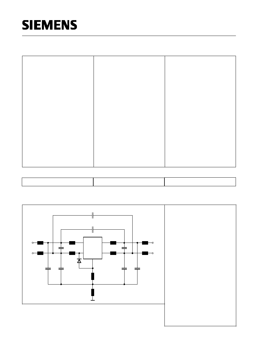
Spice model
T1
T501
T2
T501
R
1
14.5k
R
2
280
R
3
2.4k
170
R
4
R
5
22
R
P1
1k
C
1
2.3pF
C
P1
0.2pF
C
P2
0.2pF
C
P3
0.6pF
C
P4
0.1pF
0.1pF
C
P5
C'-E'-diode T1
EHA07376
3
R
R
1
P1
C
P2
C
1
C
T1
R
2
R
5
P3
C
C
P4
P5
C
R
4
14
13
16
T2
11
12, 15
C'-E'-
including parasitics
Diode
OUTB
OUTA
BGA 425-chip
RF IN
GND
+
V
Semiconductor Group
6
1998-11-01
BGA 425
Semiconductor Group
Jul-14-1998
7
Transistor Chip Data T1 (Berkley-SPICE 2G.6 Syntax) :
BF =
83.23
-
IKF =
0.16493
A
BR =
10.526
-
IKR =
0.25052
A
RB =
15
RE =
1.9289
VJE =
0.70367
V
XTF =
0.3641
-
PTF =
0
deg
MJC =
0.48652
-
CJS =
0
fF
XTB =
0
-
FC =
0.99469
-
IS =
0.21024
aA
VAF =
39.251
V
NE =
1.7763
-
VAR =
34.368
V
NC =
1.3152
-
RBM =
1.3491
CJE =
3.7265
fF
TF =
4.5899
ps
ITF =
1.3364
mA
VJC =
0.99532
V
TR =
1.4935
ns
MJS =
0
-
XTI =
3
-
NF =
1.0405
-
ISE =
15.761
fA
NR =
0.96647
-
ISC =
0.037223
fA
IRB =
0.21215
mA
RC =
0.12691
MJE =
0.37747
-
VTF =
0.19762
V
CJC =
96.941
fF
XCJC =
0.08161
-
VJS =
0.75
V
EG =
1.11
eV
TNOM
300
K
C'-E'-Diode Data (Berkley-SPICE 2G.6 Syntax) :
RS =
20
IS =
2
fA
N =
1.02
-
All parameters are ready to use, no scaling is necessary
Package Equivalent Circuit:
L
BI1
=
0.4
nH
L
BI2
=
nH
0.7
L
BO1
=
0.3
nH
L
BO2
=
nH
0.3
L
EI
=
0.3
nH
L
EO
=
nH
0.1
L
CI1
=
0.4
nH
nH
0.4
L
CI2
=
L
CO1
=
0.3
nH
L
CO2
=
0.3
nH
C
BE1
=
fF
200
C
BE2
=
200
fF
C
CE1
=
200
fF
200
fF
C
CE2
=
C
11
=
5
fF
C
22
=
5
fF
C
12
=
50
fF
C
21
=
50
fF
EHA07377
L
BI2
11
C
BI1
L
BE2
C
BE1
C
BO1
L
BO2
L
OUTA
EI
L
L
EO
12
C
21
C
CI2
L
CI1
L
C
22
CO2
L
L
CO1
CE1
C
CE2
C
OUTB
Chip
14
16
11
13
12, 15
C'-E'-
RF IN
Diode
GND
+
V
BGA 425
Extracted on behalf of SIEMENS Small Signal Semiconductors by
Institut f¸r Mobil-und Satellitentechnik (IMST)
©
1996 SIEMENS AG
Valid up to 3GHz
For examples and ready to use parameters please contact your local Siemens distributor or sales office to
obtain a Siemens CD-ROM or see Internet: http://www.siemens.de/Semiconductor/products/35/35.htm
Semiconductor Group
7
1998-11-01

BGA 425
Semiconductor Group
Jul-14-1998
8
Insertion power gain |
S
21
|
2
=
f (f)
V
D
,
I
D
= parameter
10
-1
10
0
10
1
GHz
f
0
5
10
15
20
25
dB
35
|
S
21
|
2
VD=5V, ID=17.5mA
VD=4V, ID=13.3mA
VD=3V, ID=9.5mA
VD=2V, ID=5.2mA
Noise figure
NF = f (f)
V
D
,
I
D
= parameter
10
-1
10
0
10
1
GHz
f
0.0
0.5
1.0
1.5
2.0
2.5
3.0
3.5
4.0
dB
5.0
NF
VD=5V, ID=17.5mA
VD=3V, ID=9.5mA
Intercept point at the output
IP
3out
=
f (f)
V
D
,
I
D
= parameter
10
-1
10
0
10
1
GHz
f
0
2
4
6
8
10
12
14
16
dBm
20
IP
3out
VD=5V, ID=17.5mA
VD=4V, ID=13,3mA
VD=3V, ID=9.5mA
VD=2V, ID=5.2mA
Semiconductor Group
8
1998-11-01