 | –≠–ª–µ–∫—Ç—Ä–æ–Ω–Ω—ã–π –∫–æ–º–ø–æ–Ω–µ–Ω—Ç: Q62702G63 | –°–∫–∞—á–∞—Ç—å:  PDF PDF  ZIP ZIP |
CGY 96
Siemens Aktiengesellschaft
1
23.07.1998
HL HF PE GaAs
GaAs MMIC
l
Power amplifier for GSM class 4 phones
l
3.2 W (35dBm) output power at 3.5 V
l
Overall power added efficiency 50 %
l
Fully integrated 3 stage amplifier
l
Power ramp control
l
Input matched to 50 ohms, simple output match
ESD: Electrostatic discharge sensitive device,
observe handling precautions!
Type
Marking
Ordering code
(taped)
Package
CGY 96
CGY 96
Q62702G63
MW 16
Maximum ratings
Characteristics
Symbol
max. Value
Unit
Positive supply voltage
VD
9
V
Supply current
ID
4
A
Channel temperature
TCh
150
∞C
Storage temperature
Tstg
-55...+150
∞C
Pulse peak power dissipation
duty cycle 12.5%, ton=0.577ms
PPulse
tbd
W
Total power dissipation
(Ts
80 ∞C)
Ts: Temperature at soldering point
Ptot
tbd
W
Thermal Resistance
Characteristics
Symbol
max. Value
Unit
Channel-soldering point
RthChS
tbd
K/W
Semiconductor Group
1
1998-11-01
CGY 96
Siemens Aktiengesellschaft
2
23.07.1998
HL HF PE GaAs
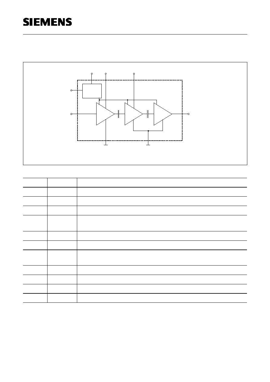
Functional block diagramm:
Pin #
Name
Configuration
1
VD1
Drain voltage 1st stage
2
VD2
Drain voltage 2nd stage
3
n.c.
-
4,5,6
VD3 /
RFout
Drain 3rd stage and RF-output
7
n.c.
-
8
Vcontrol
Control voltage for power ramping
9,10,11,
12
n.c.
-
13
Vneg
negative voltage for current control circuit
14,15
Gnd1
Ground pin 1st stage
16
RFin
RF Input
(17)
GND2
Ground (backside of MW16 package)
current
control circuit
CGY96
VD1(1)
VD2(2)
Vcontrol(8)
VD3/RFout(4,5,6)
GND2(17)
GND1(14,15)
RFin(16)
Vneg(13)
Semiconductor Group
2
1998-11-01

CGY 96
Siemens Aktiengesellschaft
3
23.07.1998
HL HF PE GaAs
Electrical characteristics
(TA = 25∞C, Vneg=-5V, Vcontrol=2.2V; duty cycle 12.5%, ton=577
µ
sec)
Characteristics
Symbol
min
typ
max
Unit
Frequency range
f
880
-
915
MHz
Supply current
Pin=0dBm
I
D
-
1.8
-
A
Supply current neg. voltage gener.
Vaux=3.5V
I
AUX
-
10
-
mA
Gain (small signal)
G
-
40
-
dB
Power gain
Pin=0dBm
G
P
-
35
-
dB
Output Power
Pin=0dBm, Vcontrol=2.0V.....2.5V)
P
OUT
-
35
-
dBm
Overall Power added Efficiency
Pin=0dBm
-
50
-
%
Dynamic range output power
Vcontrol = 0.2...2.2V
-
80
-
dB
Harmonics
Pin=0dBm
H(2f
0
)
H(3f
0
)
H(4f
0
)
-
-
-
-40
-43
-44
-
-
-
dBc
dBc
dBc
Noise Power in RX
(935-960MHz)
Pin=0dBm, Pout=35dBm, 100kHz
RBW
N
RX
-
-81
-
dBm
Stability
all spurious outputs < -60dBc,
VSWR load, all phase angles
-
10 : 1
-
-
Input VSWR
-
1.7 : 1
-
-
Semiconductor Group
3
1998-11-01

CGY 96
Siemens Aktiengesellschaft
4
23.07.1998
HL HF PE GaAs
Output Power and PAE vs. Input Power
(Vd=3.5V, Vcontrol=2.2V, f=900MHz, duty cycle 12.5%, ton=577
µ
s)
Output Power and PAE vs. Control Voltage:
(Vd=3.5V, Pin=0dBm, f=900MHz, duty cycle 12.5%, ton=577
µ
s)
23
24
25
26
27
28
29
30
31
32
33
34
35
36
37
38
-16 -15 -14 -13 -12 -11 -10 -9
-8
-7
-6
-5
-4
-3
-2
-1
0
1
2
3
4
5
6
Pin [dBm]
Po
ut
[d
B
m]
0
5
10
15
20
25
30
35
40
45
50
55
60
65
70
75
PA
E
[%
]
Pout [dBm]
PAE [%]
-60
-50
-40
-30
-20
-10
0
10
20
30
40
0
0,2
0,4
0,6
0,8
1
1,2
1,4
1,6
1,8
2
2,2
2,4
2,6
2,8
3
Vcontrol [V]
Pout [dB
m
]
0
10
20
30
40
50
60
70
80
90
100
PAE [
%
]
Pout [dBm]
PAE [%]
Semiconductor Group
4
1998-11-01
CGY 96
Siemens Aktiengesellschaft
5
23.07.1998
HL HF PE GaAs
Power Gain and Input Return Loss vs. Frequency
(Vd=3.5V, Vcontrol=2.2V, Pin=5dBm, duty cycle 12.5%, ton=577
µ
s)
25,0
26,0
27,0
28,0
29,0
30,0
31,0
32,0
33,0
34,0
35,0
0,880
0,885
0,890
0,895
0,900
0,905
0,910
0,915
Freq [GHz]
Pow
e
rga
i
n [dB
]
-15,0
-14,5
-14,0
-13,5
-13,0
-12,5
-12,0
-11,5
-11,0
-10,5
-10,0
0,880
0,885
0,890
0,895
0,900
0,905
0,910
0,915
Freq [GHz]
I
nput R
e
turn Loss [dB
]
Semiconductor Group
5
1998-11-01
CGY 96
Siemens Aktiengesellschaft
6
23.07.1998
HL HF PE GaAs
Output Power vs. Drain Voltage
(matched for VD=3.5V, Vcontrol=2.2V, Pin=0dBm, duty cycle 12.5%, ton=577
µ
s)
Output Power at different Temperatures
(Vd=3.5V, Vcontrol=2.2V, f=900MHz, duty cycle 12.5%, ton=577
µ
s)
30
31
32
33
34
35
36
37
38
39
40
2,2
2,4
2,6
2,8
3,0
3,2
3,4
3,6
3,8
4,0
4,2
4,4
4,6
4,8
5,0
5,2
VD [V]
Po
t [d
B
m
]
28,0
28,5
29,0
29,5
30,0
30,5
31,0
31,5
32,0
32,5
33,0
33,5
34,0
34,5
35,0
35,5
36,0
-11
-10
-9
-8
-7
-6
-5
-4
-3
-2
-1
0
1
2
3
4
5
6
7
8
Pin [dBm]
P
out
[
d
Bm
]
-20∞C
+20∞C
+70∞C
Semiconductor Group
6
1998-11-01

CGY 96
Siemens Aktiengesellschaft
7
23.07.1998
HL HF PE GaAs
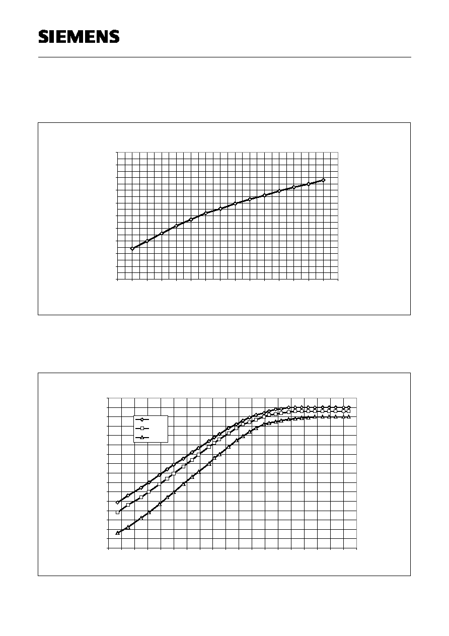
PAE at different Temperatures
(Vd=3.5V, Vcontrol=2.2V, f=900MHz, duty cycle 12.5%, ton=577
µ
s)
0
5
10
15
20
25
30
35
40
45
50
55
-11
-10
-9
-8
-7
-6
-5
-4
-3
-2
-1
0
1
2
3
4
5
6
7
8
Pin [dBm]
PA
E [
%
]
-20∞C
+20∞C
+70∞C
Semiconductor Group
7
1998-11-01

CGY 96
Siemens Aktiengesellschaft
8
23.07.1998
HL HF PE GaAs
CGY 96 Evaluation Board
(Size 34mm x 27mm)
Connections:
∑
Vd
2.7 to 6VDC, pulsed (GSM: 12,5% duty cycle, ton=0.577ms)
∑
Vaux
2.7 to 6VDC
∑
Vcontrol
0.2 to 2.2 VDC (0.2V: min Pout, 2.2V: max Pout)
∑
CLK
5 MHz to 15 MHz (with a 10uH inductor)
or 150 kHz to 250 kHz (with a 100uH inductor instaed of the 10uH)
(rectangular signal, 50% duty, 0 Volt to Vd voltage level)
Power on sequence:
1. continuous clock (CLK) on
2. turn on Vaux ==> check negative voltage at pin#13 (-5......-10V)
3. turn on Vcontrol (may be at the same time as 2)
turn on Drainvoltage Vd
turn on Input Power
Operation without using the negative voltage generator:
Operation without using the on board negative voltage generator is possible. In that case
apply -5....-8 V directly at pin#13 (Vneg-Pin). The decvices in front of pin 13 are not
necessary in that case.
CLK
Vaux
Vc
o
n
C G Y96
T1
D1
C11
C13
R1
2
R11
C14
L11
C1
2
C3
C4
L3
C2
C5
L2
L1
C1
R1
Semiconductor Group
8
1998-11-01

CGY 96
Siemens Aktiengesellschaft
9
23.07.1998
HL HF PE GaAs
Part List:
CGY96
Negative Voltage Generator
L1
L2
L3
C1
C2
C3
C4
C5
R1
33nH
33nH
33nH*
1nF
12pF
10pF**
2.2pF**
1nF
3.3Ohm
D1
T1
L11
C11
C12
C13
C14
R11
R12
BAS40-04W
BC848B
10uH
1nF
1nF
47nF
1nF
3.8kOhm
680Ohm
* 33nH SMD-Inductor for drain3: Part Number BV1250
distribution by
Horst David GmbH, 85375 Neufarn, Germany
Phone-No ..8165/9548-0 , Fax-No ..8165/9548-28
** for maximum efficiency use high quality capacitors for
the output matching: Part Number ACCU-P0603
distribution by
AVX GmbH, 85757 Karlsfeld, Germany
Phone-No ..8131/9004-0
CGY96
Vcontrol
RF IN
Vd
RF OUT
L3
C5
C3
(Vneg)
Vaux
C11
C13
R11
C14
C12
L11
R12
T1
D1.1
D1.2
CLK
C2
C1
L1
L2
R1
VD1
VD2
RFout
Vcon
Vneg
GND1
GND1
RFin
RFout
RFout
C4
Semiconductor Group
9
1998-11-01

CGY 96
Siemens Aktiengesellschaft
10
23.07.1998
HL HF PE GaAs
Published by Siemens AG, Bereich Bauelemente, Vertrieb,
Produkt-Information, Balanstraþe 73, D-81541 M¸nchen
copyright
Siemens AG 1996. All Rights Reserved
As far as patents or other rights of third parties are concerned, liability is only assumed for
components per se, not for applications, processes and circuits implemented within
components or assemblies.
The information describes the type of component and shall not be considered as assured
characteristics.
Terms of delivery and rights to change design reserved.
For questions on technology, delivery and prices please contact the Offices of
Semiconductor Group in Germany or the Siemens Companies and Representatives world-
wide (see address list).
Due to technical requirements components may contain dangerous substances. For
information on the type in question please contact your nearest Siemens Office,
Semiconductor Group.
Siemens AG is an approved CECC manufacturer.
Semiconductor Group
10
1998-11-01