 | –≠–ª–µ–∫—Ç—Ä–æ–Ω–Ω—ã–π –∫–æ–º–ø–æ–Ω–µ–Ω—Ç: Q62702-K8 | –°–∫–∞—á–∞—Ç—å:  PDF PDF  ZIP ZIP |
KOM 2057 L
3fach-Silizium-Fotodiodenzeile
3-Chip Silicon Photodiode Array
Wesentliche Merkmale
q
Speziell geeignet f¸r Anwendungen im
Bereich von 400 nm bis 1100 nm
q
Kurze Schaltzeit (typ. 14 ns)
q
DIL-Plastikbauform
Anwendungen
q
Nachlaufsteuerungen
q
Kantenf¸hrung
q
Positionierung
q
Industrieelektronik
q
"Messen/Steuern/Regeln"
Features
q
Especially suitable for applications from
400 nm to 1100 nm
q
Short switching time (typ. 14 ns)
q
DIL plastic package
Applications
q
Follow-up controls
q
Edge drives
q
Positioning
q
Industrial electronics
q
For control and drive circuits
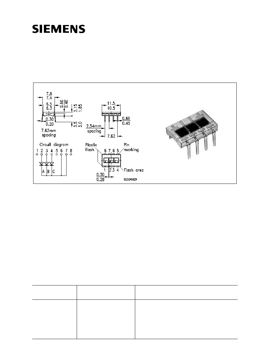
KOM 2057 L
Typ
Type
Bestellnummer
Ordering Code
Geh‰use
Package
KOM 2057 L
Q62702-K8
klares Epoxy
-
Gieþharz, Lˆtspieþe im
7,62-mm-Raster (
3
/
10
"),
Kathodenkennzeichnung: Nase am Lˆtspieþ
transparent epoxy resin, solder leads in
7.62 mm spacing (
3
/
10
"), cathode marking:
projection at solder lead
Maþe in mm, wenn nicht anders angegeben/Dimensions in mm, unless otherwise specified.
feo06429
KOM 2057 L
Grenzwerte
Maximum Ratings
Bezeichnung
Description
Symbol
Symbol
Wert
Value
Einheit
Unit
Betriebs- und Lagertemperatur
Operating and storage temperature range
T
op
;
T
stg
≠ 40 ... + 80
∞
C
Lˆttemperatur (Lˆtstelle 2 mm vom Geh‰use
entfernt bei Lˆtzeit
t
=
3 s)
Soldering temperature in 2 mm distance from
case bottom (
t
=
3 s)
T
S
230
∞
C
Sperrspannung
Reverse voltage
V
R
32
V
Verlustleistung,
T
A
= 25
∞
C
Total power dissipation
P
tot
150
mW
Kennwerte (
T
A
= 25
∞
C, Normlicht A, 2856 K) f¸r jede Einzeldiode
Characteristics (
T
A
= 25
∞
C, standard light A, 2856 K) per single diode
Bezeichnung
Description
Symbol
Symbol
Wert
Value
Einheit
Unit
Fotoempfindlichkeit,
V
R
= 5 V
Spectral sensitivity,
V
R
= 5 V
S
80 (
50)
nA/Ix
Wellenl‰nge der max. Fotoempfindlichkeit
Wavelength of max. sensitivity
S max
880
nm
Spektraler Bereich der Fotoempfindlichkeit
S
= 10 % von
S
max
Spectral range of sensitivity
S
= 10 % of
S
max
400 ... 1100
nm
Bestrahlungsempfindliche Fl‰che
Radiant sensitive area
A
7
mm
2
Abmessung der bestrahlungsempfinlichen
Fl‰che
Dimensions of radiant sensitive area
L
◊
B
L
◊
W
2.65
◊
2.65
mm x mm
Abstand Chipoberfl‰che zu
Geh‰useoberfl‰che
Distance chip front to case surface
H
0.4 ... 0.6
mm
Halbwinkel
Half angle
±
60
Grad
deg.
Dunkelstrom,
V
R
= 10 V
Dark current
I
R
2 (
30)
nA
KOM 2057 L
Spektrale Fotoempfindlichkeit,
= 850 nm
Spectral sensitivity
S
0.62
A/W
Maximale Abweichung der
Fotoempfindlichkeit vom Mittelwert
Max. deviation of the system spectral
sensitivity from the average value
S
±
10
%
Quantenausbeute,
= 850 nm
Quantum yield
0.90
Electrons
Photon
Leerlaufspannung,
E
v
= 1000 Ix
Open-circuit voltage
V
O
365 (
300)
mV
Kurzschluþstrom,
E
v
= 1000 Ix
Short-circuit current
I
SC
80
µ
A
Anstiegszeit/Abfallzeit
Rise and fall time
R
L
= 50
,
V
R
= 10 V;
= 850 nm;
I
P
= 800
µ
A
t
r
,
t
f
14
ns
Durchlaþspannung,
I
F
= 100 mA;
E
= 0
Forward voltage
V
F
1.3
V
Kapazit‰t
Capacitance
V
R
= 0 V
; f
= 1 MHz;
E
= 0
C
0
72
pF
Temperaturkoeffizient von
V
O
Temperature coefficient of
V
O
TC
V
≠2.6
mV/K
Temperaturkoeffizient von
I
P
Temperature coefficient of
I
P
TC
I
0.18
%/K
Rausch‰quivalente
Strahlungsleistung
Noise equivalent power
V
R
= 10 V,
= 850 nm
NEP
4.1
◊
10
≠14
W
Hz
Nachweisgrenze,
V
R
= 10 V,
= 850 nm
Detection limit
D*
6.6
◊
10
12
cm ∑
Hz
W
Kennwerte (
T
A
= 25
∞
C, Normlicht A, 2856 K) f¸r jede Einzeldiode
Characteristics (
T
A
= 25
∞
C, standard light A, 2856 K) per single diode
Bezeichnung
Description
Symbol
Symbol
Wert
Value
Einheit
Unit
KOM 2057 L
Relative spectral sensitivity
S
rel
=
f
(
)
Dark current
I
R
=
f
(
V
R
)
,
E
= 0
Directional characteristics
S
rel
=
f
(
)
Photocurrent
I
P
=
f
(
E
v
);
V
R
= 5 V
Open-circuit voltage
V
O
=
f
(
E
v
)
Capacitance
C
=
f
(
V
R
),
f
= 1 MHz,
E
= 0
Total power dissipation
P
tot
=
f
(
T
A
)
Dark current
I
R
=
f
(
T
A
),
V
R
= 10 V
, E
= 0