GaAs FET
CLY 2
________________________________________________________________________________________________________
Siemens Aktiengesellschaft
pg. 1/77
17.12.96
HL EH PD 21
D a t a s h e e t
* Power amplifier for mobile phones
* For frequencies up to 3 GHz
* Operating voltage range: 2 to 6 V
* P
OUT
at V
D
=3V, f=1.8GHz typ. 23.5 dBm
* High efficiency better 55 %
ESD:
Electrostatic discharge sensitive device,
observe handling precautions!
6
5
4
3
2
1
Type
Marking
Ordering code
(taped)
Pin Configuration
.
1 2 3 4 5 6
Package 1)
CLY 2
Y2
Q62702-L96
G
S
D
D
S
G
MW 6
Maximum ratings
Symbol
Unit
Drain-source voltage
VDS
9
V
Drain-gate voltage
VDG
12
V
Gate-source voltage
VGS
-6
V
Drain current
ID
600
mA
Channel temperature
TCh
150
�C
Storage temperature
Tstg
-55...+150
�C
Total power dissipation
(TS < 50�C)
2)
Ptot
900
mW
Thermal Resistance
Channel-soldering point
2)
RthChS
110
K/W
1)
Dimensions see chapter Package Outlines
2) TS is measured on the source lead at the soldering point to the pcb.
GaAs FET
CLY 2
________________________________________________________________________________________________________
Siemens Aktiengesellschaft
pg. 2/77
17.12.96
HL EH PD 21
Electrical characteristics (TA = 25�C , unless otherwise specified)
Characteristics
Symbol
min
typ
max
Unit
Drain-source saturation current
VDS = 3 V VGS = 0 V
IDSS
300
450
650
mA
Drain-source pinch-off current
VDS = 3 V VGS = -3.8 V
ID(p)
-
5
50
�A
Gate pinch-off current
VDS = 3 V VGS = -3.8 V
IG(p)
-
5
20
�A
Pinch-off Voltage
VDS = 3 V ID = 50 �A
VGS(p)
-3.8
-2.8
-1.8
V
Small Signal Gain
*
)
VDS = 3 V
ID = 180 mA
f = 1.8 GHz
Pin = -5 dBm
G
-
15.5
-
dB
Small Signal Gain
**
)
VDS = 3 V
ID = 180 mA
f = 1.8 GHz
Pin = -5 dBm
G
-
14.5
-
dB
Output Power
VDS = 3V ID = 180 mA f = 1.8 GHz
Pin = 10 dBm
Po
22.5
23.5
dBm
1dB-Compression Point
VDS = 3 V
ID = 180 mA
f = 1.8 GHz
P1dB
-
23.5
-
dBm
1dB-Compression Point
VDS = 5 V
ID = 180 mA
f = 1.8 GHz
P1dB
-
27.0
-
dBm
Power Added Efficiency
VDS = 3V ID = 180mA f = 1.8 GHz
Pin = 10 dBm
PAE
-
55
-
%
*
)
Matching conditions for maximum small signal gain ( not identical with power
matching conditions ! )
**
)
Power matching conditions: f = 1.8 GHz
Source Match:
ms
: MAG = 0.74, ANG 132�; Load Match:
ml
: ;MAG 0.61, ANG -153�
GaAs FET
CLY 2
________________________________________________________________________________________________________
Siemens Aktiengesellschaft
pg. 3/77
17.12.96
HL EH PD 21
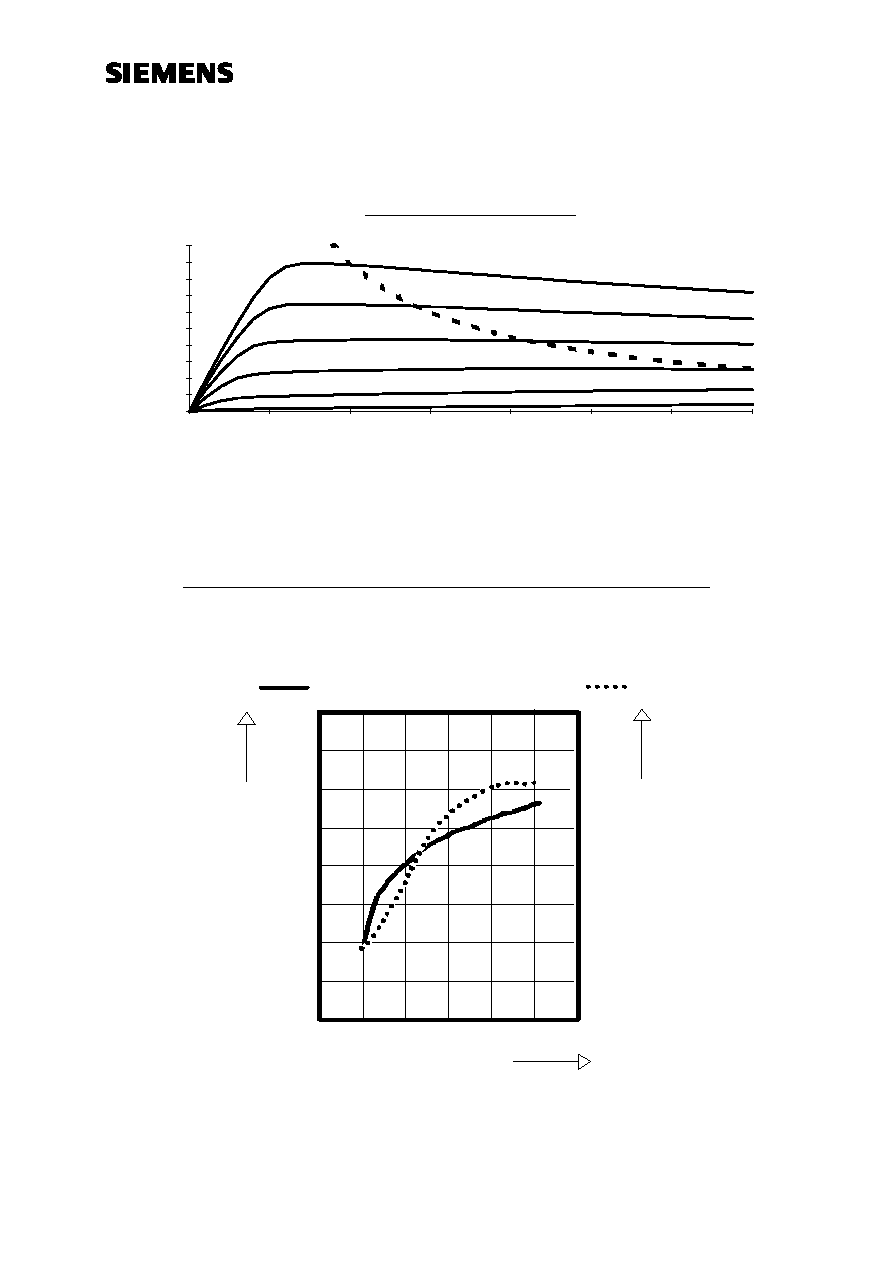
Output Characteristics
Drain-Source Voltage [V]
Draincurrent [A]
0
0,05
0,1
0,15
0,2
0,25
0,3
0,35
0,4
0,45
0,5
0
1
2
3
4
5
6
7
VGS=0V
VGS=-0.5V
VGS=-1V
VGS=-1.5V
VGS=-2V
VGS=-2.5V
PtotDC
Compression Power vs. Drain-Source Voltage
f = 1.8GHz; ID = 0.5IDSS
P1dB
0
5
10
15
20
25
30
35
40
[dBm]
0
1
2
3
4
5
6
[V]
Dra in-Source Voltage
D
0
10
20
30
40
50
60
70
80
[%]

GaAs FET
CLY 2
________________________________________________________________________________________________________
Siemens Aktiengesellschaft
pg. 4/77
17.12.96
HL EH PD 21
typ. Common Source S-Parameters
VDS = 3 V ID = 180 mA
Zo = 50
f GHZ
S11
S21
S12
S22
MAG ANG MAG ANG MAG ANG MAG ANG
0.100
0.99
-12.0
9.17
171.6
0.007
83.3
0.15
-16.6
0.150
0.99
-17.9
9.11
167.4
0.011
80.8
0.16
-24.2
0.200
0.98
-23.7
9.01
163.4
0.014
77.6
0.16
-31.2
0.250
0.97
-29.5
8.89
159.3
0.017
74.7
0.16
-39.0
0.300
0.96
-35.1
8.75
155.4
0.021
72.4
0.16
-45.9
0.400
0.94
-46.0
8.40
147.8
0.026
67.0
0.17
-58.2
0.500
0.92
-56.4
8.03
140.7
0.031
62.5
0.18
-69.2
0.600
0.89
-66.2
7.61
134.1
0.036
58.0
0.18
-79.0
0.700
0.86
-75.4
7.22
128.0
0.039
54.4
0.19
-87.0
0.800
0.84
-84.1
6.82
122.3
0.043
51.2
0.20
-94.2
0.900
0.82
-92.1
6.45
117.2
0.045
48.3
0.20
-100.4
1.000
0.80
-99.7
6.10
112.3
0.048
46.1
0.21
-105.3
1.200
0.77
-113.6
5.45
103.6
0.052
41.8
0.22
-115.1
1.400
0.74
-125.9
4.92
95.8
0.055
38.6
0.23
-122.9
1.500
0.73
-131.5
4.71
92.1
0.056
37.2
0.23
-125.7
1.600
0.72
-137.1
4.48
88.5
0.057
36.2
0.24
-129.4
1.800
0.72
-147.4
4.10
81.7
0.059
34.0
0.25
-135.0
2.000
0.71
-157.2
3.77
75.0
0.060
31.9
0.26
-139.7
2.200
0.71
-165.3
3.47
68.8
0.062
31.2
0.27
-143.0
2.400
0.71
-173.3
3.19
63.0
0.063
29.7
0.29
-147.2
2.500
0.71
-177.4
3.06
60.1
0.063
28.9
0.29
-150.0
3.000
0.72
165.7
2.52
47.2
0.065
28.4
0.32
-159.7
3.500
0.74
151.7
2.12
36.4
0.066
29.7
0.36
-167.5
4.000
0.76
139.9
1.85
26.5
0.073
30.6
0.39
-173.1
4.500
0.78
127.4
1.61
15.3
0.078
28.2
0.42
179.2
5.000
0.79
116.7
1.43
4.6
0.085
24.0
0.45
174.3
5.500
0.80
106.3
1.23
-5.9
0.085
20.9
0.49
167.8
6.000
0.83
97.1
1.06
-14.8
0.087
17.7
0.52
160.9
Additional S-Parameter available on CD

GaAs FET
CLY 2
________________________________________________________________________________________________________
Siemens Aktiengesellschaft
pg. 5/77
17.12.96
HL EH PD 21
typ. Common Source S-Parameters
VDS = 5 V
ID = 180 mA
Zo = 50
f GHZ
S11
S21
S12
S22
MAG ANG MAG ANG MAG ANG MAG ANG
0.100
0.99
-12.3
9.30
171.3
0.007
83.1
0.27
-10.8
0.150
0.99
-18.4
9.23
166.9
0.010
80.0
0.27
-15.8
0.200
0.98
-24.3
9.13
162.8
0.014
77.2
0.26
-20.4
0.250
0.97
-30.3
9.00
158.5
0.017
73.6
0.26
-25.7
0.300
0.96
-36.1
8.85
154.6
0.020
71.1
0.26
-30.5
0.400
0.94
-47.2
8.48
146.7
0.026
65.8
0.26
-39.2
0.500
0.91
-57.8
8.08
139.4
0.030
61.0
0.25
-47.7
0.600
0.89
-67.8
7.64
132.6
0.034
56.3
0.25
-55.4
0.700
0.86
-77.1
7.23
126.3
0.038
52.8
0.25
-62.2
0.800
0.84
-85.9
6.81
120.6
0.041
49.5
0.24
-68.6
0.900
0.81
-93.9
6.43
115.3
0.043
46.4
0.24
-74.1
1.000
0.80
-101.5
6.07
110.4
0.045
44.2
0.24
-79.2
1.200
0.76
-115.4
5.40
101.4
0.048
40.1
0.24
-88.8
1.400
0.74
-127.6 4.87
93.6
0.051
36.9
0.24
-96.8
1.500
0.73
-133.2
4.65
89.8
0.052
35.6
0.24
-100.2
1.600
0.72
-138.8
4.42
86.1
0.052
34.6
0.24
-103.9
1.800
0.72
-149.0
4.04
79.2
0.054
32.7
0.25
-110.4
2.000
0.71
-158.6
3.71
72.3
0.054
30.9
0.26
-116.2
2.200
0.71
-166.6
3.41
66.1
0.055
30.9
0.27
-120.4
2.400
0.71
-174.5
3.13
60.1
0.056
29.9
0.28
-125.6
2.500
0.71
-178.5
3.00
57.1
0.056
29.4
0.29
-129.1
3.000
0.73
164.9
2.47
43.9
0.057
30.8
0.32
-140.6
3.500
0.75
151.1
2.07
32.5
0.059
34.3
0.35
-150.6
4.000
0.77
139.4
1.80
22.1
0.067
36.7
0.40
-158.2
4.500
0.78
126.9
1.56
10.5
0.074
34.7
0.43
-167.6
5.000
0.79
116.1
1.37
-0.6
0.082
30.2
0.47
-174
5.500
0.81
105.6
1.18
-11.6
0.083
26.7
0.51
178
6.000
0.84
96.3
1.00
-20.8
0.086
22.9
0.54
169.6
Additional S-Parameter available on CD
GaAs FET
CLY 2
________________________________________________________________________________________________________
Siemens Aktiengesellschaft
pg. 6/77
17.12.96
HL EH PD 21
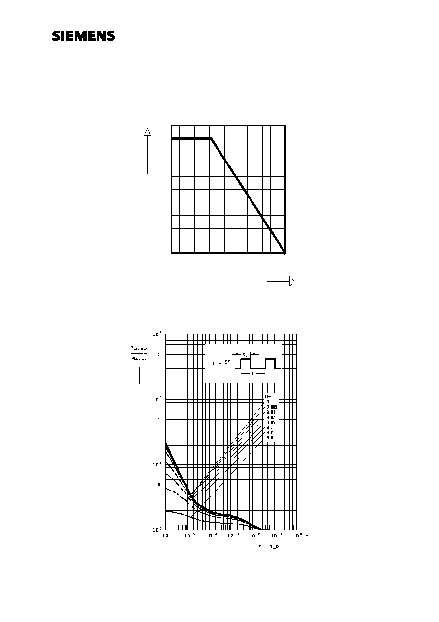
Total Power Dissipation
Ptot = f(Ts)
0
0.2
0.4
0.6
0.8
1.0
[W]
0
50
100
150
Ts
C
O
Permissible Pulse Load
Ptotmax/PtotDC = f(tp)
GaAs FET
CLY 2
________________________________________________________________________________________________________
Siemens Aktiengesellschaft
pg. 7/77
17.12.96
HL EH PD 21
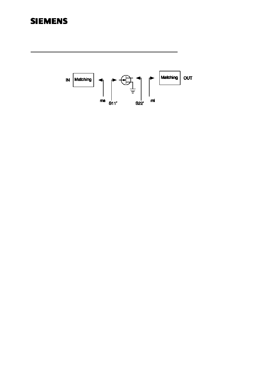
CLY2 Power GaAs-FET Matching Conditions
Definition:
Measured Data:
Typ
f
[GHz]
VDS
[V]
ID
[mA]
P-1dB
[dBm]
Gain
[dB]
ms
MAG
ms
ANG
ml
MAG
ml
ANG
CLY2
0.9
3
175
22.8
15.7
0.49
75
0.42
-165
5
175
25.8
16.5
0.52
75
0.22
-172
6
175
26.9
16.9
0.50
76
0.21
-156
1.5
5
175
25.8
16.1
0.68
106
0.42
143
6
175
26.9
16.9
0.76
113
0.34
139
1.8
2
175
19.0
15.0
0.75
130
0.52
-171
3
175
22.8
15.4
0.70
125
0.45
-172
4
175
24.5
15.6
0.75
131
0.41
166
5
175
25.8
15.7
0.72
131
0.38
163
6
175
26.8
16.0
0.72
135
0.35
155
2.4
3
175
21.5
13.0
0.70
158
0.46
-179
5
175
26.1
13.0
0.67
152
0.36
-178
Note: Gain is small signal gain @
ms and
ml