
BPX 61
Semiconductor Group
357
Silizium-PIN-Fotodiode
Silicon PIN Photodiode
Wesentliche Merkmale
q
Speziell geeignet f¸r Anwendungen im
Bereich von 400 nm bis 1100 nm
q
Kurze Schaltzeit (typ. 20 ns)
q
Hermetisch dichte Metallbauform
(‰hnlich TO-5)
Anwendungen
q
Lichtschranken f¸r Gleich- und
Wechsellichtbetrieb
q
IR-Fernsteuerungen
q
Industrieelektronik
q
"Messen/Steuern/Regeln"
Features
q
Especially suitable for applications from
400 nm to 1100 nm
q
Short switching time (typ. 20 ns)
q
Hermetically sealed metal package
(similar to TO-5)
Application
q
Photointerrupters
q
IR-remote controls
q
Industrial electronics
q
For control and drive circuits
Typ
Type
Bestellnummer
Ordering Code
BPX 61
Q62702-P25
BPX 61
Maþe in mm, wenn nicht anders angegeben/Dimensions in mm, unless otherwise specified.
fmo06011
10.95

BPX 61
Semiconductor Group
358
Grenzwerte
Maximum Ratings
Bezeichnung
Description
Symbol
Symbol
Wert
Value
Einheit
Unit
Betriebs- und Lagertemperatur
Operating and storage temperature range
T
op
;
T
stg
≠ 40 ... + 125
∞
C
Lˆttemperatur (Lˆtstelle 2 mm vom
Geh‰use entfernt bei Lˆtzeit
t
3 s)
Soldering temperature in 2 mm distance
from case bottom (
t
3 s)
T
S
230
∞
C
Sperrspannung
Reverse voltage
V
R
32
V
Verlustleistung,
T
A
= 25
∞
C
Total power dissipation
P
tot
250
mW
Kennwerte (
T
A
= 25
∞
C, Normlicht A,
T
= 2856 K)
Characteristics (
T
A
= 25
∞
C, standard light A,
T
= 2856 K)
Bezeichnung
Description
Symbol
Symbol
Wert
Value
Einheit
Unit
Fotoempfindlichkeit,
V
R
= 5 V
Spectral sensitivity
S
70 (
50)
nA/Ix
Wellenl‰nge der max. Fotoempfindlichkeit
Wavelength of max. sensitivity
S max
850
nm
Spektraler Bereich der Fotoempfindlichkeit
S
= 10 % von
S
max
Spectral range of sensitivity
S
= 10 % of
S
max
400 ... 1100
nm
Bestrahlungsempfindliche Fl‰che
Radiant sensitive area
A
7.00
mm
2
Abmessung der bestrahlungsempfindlichen
Fl‰che
Dimensions of radiant sensitive area
L
◊
B
L
◊
W
2.65
◊
2.65
mm
Abstand Chipoberfl‰che zu Geh‰useober-
fl‰che
Distance chip front to case surface
H
1.9 ... 2.3
mm
Halbwinkel
Half angle
±
55
Grad
deg.
Dunkelstrom,
V
R
= 10 V
Dark current
I
R
2 (
30)
nA

BPX 61
Semiconductor Group
359
Spektrale Fotoempfindlichkeit,
= 850 nm
Spectral sensitivity
S
0.62
A/W
Quantenausbeute,
= 850 nm
Quantum yield
0.90
Electrons
Photon
Leerlaufspannung,
E
v
= 1000 Ix
Open-circuit voltage
V
O
375 (
320)
mV
Kurzschluþstrom,
E
v
= 1000 Ix
Short-circuit current
I
SC
70
µ
A
Anstiegs- und Abfallzeit des Fotostromes
Rise and fall time of the photocurrent
R
L
= 50
;
V
R
= 5 V;
= 850 nm;
I
p
= 800
µ
A
t
r
,
t
f
20
ns
Durchlaþspannung,
I
F
= 100 mA,
E
= 0
Forward voltage
V
F
1.3
V
Kapazit‰t,
V
R
= 0 V,
f
= 1 MHz,
E
= 0
Capacitance
C
0
72
pF
Temperaturkoeffizient von
V
O
Temperature coefficient of
V
O
TC
V
≠ 2.6
mV/K
Temperaturkoeffizient von
I
SC
Temperature coefficient of
I
SC
TC
I
0.18
%/K
Rausch‰quivalente Strahlungsleistung
Noise equivalent power
V
R
= 10 V,
= 850 nm
NEP
4.1
◊
10
≠14
W
Hz
Nachweisgrenze,
V
R
= 10 V,
= 850 nm
Detection limit
D*
6.6
◊
10
12
cm ∑
Hz
W
Kennwerte (
T
A
= 25
∞
C, Normlicht A,
T
= 2856 K)
Characteristics (
T
A
= 25
∞
C, standard light A,
T
= 2856 K)
Bezeichnung
Description
Symbol
Symbol
Wert
Value
Einheit
Unit
BPX 61
Semiconductor Group
360
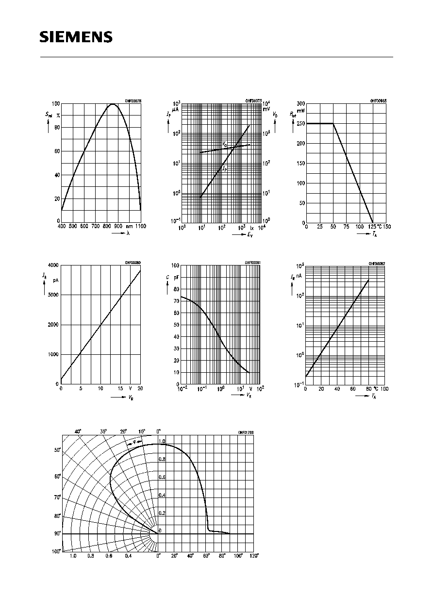
Relative spectral sensitivity
S
rel
=
f
(
)
Dark current
I
R
=
f
(
V
R
),
E
= 0
Photocurrent
I
P
=
f
(
E
v
),
V
R
= 5 V
Open-circuit-voltage
V
O
=
f
(
E
v
)
Capacitance
C
=
f
(
V
R
),
f
= 1 MHz,
E
= 0
Total power dissipation
P
tot
=
f
(
T
A
)
Dark current
I
R
=
f
(
T
A
),
V
R
= 5 V,
E
= 0
Directional characteristics
S
rel
=
f
(
)