Semiconductor Group
2
18/02/1997
BSS 284
Maximum Ratings
Parameter
Symbol
Values
Unit
Chip or operating temperature
T
j
-55 ... + 150
∞C
Storage temperature
T
stg
-55 ... + 150
Thermal resistance, chip to ambient air
1)
R
thJA
350
K/W
Therminal resistance, chip-substrate- reverse side
1)
R
thJSR
285
DIN humidity category, DIN 40 040
E
IEC climatic category, DIN IEC 68-1
55 / 150 / 56
1) For package mounted on aluminium 15 mm x 16.7 mm x 0.7 mm
Electrical Characteristics, at
T
j
= 25∞C, unless otherwise specified
Parameter
Symbol
Values
Unit
min.
typ.
max.
Static Characteristics
Drain- source breakdown voltage
V
GS
= 0 V,
I
D
= -0.25 mA,
T
j
= 25 ∞C
V
(BR)DSS
-50
-
-
V
Gate threshold voltage
V
GS=
V
DS,
I
D
= -1 mA
V
GS(th)
-0.8
-1.2
-1.6
Zero gate voltage drain current
V
DS
= -50 V,
V
GS
= 0 V,
T
j
= 25 ∞C
V
DS
= -50 V,
V
GS
= 0 V,
T
j
= 125 ∞C
V
DS
= -25 V,
V
GS
= 0 V,
T
j
= 25 ∞C
I
DSS
-
-
-
-
-2
-0.1
-0.1
-60
-1
µA
Gate-source leakage current
V
GS
= -20 V,
V
DS
= 0 V
I
GSS
-
-1
-10
nA
Drain-Source on-state resistance
V
GS
= -10 V,
I
D
= -0.13 A
R
DS(on)
-
5
10
Semiconductor Group
3
18/02/1997
BSS 284
Electrical Characteristics, at
T
j
= 25∞C, unless otherwise specified
Parameter
Symbol
Values
Unit
min.
typ.
max.
Dynamic Characteristics
Transconductance
V
DS
2
*
I
D *
R
DS(on)max,
I
D
= -0.13 A
g
fs
0.05
0.08
-
S
Input capacitance
V
GS
= 0 V,
V
DS
= -25 V,
f = 1 MHz
C
iss
-
30
40
pF
Output capacitance
V
GS
= 0 V,
V
DS
= -25 V,
f = 1 MHz
C
oss
-
17
25
Reverse transfer capacitance
V
GS
= 0 V,
V
DS
= -25 V,
f = 1 MHz
C
rss
-
8
12
Turn-on delay time
V
DD
= -30 V,
V
GS
= -10 V,
I
D
= -0.27 A
R
GS
= 50
t
d(on)
-
7
10
ns
Rise time
V
DD
= -30 V,
V
GS
= -10 V,
I
D
= -0.27 A
R
GS
= 50
t
r
-
12
18
Turn-off delay time
V
DD
= -30 V,
V
GS
= -10 V,
I
D
= -0.27 A
R
GS
= 50
t
d(off)
-
10
13
Fall time
V
DD
= -30 V,
V
GS
= -10 V,
I
D
= -0.27 A
R
GS
= 50
t
f
-
20
27
Semiconductor Group
4
18/02/1997
BSS 284
Electrical Characteristics, at
T
j
= 25∞C, unless otherwise specified
Parameter
Symbol
Values
Unit
min.
typ.
max.
Reverse Diode
Inverse diode continuous forward current
T
A
= 25 ∞C
I
S
-
-
-0.13
A
Inverse diode direct current,pulsed
T
A
= 25 ∞C
I
SM
-
-
-0.52
Inverse diode forward voltage
V
GS
= 0 V,
I
F
= -0.26 A,
T
j
= 25 ∞C
V
SD
-
-0.9
-1.2
V
Semiconductor Group
6
18/02/1997
BSS 284
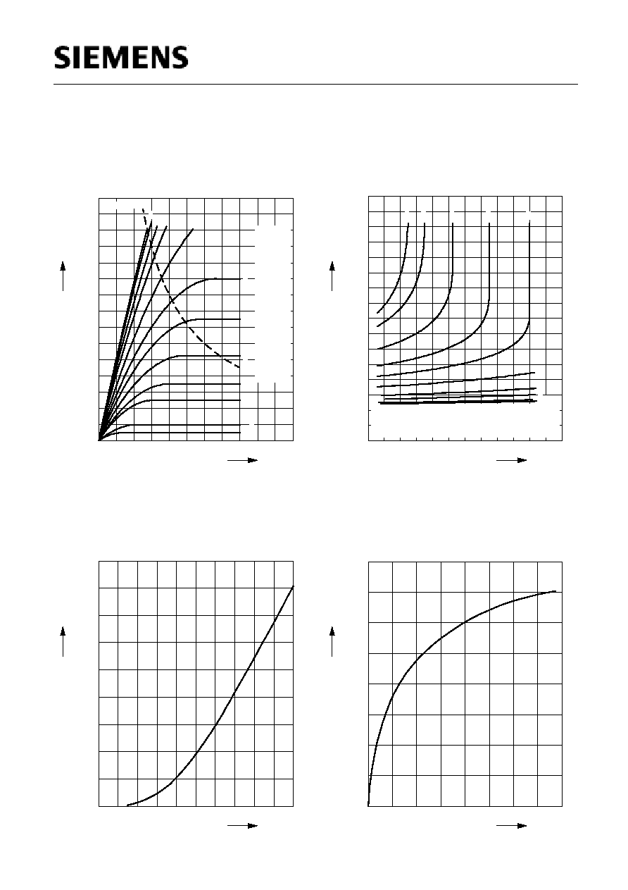
Typ. output characteristics
I
D
=
(
V
DS
)
parameter:
t
p
= 80 µs ,
T
j
= 25 ∞C
0.0
-1.0
-2.0
-3.0
-4.0
V
-5.5
V
DS
0.00
-0.02
-0.04
-0.06
-0.08
-0.10
-0.12
-0.14
-0.16
-0.18
-0.20
-0.22
-0.24
-0.26
A
-0.30
I
D
V
GS
[V]
a
a
-2.0
b
b
-2.5
c
c
-3.0
d
d
-3.5
e
e
-4.0
f
f
-4.5
g
g
-5.0
h
h
-6.0
i
i
-7.0
j
j
-8.0
k
k
-9.0
l
P
tot
= 0W
l
-10.0
Typ. drain-source on-resistance
R
DS (on)
=
(
I
D
)
parameter:
t
p
= 80 µs,
T
j
= 25 ∞C
0.00
-0.04
-0.08
-0.12
-0.16
A
-0.24
I
D
0
4
8
12
16
20
24
32
R
DS (on)
V
GS
[V] =
a
-2.0
V
GS
[V] =
a
-2.5
V
GS
[V] =
a
a
-3.0
b
b
-3.5
c
c
-4.0
d
d
-4.5
e
e
-5.0
f
f
-6.0
g
g
-7.0
h
h
-8.0
i
i
-9.0
j
j
-10.0
Typ. transfer characteristics
I
D
= f(V
GS
)
parameter:
t
p
= 80 µs
V
DS
2 x
I
D
x
R
DS(on)max
0
-1
-2
-3
-4
-5
-6
-7
-8
V
-10
V
GS
0.0
-0.1
-0.2
-0.3
-0.4
-0.5
-0.6
-0.7
A
-0.9
I
D
Typ. forward transconductance
g
fs
=
f (I
D
)
parameter:
t
p
= 80 µs,
V
DS
2 x
I
D
x
R
DS(on)max
0.0
-0.1
-0.2
-0.3
-0.4
-0.5
-0.6
A
-0.8
I
D
0.00
0.02
0.04
0.06
0.08
0.10
0.12
S
0.16
g
fs