Semiconductor Group
1
10.94
q
V
DS
250 V
q
I
D
0.04 A
q
R
DS(on)
100
q
N channel
q
Depletion mode
q
High dynamic resistance
q
Available grouped in
V
GS(th)
Type
Ordering
Code
Tape and Reel
Information
Pin Configuration Marking
Package
1
2
3
BSS 139 Q62702-S612 E6327: 3000 pcs/reel;
G
S
D
STs
SOT-23
BSS 139 Q67000-S221 E7941: 3000 pcs/reel;
V
GS(th)
selected in groups:
(see page 491)
Maximum Ratings
Parameter
Symbol
Values
Unit
Drain-source voltage
V
DS
250
V
Drain-gate voltage,
R
GS
= 20 k
V
DGR
250
Gate-source voltage
V
GS
±
14
Gate-source peak voltage, aperiodic
V
gs
±
20
Continuous drain current,
T
A
= 25 ∞C
I
D
0.04
A
Pulsed drain current,
T
A
= 25 ∞C
I
D puls
0.12
Max. power dissipation,
T
A
= 25 ∞C
P
tot
0.36
W
Operating and storage temperature range
T
j
,
T
stg
≠ 55 ... + 150
∞C
Thermal resistance, chip-ambient
(without heat sink)
chip-substrate ≠ reverse side
1)
R
thJA
R
thJSR
350
285
K/W
DIN humidity category, DIN 40 040
≠
E
≠
IEC climatic category, DIN IEC 68-1
≠
55/150/56
1)
For package mounted on aluminum 15 mm x 16.7 mm x 0.7 mm.
SIPMOS
Æ
Small-Signal Transistor
BSS 139
Semiconductor Group
2
Electrical Characteristics
at
T
j
= 25 ∞C, unless otherwise specified.
Parameter
Symbol
Values
Unit
min.
typ.
max.
Static Characteristics
Drain-source breakdown voltage
V
GS
=
-
3 V,
I
D
= 0.25 mA
V
(BR)DSS
250
≠
≠
V
Gate threshold voltage
V
DS
= 3 V,
I
D
= 1 mA
V
GS(th)
-
1.8
-
1.4
-
0.7
Drain-source cutoff current
V
DS
= 250 V,
V
GS
=
-
3 V
T
j
= 25 ∞C
T
j
= 125 ∞C
I
DSS
≠
≠
≠
≠
100
200
nA
µ
A
Gate-source leakage current
V
GS
= 20 V,
V
DS
= 0
I
GSS
≠
10
100
nA
Drain-source on-resistance
V
GS
= 0 V,
I
D
= 0.014 A
R
DS(on)
≠
75
100
Dynamic Characteristics
Forward transconductance
V
DS
2
◊
I
D
◊
R
DS(on)max
,
I
D
= 0.04 A
g
fs
0.05
0.07
≠
S
Input capacitance
V
GS
= 0,
V
DS
= 25 V,
f
= 1 MHz
C
i
iss
≠
85
120
pF
Output capacitance
V
GS
= 0,
V
DS
= 25 V,
f
= 1 MHz
C
oss
≠
6
10
Reverse transfer capacitance
V
GS
= 0,
V
DS
= 25 V,
f
= 1 MHz
C
rss
≠
2
3
Turn-on time
t
on
, (
t
on
=
t
d(on)
+
t
r
)
V
DD
= 30 V,
V
GS
=
-
2 V ... + 5 V,
R
GS
= 50
,
I
D
= 0.15 A
t
d(on)
≠
4
6
ns
t
r
≠
10
15
Turn-off time
t
off
, (
t
off
=
t
d(off)
+
t
f
)
V
DD
= 30 V,
V
GS
=
-
2 V ... + 5 V,
R
GS
= 50
,
I
D
= 0.15 A
t
d(off)
≠
10
13
t
f
≠
15
20
BSS 139
Semiconductor Group
3
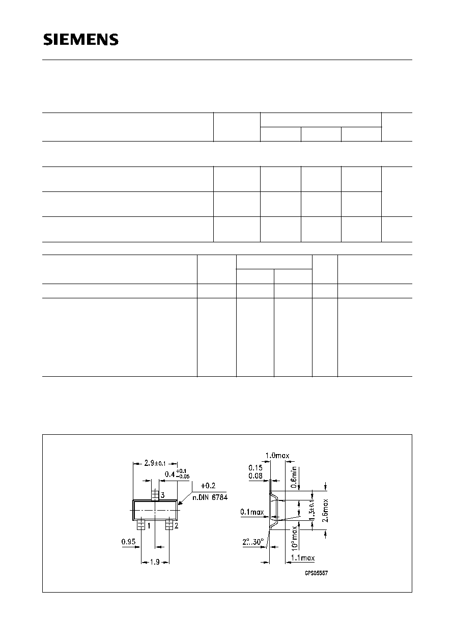
Package Outline
1) A specific group cannot be ordered separately.
Each reel only contains transistors from one group.
Electrical Characteristics (cont'd)
at
T
j
= 25 ∞C, unless otherwise specified.
Parameter
Symbol
Values
Unit
min.
typ.
max.
Reverse Diode
Continuous reverse drain current
T
A
= 25 ∞C
I
S
≠
≠
0.04
A
Pulsed reverse drain current
T
A
= 25 ∞C
I
SM
≠
≠
0.12
Diode forward on-voltage
I
F
= 0.08 A,
V
GS
= 0
V
SD
≠
0.7
1.2
V
V
GS(th)
Grouping
Symbol
Limit Values
Unit
Test Condition
min.
max.
Range of
V
GS(th)
V
GS(th)
≠
0.15
V
≠
Threshold voltage selected in groups:
1)
F
G
A
B
C
D
V
GS(th)
≠ 1.535
≠ 1.635
≠ 1.735
≠ 1.835
≠ 1.935
≠ 2.035
≠ 1.385
≠ 1.485
≠ 1.585
≠ 1.685
≠ 1.785
≠ 1.885
V
V
V
V
V
V
V
DS1
= 0.2 V;
V
DS2
= 3 V;
I
D
= 10
µ
A
SOT-23
Dimensions in mm
BSS 139
Semiconductor Group
4
Characteristics
at
T
j
= 25 ∞C, unless otherwise specified.
Total power dissipation
P
tot
=
f
(
T
A
)
Typ. output characteristics
I
D
=
f
(
V
DS
)
parameter:
t
p
= 80
µ
s
Safe operating area
I
D
=
f
(
V
DS
)
parameter:
D
= 0.01,
T
C
= 25 ∞C
Typ. drain-source on-resistance
R
DS(on)
=
f
(
I
D
)
parameter:
V
GS
BSS 139
Semiconductor Group
5
Typ. transfer characteristics
I
D
=
f
(
V
GS
)
parameter:
t
p
= 80
µ
s,
V
DS
2
◊
I
D
◊
R
DS(on)max.
Drain-source on-resistance
R
DS(on)
=
f
(
T
j
)
parameter:
I
D
= 0.014 A,
V
GS
= 0 V, (spread)
Typ. forward transconductance
g
fs
=
f
(
I
D
)
parameter:
V
DS
2
◊
I
D
◊
R
DS(on)max.
,
t
p
= 80
µ
s
Typ. capacitances
C
=
f
(
V
DS
)
parameter:
V
GS
= 0,
f
= 1 MHz
BSS 139
Semiconductor Group
6
Gate threshold voltage
V
GS(th)
=
f
(
T
j
)
parameter:
V
DS
= 3 V,
I
D
= 1 mA, (spread)
Drain current
I
D
=
f
(
T
A
)
parameter:
V
GS
3 V
Forward characteristics of reverse diode
I
F
=
f
(
V
SD
)
parameter:
t
p
= 80
µ
s,
T
j
,
(spread)
Drain-source breakdown voltage
V
(BR) DSS
=
b
◊
V
(BR)DSS
(25 ∞C)
BSS 139