Semiconductor Group
1
11.96
Features
q
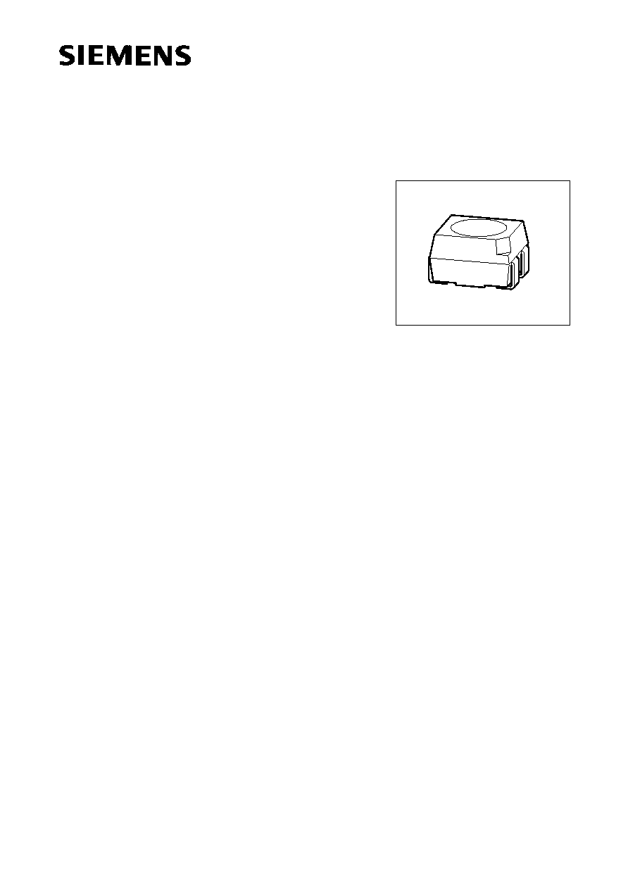
P-LCC-4 package
q
color of package: white
q
for use as optical indicator
q
appropriate for high ambient light because of the higher operation current (
50 mA DC)
q
for backlighting, optical coupling into light pipes and lenses
q
both chips can be controlled separately
q
suitable for all SMT assembly and soldering methods
q
available taped on reel (8 mm tape)
q
load dump resistant acc. to DIN 40839
Super Multi TOPLED
Æ
High-Current LED
LSS T672, LOO T672, LYY T672
LGG T672, LPP T672
Besondere Merkmale
q
Geh‰usebauform: P-LCC-4
q
Geh‰usefarbe: weiþ
q
als optischer Indikator einsetzbar
q
besonders geeignet bei hohem Umgebungslicht durch
erhˆhten Betriebsstrom (
50 mA DC)
q
zur Hinterleuchtung, Lichtleiter- und Linseneinkopplung
q
beide Leuchtdiodenchips getrennt ansteuerbar
q
f¸r alle SMT-Best¸ck- und Lˆttechniken geeignet
q
gegurtet (8-mm-Filmgurt)
q
Stˆrimpulsfest nach DIN 4083
VPL06837

Semiconductor Group
2
LSS T672, LOO T672, LYY T672
LGG T672, LPP T672
s
Not for new design / Nicht f¸r Neuentwicklungen
Streuung der Lichtst‰rke in einer Verpackungseinheit
I
V max
/
I
V min
2.0.
1)
Streuung der Lichtst‰rke in einer LED
I
V max
/
I
V min
2.0.
1)
Bei MULTILED
Æ
mit 2 gleichfarbigen Chips in einem Geh‰use wird die Helligkeitsgruppe aus dem Mittelwert
der Lichtst‰rken ermittelt.
Luminous intensity ratio in one packaging unit
I
V max
/
I
V min
2.0.
1)
Luminous intensity ratio in one LED
I
V max
/
I
V min
2.0.
1)
In case of MULTILED
Æ
with two chips of the same color in one package, the mean of the brightness determines
the brightness group of the LED.
Typ
Type
Emissions-
farbe
Color of
Emission
Farbe der
Lichtaustritts-
fl‰che
Color of the
Light Emitting
Area
Lichtst‰rke
Luminous
Intensity
I
F
= 50 mA
I
V
(mcd)
Lichtstrom
Luminous
Flux
I
F
= 50 mA
V
(mlm)
Bestellnummer
Ordering Code
LSS T672-NO
super-red /
super-red
colorless clear
25
(100 typ.)
300 (typ.)
Q62703-Q2881
LOO T672-MO orange /
orange
colorless clear
16
(100 typ.)
300 (typ.)
Q62703-Q2536
LYY T672-NO
yellow /
yellow
colorless clear
25
(100 typ.)
300 (typ.)
Q62703-Q2883
LGG T672-NO
green /
green
colorless clear
25
(100 typ.)
300 (typ.)
Q62703-Q2884
LPP T672-MO
pure green /
pure green
colorless clear
16
(50 typ.)
150 (typ.)
Q62703-Q2885
s
s
s
Semiconductor Group
3
Grenzwerte
Maximum Ratings
Bezeichnung
Parameter
Symbol
Symbol
Werte
Values
Einheit
Unit
Betriebstemperatur
Operating temperature range
T
op
≠ 55 ... + 100
∞C
Lagertemperatur
Storage temperature range
T
stg
≠ 55 ... + 100
∞C
Sperrschichttemperatur
Junction temperature
T
j
+ 100
∞C
Durchlaþstrom
Forward current
I
F
50
mA
Stoþstrom
Surge current
t
10
µ
s,
D
= 0.005
I
FM
1
A
Sperrspannung
Reverse voltage
V
R
5
V
Verlustleistung
Power dissipation
P
tot
160
mW
W‰rmewiderstand
Thermal resistance
Sperrschicht / Umgebung
Junction / air
Montage auf PC-Board*
)
(Padgrˆþe
16 mm
2
)
mounted on PC board*
)
(pad size
16 mm
2
)
R
th JA
1)
R
th JA
2)
380
530
K/W
K/W
*
)
PC-board: FR4
1)
nur ein Chip betrieben
1)
one system on
2)
beide Chips betrieben
2)
both systems on simultaneously
Notes
Die angegebenen Grenzdaten gelten f¸r einen Chip.
The stated maximum ratings refer to one chip.
LSS T672, LOO T672, LYY T672
LGG T672, LPP T672

Semiconductor Group
4
Kennwerte (
T
A
= 25 ∞C)
Characteristics
Bezeichnung
Parameter
Symbol
Symbol
Werte
Values
Einheit
Unit
LS
LO
LY
LG
LP
Wellenl‰nge des emittierten Lichtes
(typ.)
Wavelength at peak emission
(typ.)
I
F
= 10 mA
peak
635
610
586
565
557
nm
Dominantwellenl‰nge
(typ.)
Dominant wavelength
(typ.)
I
F
= 10 mA
dom
628
605
590
570
560
nm
Spektrale Bandbreite bei 50 %
I
rel max
(typ.)
Spectral bandwidth at 50 %
I
rel max
(typ.)
I
F
= 10 mA
45
40
45
25
22
nm
Abstrahlwinkel bei 50 %
I
v
(Vollwinkel)
Viewing angle at 50 %
I
v
2
120
120
120
120
120
deg.
Durchlaþspannung
(typ.)
Forward voltage
(max.)
I
F
= 50 mA
V
F
V
F
2.0
3.8
2.1
3.8
2.2
3.8
2.6
3.8
2.6
3.8
V
V
Sperrstrom
(typ.)
Reverse current
(max.)
V
R
= 5 V
I
R
I
R
0.01
10
0.01
10
0.01
10
0.01
10
0.01
10
µ
A
µ
A
Kapazit‰t
(typ.)
Capacitance
V
R
= 0 V,
f
= 1 MHz
C
0
40
35
35
60
80
pF
Schaltzeiten:
Switching times:
I
V
from 10 % to 90 %
(typ.)
I
V
from 90 % to 10 %
(typ.)
I
F
= 100 mA,
t
p
= 10
µ
s,
R
L
= 50
t
r
t
f
350
200
500
250
350
200
500
250
500
250
ns
ns
LSS T672, LOO T672, LYY T672
LGG T672, LPP T672

Semiconductor Group
5
LSS T672, LOO T672, LYY T672
LGG T672, LPP T672
Relative spektrale Emission
I
rel
=
f
(
),
T
A
= 25 ∞C,
I
F
= 10 mA
Relative spectral emission
V (
) = spektrale Augenempfindlichkeit
Standard eye response curve
Abstrahlcharakteristik
I
rel
=
f
(
)
Radiation characteristic
Semiconductor Group
6
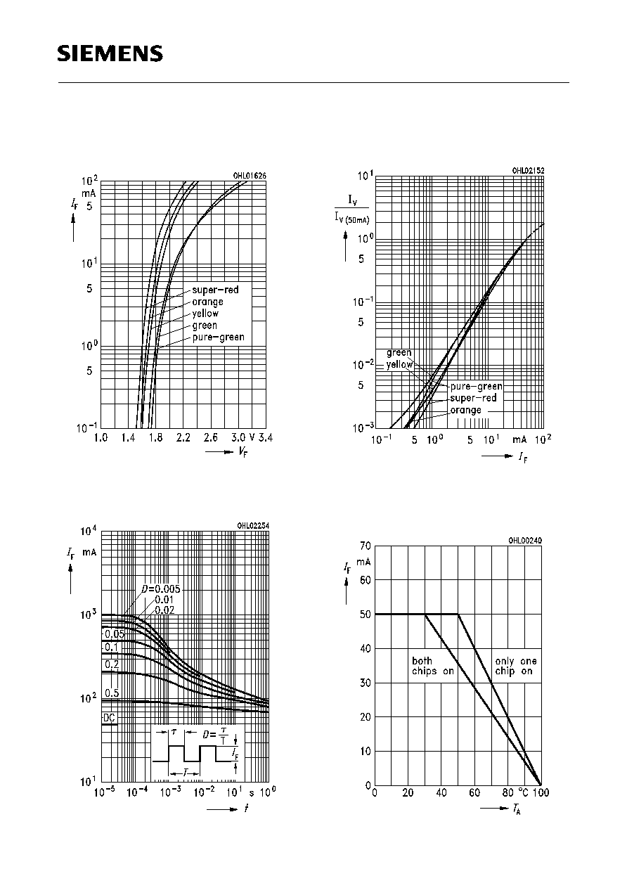
Durchlaþstrom
I
F
=
f
(
V
F
)
Forward current
T
A
= 25 ∞C
Zul‰ssige Impulsbelastbarkeit
I
F
=
f
(
t
p
)
Permissible pulse handling capability
Duty cycle
D
= parameter,
T
A
= 25 ∞C
Relative Lichtst‰rke
I
V
/
I
V(50 mA)
=
f
(
I
F
)
Relative luminous intensity
T
A
= 25 ∞C
Maximal zul‰ssiger Durchlaþstrom
I
F
=
f
(
T
A
)
Max. permissible forward current
LSS T672, LOO T672, LYY T672
LGG T672, LPP T672

Semiconductor Group
7
LSS T672, LOO T672, LYY T672
LGG T672, LPP T672
Wellenl‰nge der Stahlung
peak
=
f (T
A
)
Wavelength at peak emission
I
F
= 10 mA
Durchlaþspannung
V
F
=
f
(
T
A
)
Forward voltage
I
F
= 50 mA
Dominantwellenl‰nge
dom
=
f
(
T
A
)
Dominat wavelength
I
F
= 10 mA
Relative Lichtst‰rke
I
V
/
I
V(25 ∞C)
=
f
(
T
A
)
Relative luminous intensity
I
F
= 50 mA
Semiconductor Group
8
LSS T672, LOO T672, LYY T672
LGG T672, LPP T672
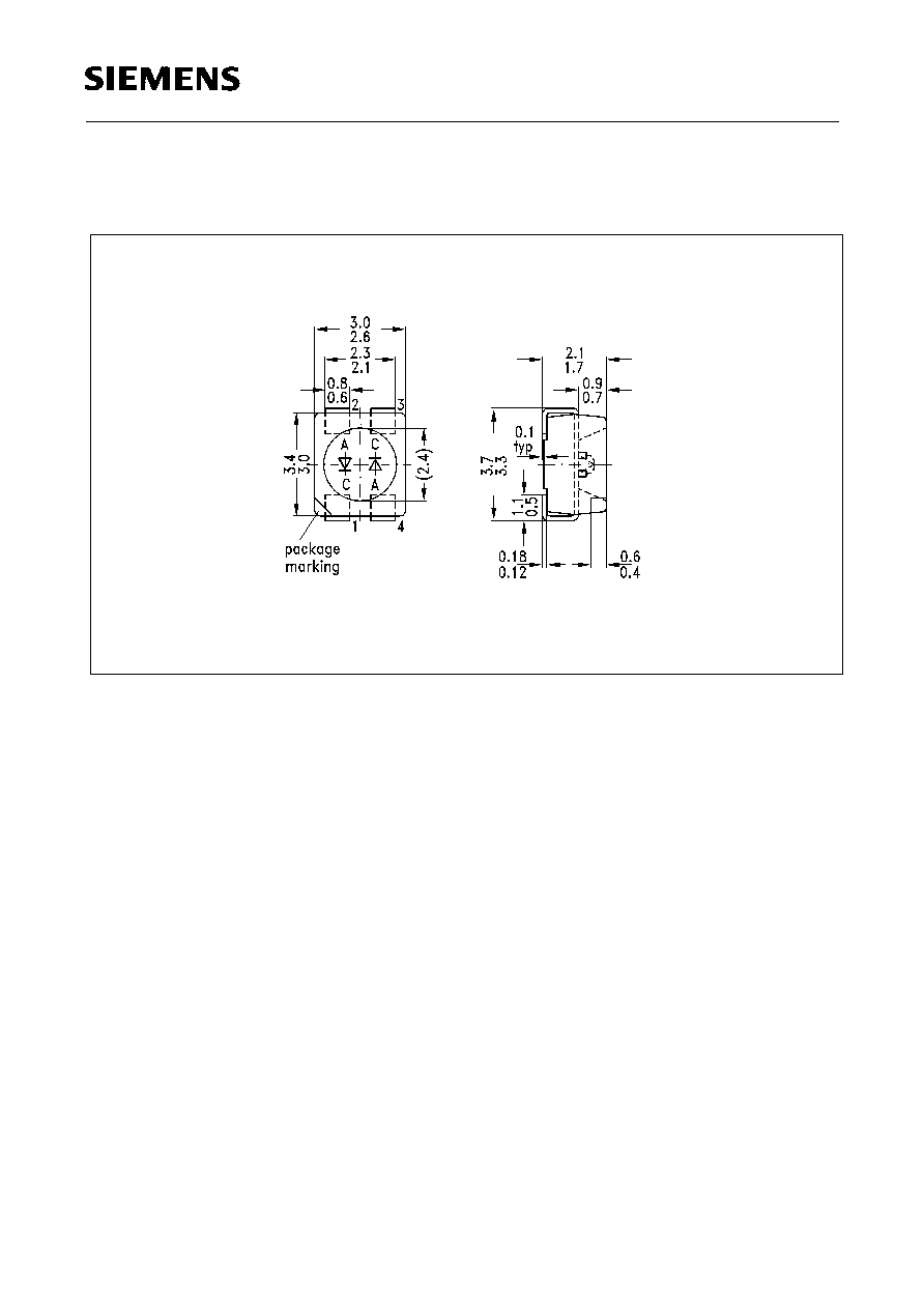
Maþzeichnung
(Maþe in mm, wenn nicht anders angegeben)
Package Outlines
(Dimensions in mm, unless otherwise specified)
GPL06837