Semiconductor Group
1
1998-11-05
VPL06837
Besondere Merkmale
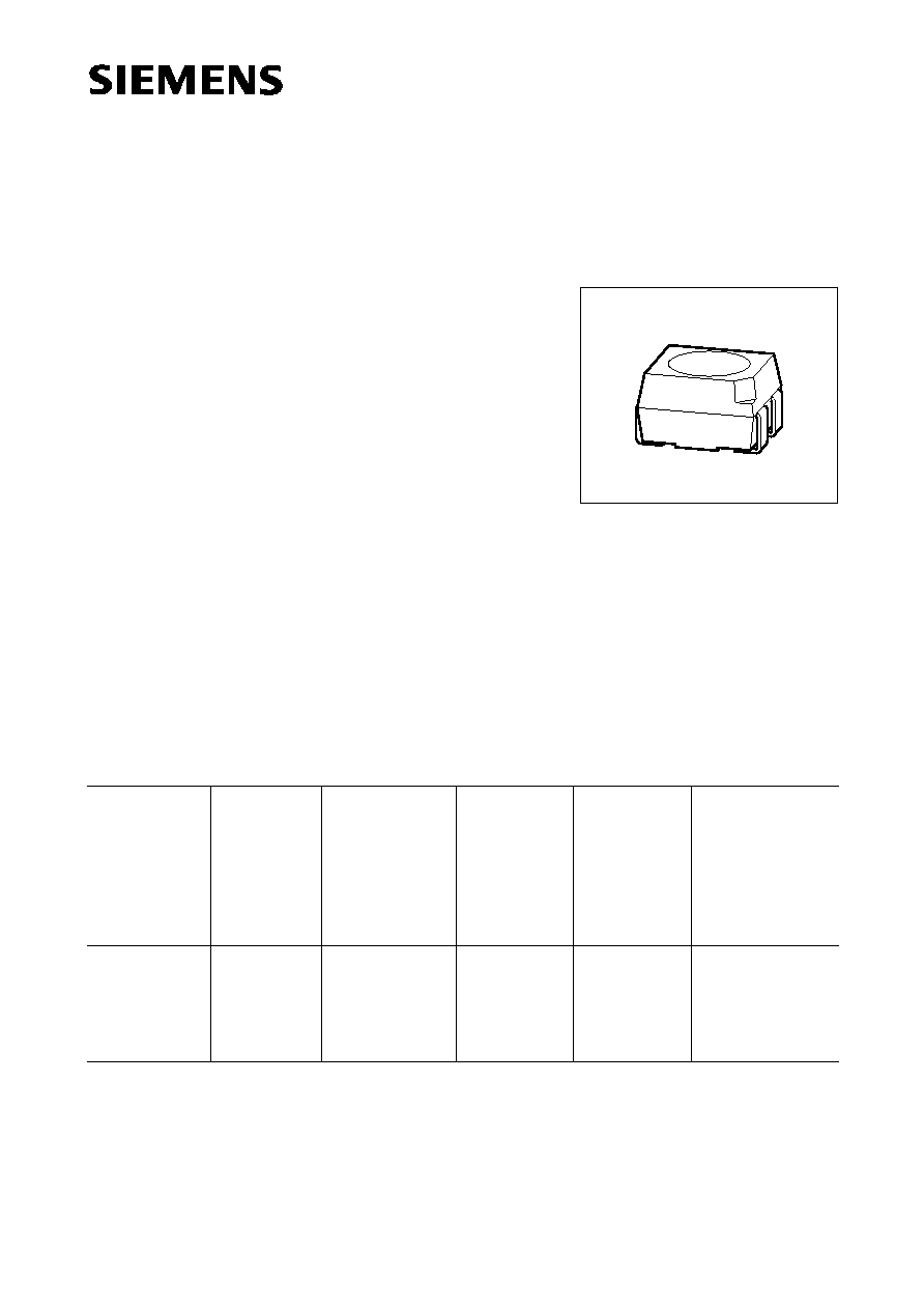
∑ Geh‰usebauform: P-LCC-4
∑ Geh‰usefarbe: weiþ
∑ als optischer Indikator einsetzbar
∑ zur Hintergrundbeleuchtung, Lichtleiter- und
Linseneinkopplung
∑ f¸r alle SMT-Best¸cktechniken geeignet
∑ gegurtet (8 mm-Filmgurt)
∑ JEDEC Level 3
∑ nur IR Reflow Lˆten
Features
∑ P-LCC-4 package
∑ color of package: white
∑ for use as optical indicator
∑ for backlighting, optical coupling into light pipes and lenses
∑ suitable for all SMT assembly methods
∑ available taped on reel (8 mm tape)
∑ JEDEC Level 3
∑ IR reflow soldering only
Power TOPLED
Æ
Hyper-Bright LED
Vorl‰ufige Daten / Preliminary Data
LY E676
Streuung der Lichtst‰rke in einer Verpackungseinheit
I
V max
/
I
V min
1.6.
Luminous intensity ratio in one packaging unit
I
V max
/
I
V min
1.6.
Helligkeitswerte werden bei einer Strompulsdauer von 25 ms spezifiziert.
Luminous intensity is specified at a current pulse duration of 25 ms.
Typ
Type
Emissions-
farbe
Color of
Emission
Farbe der
Lichtaustritts-
fl‰che
Color of the
Light Emitting
Area
Lichtst‰rke
Luminous
Intensity
I
F
= 50 mA
I
V
(mcd)
Lichtstrom
Luminous
Flux
I
F
= 50 mA
V
(mlm)
Bestellnummer
Ordering Code
LY E676
LY E676-T1
LY E676-T2
LY E676-U1
LY E676-U2
yellow
colorless clear
250
... 400
320
... 500
400
... 630
500
... 800
900 (typ.)
1200 (typ.)
1500 (typ.)
1800 (typ.)
Q62703-Q3759

LY E676
Semiconductor Group
2
1998-11-05
Grenzwerte
Maximum Ratings
Bezeichnung
Parameter
Symbol
Symbol
Werte
Values
Einheit
Unit
Betriebstemperatur
Operating temperature range
T
op
≠ 40 ... + 100
∞C
Lagertemperatur
Storage temperature range
T
stg
≠ 40 ... + 100
∞C
Sperrschichttemperatur
Junction temperature
T
j
+ 120
∞C
Durchlaþstrom
Forward current
I
F
50
mA
Sperrspanung
1)
Reverse voltage
1)
V
R
3
V
Verlustleistung
Power dissipation
T
A
25 ∞C
P
tot
130
mW
W‰rmewiderstand
Thermal resistance
Sperrschicht / Umgebung
Junction / air
Montage auf PC-board*
)
(Padgrˆþe
12 mm
2
)
mounted on PC board*
)
(pad size
12 mm
2
)
R
th JA
290
K/W
1)
Belastung in Sperrichtung sollte vermieden werden.
1)
Reverse biasing should be avoided.
*
)
PC-board: FR4
LY E676
Semiconductor Group
3
1998-11-05
Kennwerte (
T
A
= 25 ∞C)
Characteristics
1)
Durchlaþspannungsgruppen
2)
Wellenl‰ngengruppen
Forward voltage groups
Wavelength groups
Bezeichnung
Parameter
Symbol
Symbol
Werte
Values
Einheit
Unit
typ.
max.
Wellenl‰nge des emittierten Lichtes
Wavelength at peak emission
I
F
= 50 mA
peak
594
≠
nm
Dominantwellenl‰nge
2)
Dominant wavelength
2)
I
F
= 50 mA
dom
590
≠
nm
Spektrale Bandbreite bei 50%
I
rel max
Spectral bandwidth at 50%
I
rel max
I
F
= 50 mA
17
≠
nm
Abstrahlwinkel bei 50%
I
v
(Vollwinkel)
Viewing angle at 50%
I
v
2
120
≠
Grad
deg.
Durchlaþspannung
1)
Forward voltage
1)
I
F
= 50 mA
V
F
2.1
2.55
V
Sperrstrom
Reverse current
V
R
= 3 V
I
R
0.01
10
µ
A
Temperaturkoeffizient von
dom
(
I
F
= 50 mA)
Temperature coefficient of
dom
(
I
F
= 50 mA)
TC
t.b.d.
≠
nm/K
Temperaturkoeffizient von
peak
(
I
F
= 50 mA)
Temperature coefficient of
peak
(
I
F
= 50 mA)
TC
t.b.d.
≠
nm/K
Temperaturkoeffizient von
V
F
(
I
F
= 50 mA)
Temperature coefficient of
V
F
(
I
F
= 50 mA)
TC
V
t.b.d.
≠
mV/K
Temperaturkoeffizient von
I
V
(
I
F
= 50 mA)
Temperature coefficient of
I
V
(
I
F
= 50 mA)
TC
I
t.b.d.
≠
%/K
Gruppe
Group
Durchlaþspannung
Forward voltage
Einheit
Unit
Gruppe
Group
Wellenl‰nge
Wavelength
Einheit
Unit
min.
max.
min.
max.
1
1.85
2.25
V
1
585
590
nm
2
2.15
2.55
V
2
588
593
nm
3
591
596
nm
V
LY E676
Semiconductor Group
4
1998-11-05
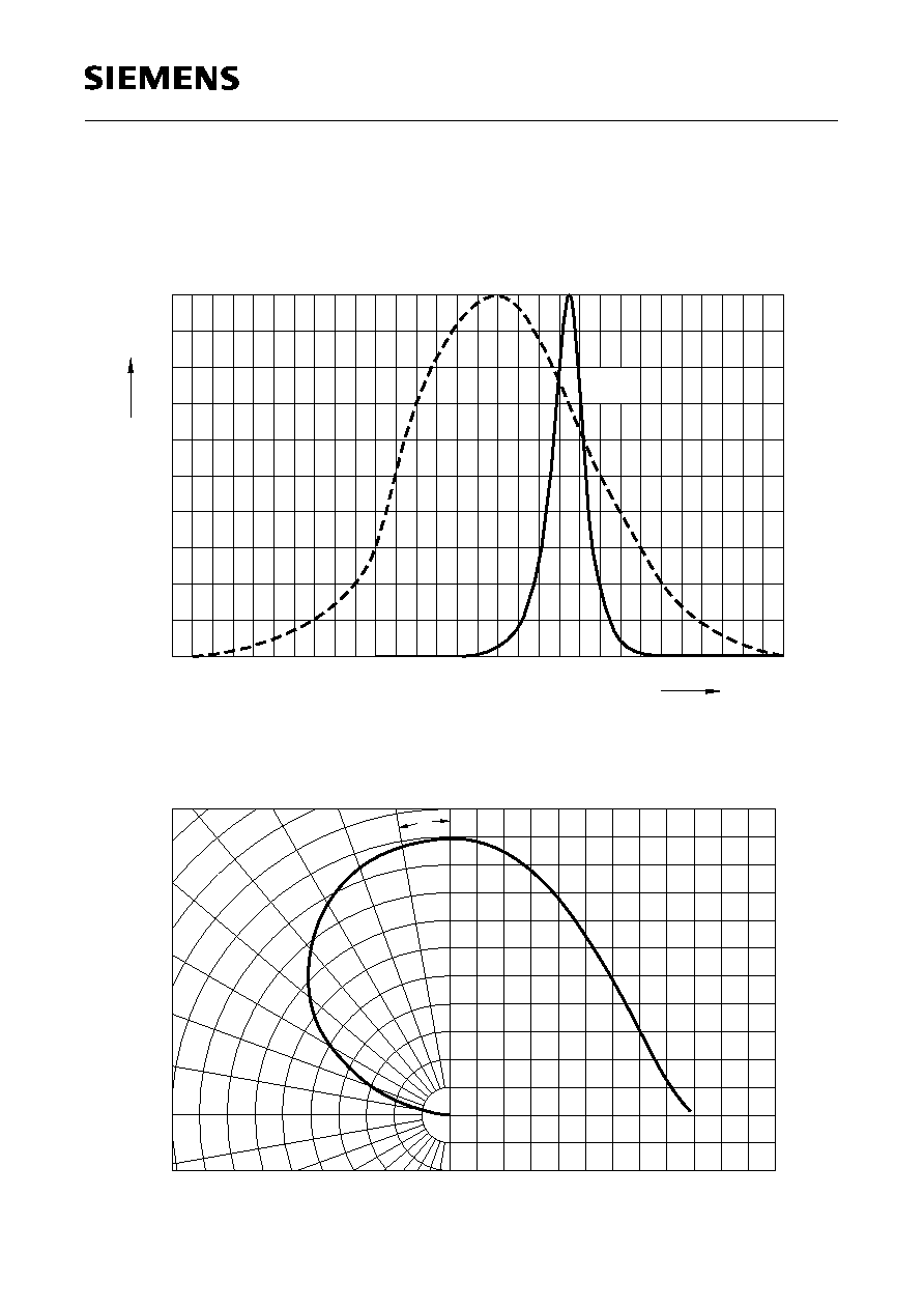
Relative spektrale Emission
I
rel
=
f
(
),
T
A
= 25 ∞C,
I
F
= 50 mA
Relative spectral emission
V(
) =
spektrale Augenempfindlichkeit
Standard eye response curve
Abstrahlcharakteristik
I
rel
=
f
(
)
Radiation characteristic
OHL00443
400
0
20
40
60
80
100
450
500
550
600
650
700
nm
%
rel
V
yellow
0
0.2
0.4
1.0
0.8
0.6
1.0
0.8
0.6
0.4
0∞
10∞
20∞
40∞
30∞
OHL01660
50∞
60∞
70∞
80∞
90∞
100∞
0∞
20∞
40∞
60∞
80∞
100∞
120∞
LY E676
Semiconductor Group
5
1998-11-05
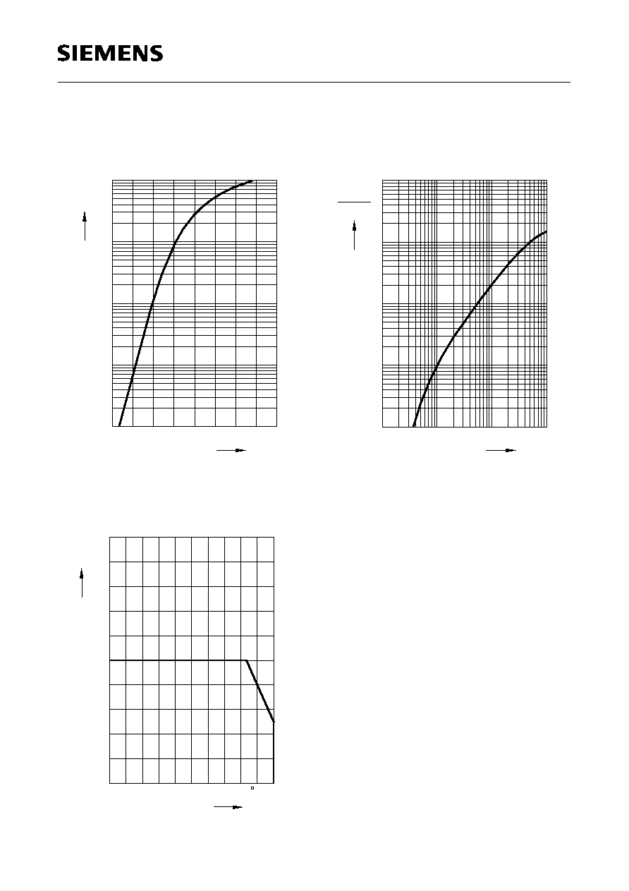
Durchlaþstrom
I
F
=
f
(
V
F
)
Forward current
T
A
= 25 ∞C
Maximal zul‰ssiger Durchlaþstrom
Max. permissible forward current
I
F
=
f
(
T
A
)
Relative Lichtst‰rke
I
V
/
I
V(50 mA)
=
f
(
I
F
)
Relative luminous intensity
T
A
= 25 ∞C
V
OHL00444
F
F
1.6
mA
10
1
10
5
-2
5
0
10
-1
5
10
1.8
2.0
2.2
V
2.4
10
2
T
OHL00446
A
0
F
0
20
40
60
80 C 100
mA
20
40
60
80
100
OHL00445
F
-1
10
V (50 mA)
10
-3
-2
-1
0
1
10
10
10
10
10
0
10
1
10
2
5
5
5
5
5
mA
V
LY E676
Semiconductor Group
6
1998-11-05
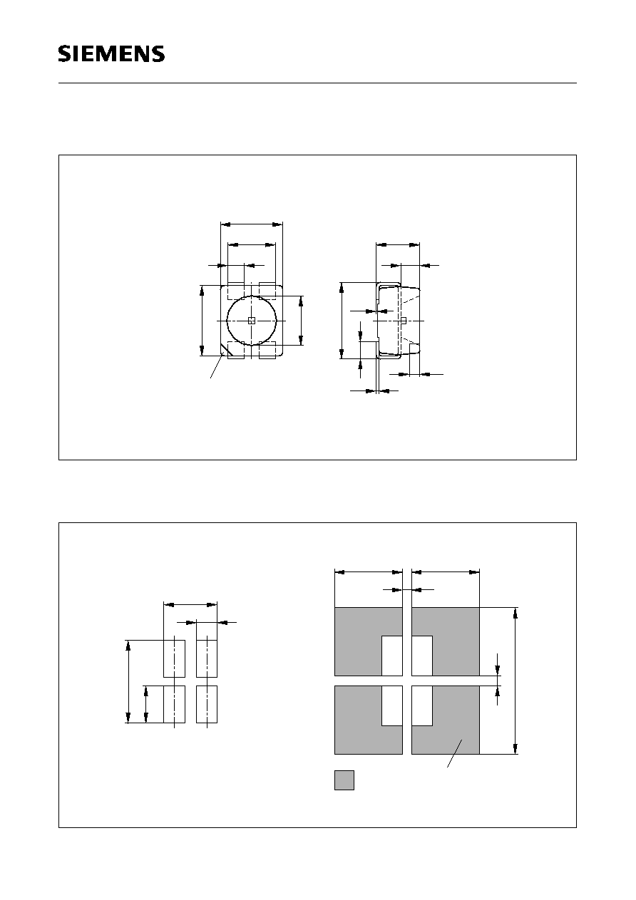
Maþzeichnung
(Maþe in mm, wenn nicht anders angegeben)
Package Outlines
(Dimensions in mm, unless otherwise specified)
Empfehlung Lˆtpaddesign Infrarot/Vapor-Phase Reflow-Lˆtung
Recommended Pad
Infrared Vapor-Phase Reflow-Soldering
(2.4)
3.4
3.0
3.0
2.6
2.1
2.3
0.8
0.6
2.1
1.7
0.9
0.7
3.3
3.7
1.1
0.5
0.1 typ
0.12
0.18
0.6
0.4
C
C
A
C
package
marking
C: Cathode
A: Anode
GPL06991
2.6
1.85
1.1
4.2
Padgeometrie f¸r
verbesserte W‰rmeableitung
improved heat dissipation
Paddesign for
3.3
3.3
0.4
7.5
0.5
Lˆtstoplack
solder resist
= 12 mm per pad
Cu Fl‰che / Cu-area
2
OHLP0439
LY E676
Semiconductor Group
7
1998-11-05
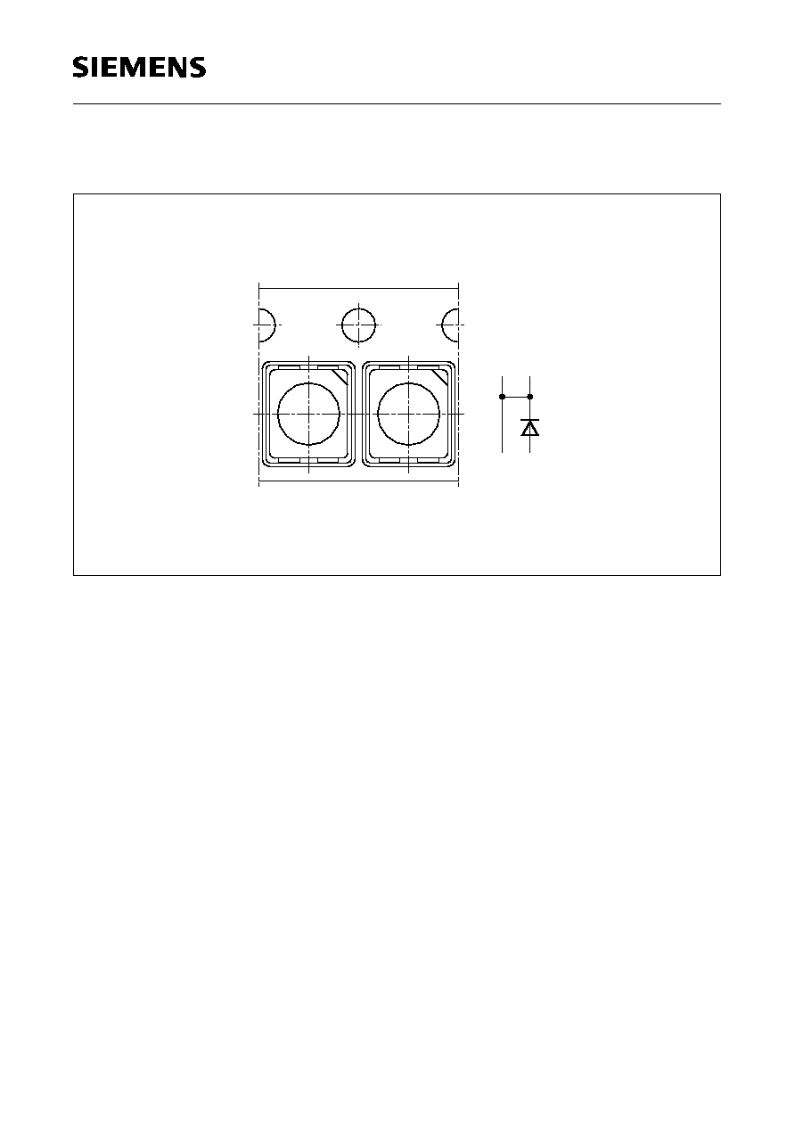
Gurtung
Taping
C
C
A
C
OHA00440