
Semiconductor Group
1
TCA 305
TCA 355
TCA 305
TCA 355
Bipolar IC
Features
q
Lower open-loop current consumption;
I
S
< 1 mA
q
Lower output saturation voltage
q
The temperature dependence of the switching
distance is lower and compensation of the resonant
circuit
TC (temperature coefficient) is easier
q
The sensitivity is higher, so that larger switching
distances are possible and coils of a lower quality can
be used
q
The switching hysteresis remains constant as regards
temperature, supply voltage and switching distance
q
The TCA 305 even functions without external
integrating capacitor. With an external capacitor (or
with RC combination) good noise immunity can be
achieved
q
The outputs are temporarily short-circuit proof (approx.
10 s to 1 min depending on package)
q
The outputs are disabled when
V
S
< approx. 4.5 V and
are enabled when the oscillator stabilizes
(from
V
S min
= 5 V)
q
Higher switching frequencies can be obtained
q
Miniature package
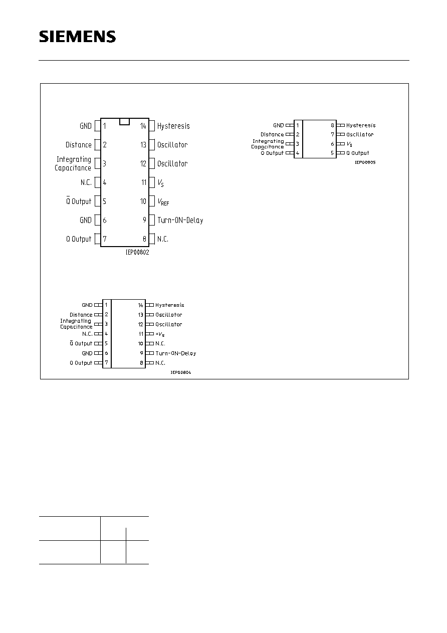
Proximity Switch
P-DSO-8-1
P-DIP-14-1
P-DSO-14-1
Type
Ordering Code
TCA 305 A
Q67000-A2291
Package
P-DIP-14-1
TCA 305 G
Q67000-A2305
P-DSO-14-1 (SMD)
TCA 355 G
Q67000-A2444
P-DSO-8-1 (SMD)
s
s
Not for new design
01.96
Semiconductor Group
2
TCA 305
TCA 355
TCA 305 A
TCA 305 G
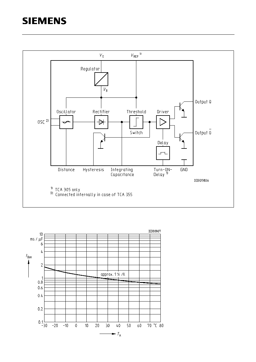
The devices TCA 305 and TCA 355 contain all the functions necessary to design inductive
proximity switches. By approaching a standard metal plate to the coil, the resonant circuit is
damped and the outputs are switched.
Operation Schematic: see TCA 205
The types TCA 305 and TCA 355 have been developed from the type TCA 205 and are out-
standing for the following characteristics:
Logic Functions
Oscillator
Outputs
Q
not damped
damped
H
L
L
H
TCA 355 G
Pin Configurations (top view)
Semiconductor Group
3
TCA 305
TCA 355
Block Diagram
Standard Turn-ON Delay Referred to
T
A
= 25 ∞C
Semiconductor Group
4
TCA 305
TCA 355
Absolute Maximum Ratings
Operating Range
Characteristics
V
S
= 12 V,
T
A
= ≠ 25 to 85 ∞C
Parameter
Symbol
Unit
Limit Values
Supply voltage
Output voltage
V
S
V
Q
35
35
Output current
I
Q
mA
50
V
V
Junction temperature
Storage temperature range
T
j
T
stg
150
≠ 55 to 125
∞C
∞C
Thermal resistance
system - air
TCA 305 A
TCA 305 G
R
th SA
R
th SA
85 (135)
2)
140 (200)
2)
K/W
K/W
Distance, hysteresis resistance
R
Di
,
R
Hy
0
Capacitances
C
I
,
C
D
µ
F
5
Supply voltage
V
S
V
5 to 30
3)
Oscillator frequency
f
OSC
MHz
0.015 to 1.5
Ambient temperature
T
A
∞C
≠ 25 to 85
Parameter
typ.
min.
max.
Unit
Test
Condition
Limit Values
Symbol
Open-loop
current consumption
0.6
0.9
(1.0)
2)
mA
outputs open
I
S
Reference voltage
1)
L-output voltage
per output
3.2
0.04
0.10
0.22
0.15
0.35
0.75
V
V
V
V
I
REF
< 10
µ
A
I
Q L
= 5 mA
I
Q L
= 25 mA
I
Q L
= 50 mA
V
REF
V
Q L
V
Q L
V
Q L
H-output current per output
10
µ
A
V
Q H
= 30 V
I
Q H
Threshold at 3
Hysteresis at 3
2.1
0.5
0.4
0.6
V
V
V
S 3
V
Hy
Turn-ON delay
1)
600
≠ 25 %
≠ 25 %
ms/
µ
F
T
A
= 25 ∞C
t
D ON
Switching frequency w/o
C
I
5
kHz
f
S
1)
TCA 305 only
2)
Values in parenthesis apply to TCA 355 only
3)
Operation at voltages less than 5 V (between approx. 2.5 and 5 V) is possible, if
V
REF
is connected to
V
S
. In
this case
V
REF
is no longer internally stabilized. Additionally, the pin "turn-on delay" is to be applied as follows:
If no turn-on delay is needed, this pin has to be connected to
V
S
. If, however, a turn-on delay is required, the
charge current for
D
D
has to be adjusted with an external resistor between this pin and
V
S
(recommended
value 390 k ).
Semiconductor Group
5
TCA 305
TCA 355
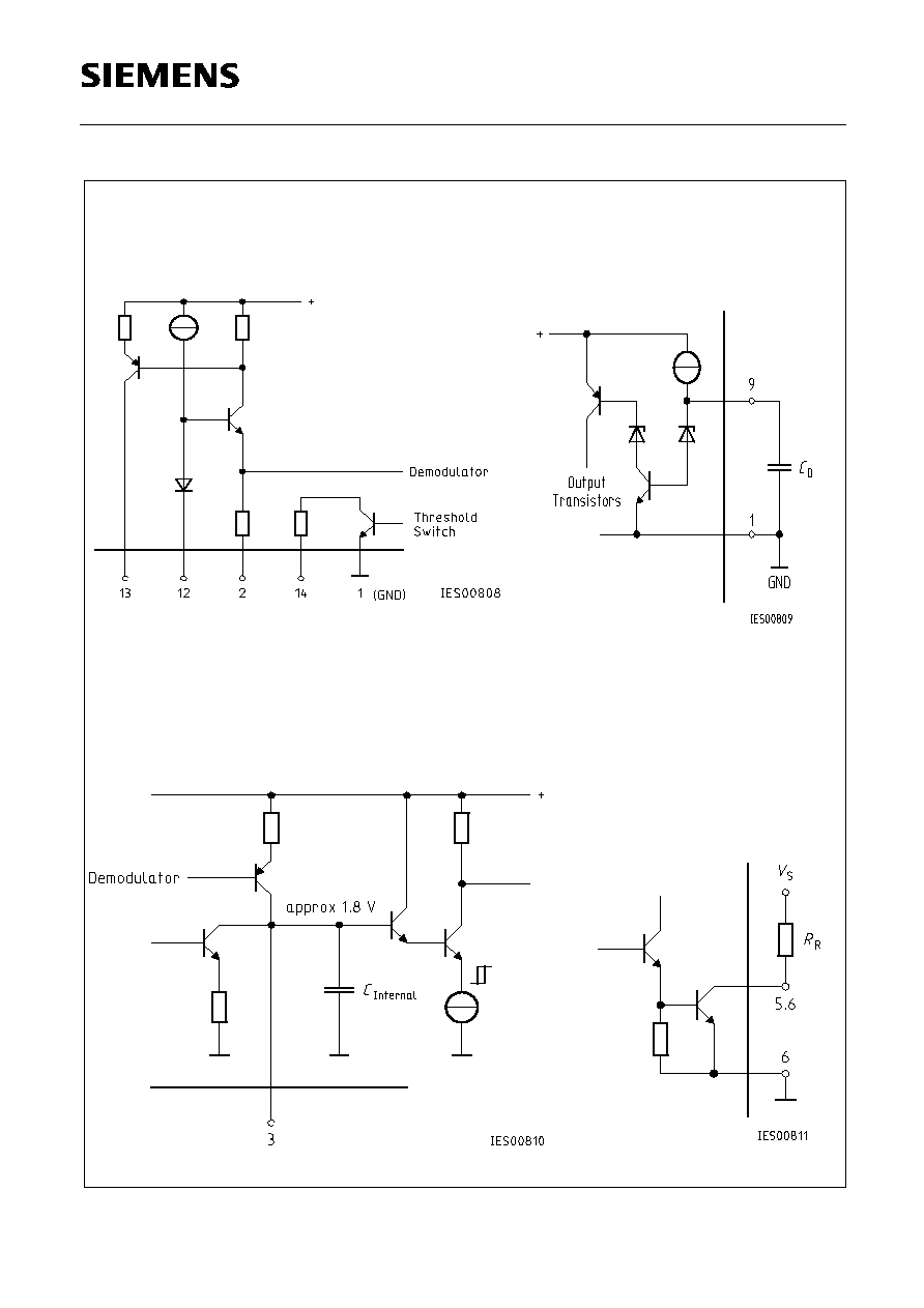
Schematic Circuit Diagram
Oscilator
Turn-ON Delay for TCA 305 A; G
Integrating Capacitor
Outputs

Semiconductor Group
6
TCA 305
TCA 355
Application Circuit
Semiconductor Group
7
TCA 305
TCA 355
L
0
,
C
0
Resonant circuit
R
Hy
Hysteresis adjustment
R
Di
Distance adjustment
D
Temperature compensation of the resonant circuit; possibly with series
resistance for the purpose of adjustment. The diode is not absolutely necessary.
Whether it is used or not depends on the temperature coefficient of the resonant
circuit.
R
I
;
C
I
Integration element. At pin 3 (integrating capacitance) we recommend a
capacitor of typ. 1 nF. To increase noise immunity this capacitor can be
substituted by an RC circuit with, e.g.,
R
I
= 1 M and
C
I
= 10 nF.
C
D
Delay capacitor
Dimensioning Examples in Accordance with CENELEC Standard (flush)
M 12
M 18
M 30
Ferrite pot core
Number of turns
Cross section of wire
L
0
C
0
(STYROFLEX
Æ
)
f
OSC
Sn
R
A
(Metal)
C
D
M 33 (7.35
◊
3.6) mm
100
0.1 CuL
206
µ
H
1000 pF
appr. 350 kHz
4 mm
8.2 k + 330
100 nF
N 22 (14.4
◊
7.5) mm
80
20
◊
0.05
268
µ
H
1.2 nF
appr. 280 kHz
8 mm
33 k
100 nF
N 22 (25
◊
8.9) mm
100
10
◊
0.1
585
µ
H
3.3 nF
appr. 115 kHz
15 mm
22 k + 2.7 k
100 nF