P-DSO-20-1
Semiconductor Group
1
04.96
Stereo Decoder/Noise Blanker
TDA 4340X
1
Overview
1.1
Features
∑ Internal reference voltage source
∑ Adjustment free oscillator with
ceramic resonator 456 kHz
∑ Pilot dependent mono/stereo switching with
hysteresis
∑ Stereo indicator output
∑ Analogue control of mono/stereo change over (stereo noise control, SNC)
∑ Pilot canceller (19 kHz)
∑ Adjacent channel noise suppression (114 kHz)
∑ MUTE facility
∑ Analogue control of deemphasis (high cut control, HCC).
∑ Stereo inputs for additional signal source at output amplifiers
∑ Interference noise detector with integrated high-pass filter
∑ (IF level signal or MPX input)
∑ MPX input low-pass filter
∑ Noise blanking at MPX demodulator outputs
∑ Input and output level adjustable (resistor values)
1.2
Application
The TDA 4340X is an integrated circuit providing the stereo decoder function and noise
blanking for FM car radio applications.
Type
Ordering Code
Package
TDA 4340X
Q67000-A5058
P-DSO-20-1
TDA 4340X
Semiconductor Group
2
04.96
1.3
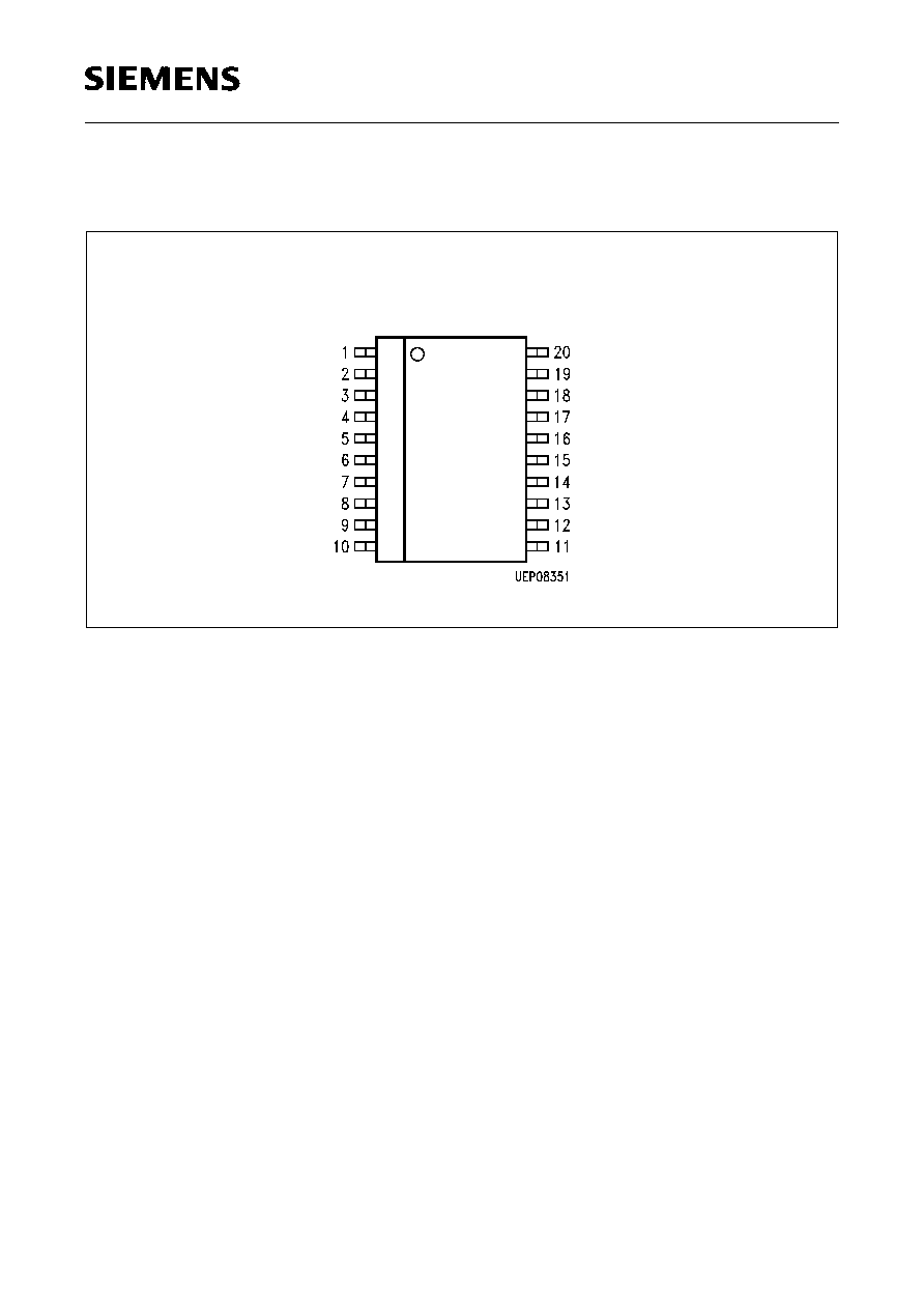
Pin Configuration
(top view)
Figure 1
P-DSO-20-1
TDA 4340X
Semiconductor Group
3
04.96
1.4
Pin Definitions and Functions
Pin No.
Function
1
Phase detector output, PLL loop filter
2
Oscillator pin (456 kHz)
3
Ground
4
Reference current pin, external reference resistor
5
Positive supply voltage
6
Interference detector input, noise detector input
7
Timing capacitor for monoflop (gate time)
Low voltage applied turns off oscillator, phase detector, pilot detector, SNC
and changes the time constant for HCC, noise gate monoflop
8
Hold capacitor for noise detector average level
Low voltage applied mutes the stereo decoder output, noise level capacitor
9
Auxiliary input left, output amplifier left
10
Audio signal output left
11
Audio signal output right
12
Auxiliary input right, output amplifier right
13
HCC timing/hold capacitor, deemphasis right
14
HCC timing/hold capacitor, deemphasis left
15
Input for HCC voltage
16
Input for SNC voltage
17
Input for reference level control voltage (HCC and SNC)
18
Pilot indicator output, open collector, active low
19
Pilot detector output
Low voltage applied switches the stereodecoder to mono state
20
Input for MPX signal
TDA 4340X
Semiconductor Group
4
04.96
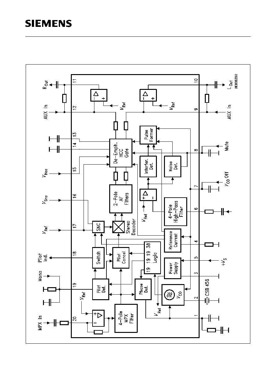
1.5
Functional Block Diagram
Figure 2
Block Diagram

TDA 4340X
Semiconductor Group
5
04.96
2
Circuit Description
Power Supply, Reference Current
A temperature stable, low noise reference voltage generator is used for better ripple
rejection and for the generation of a reference current. This current is used as a time
base for the deemphasis, the gate time of the pulse former, and the pilot cancellation,
avoiding temperature and tolerance effects.
MPX Input, MPX Filter
Adjusting the value of the input resistor, the MPX input can be adapted to the output level
of the FM demodulator. A 4-pole low-pass filter determines the bandwidth of the MPX
signal.
Voltage Controlled Oscillator, Phase Detector
The 456 kHz oscillator and the frequency dividers are used as walsh function generators
(suppression of 3rd order harmonics) for:
≠ 38 kHz for the stereo decoder
≠ 19 kHz inphase for phase detector and pilot cancellation
≠ 19 kHz quadrature for the phase detector.
The phase detector locks the on-chip 19 kHz signal to the pilot tone in the MPX signal at
90
∞
phase.
Pilot Detector, Pilot Indicator, Pilot Cancellation
The voltage at the pilot detector output is proportional to the pilot tone input level. If that
level is high enough, the pilot indicator output is activated and the pilot Cancellation
turned on: a 19 kHz signal proportional to the voltage at the pilot detector output is added
to the MPX signal with inverse polarity, cancelling the 19 kHz pilot tone.
Interference Detector, Noise Detector, Pulse Former
The signal from the interference input (MPX or field strength signal) passes a 4-pole
high-pass to the noise blanking circuitry. The average noise level is stored on an external
capacitor. The interference detector compares the actual noise level with that stored on
the capacitor and triggers the pulse former if there is a significant difference. The pulse
former generates a gate pulse for the HCC block. During that pulse time the outputs of
the deemphasis circuit are switched to hold mode.
TDA 4340X
Semiconductor Group
6
04.96
3
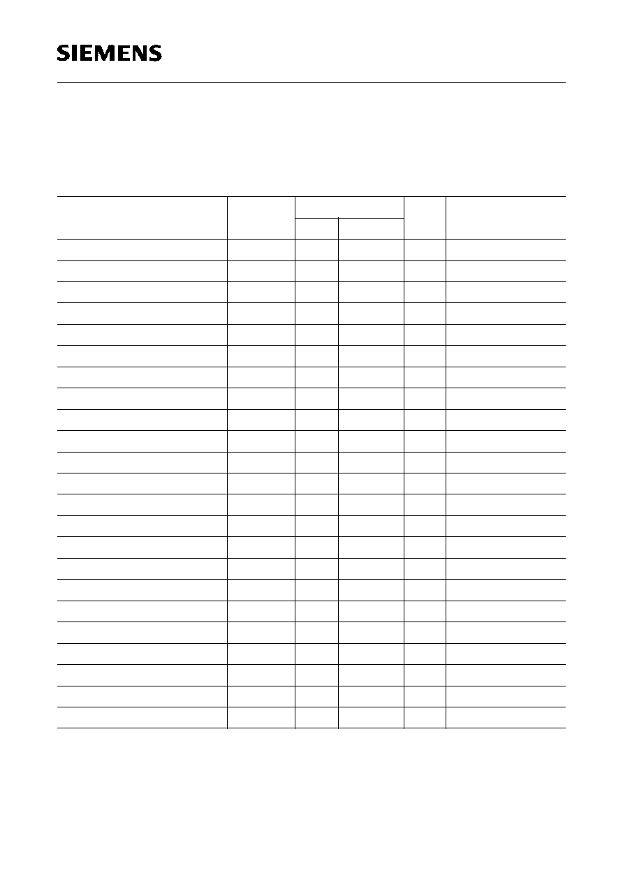
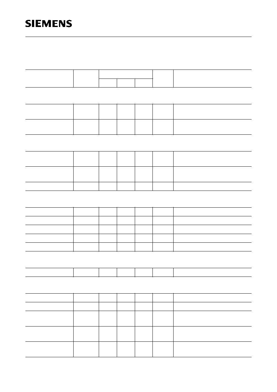
Electrical Characteristics
Note: Maximum ratings are absolute ratings; exceeding only one of these values may
cause irreversible damage to the integrated circuit.
3.1
Absolute Maximum Ratings
T
A
= ≠ 40
∞
C to 85
∞
C
Parameter
Symbol
Limit Values
Unit
Remarks
min.
max.
PLL loopfilter
V
1
0
5
V
Oscillator
I
2
≠ 1
0.1
mA
Reference current
I
4
≠ 1
0
mA
Supply voltage
V
5
0
13.2
V
Noise detector input
V
6
0
5
V
Noise gate monoflop
V
7
0
V
5
V
Noise level capacitor
V
8
0
V
5
≠ 1.5
V
Output amplifier left
V
9
0
6
V
AF output left
I
10
≠ 1
0.3
mA
AF output right
I
11
≠ 1
0.3
mA
Output amplifier right
V
12
0
6
V
Deemphasis right
V
13
0
5
V
Deemphasis left
V
14
0
5
V
HCC voltage
V
15
0
13.2
V
SNC voltage
V
16
0
13.2
V
Reference level voltage
V
17
0
13.2
V
Pilot indicator output
I
18
0
2
mA
Pilot detector output
V
19
0
V
5
≠ 1.5
V
MPX input
V
20
0
6
V
Junction temperature
T
j
≠ 40
150
∞
C
Storage temperature
T
S
≠ 40
125
∞
C
Thermal resistance
R
thSA
95
K/W
ESD voltage, HBM
V
ESD
≠ 4
4
kV
100 pF, 1500
TDA 4340X
Semiconductor Group
7
04.96
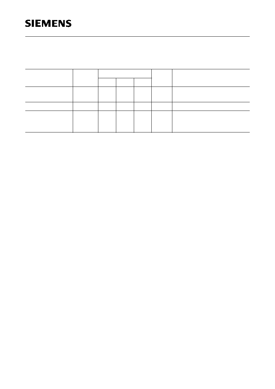
3.2
Operating Range
Note: In the operating range the functions given in the circuit description are fulfilled.
Parameter
Symbol
Limit Values
Unit
min.
max.
Supply voltage
V
S
7.5
13.2
V
Ambient temperature
T
A
≠ 40
85
∞
C
3.3
AC/DC Characteristics
V
S
= 10 V,
T
A
= 25
∞
C
Parameter
Symbol
Limit Values
Unit
Test Condition
min.
typ.
max.
Supply current
I
S
15
20
mA
Osc. ON
Supply current
I
S
10
15
mA
Osc. OFF,
V
7
= 1 V
Total harmonic
distortion
THD
0.1
0.3
%
f
= 1 kHz
Signal to noise ratio
S/N
74
80
dB
20 Hz ... 16 kHz,
Stereo
Channel separation
32
40
dB
f
= 1 kHz
MPX input level
1.7
Vpp
Overdrive margin of
input
4
8
dB
THD
= 1 %
AF output voltage
660
mVrms
f
= 1 kHz, Stereo
Overdrive margin of
output
6
9
dB
THD
= 1 %
AF output DC
voltage
2.6
3
3.4
V
Difference of output
voltage levels
1
dB
Muting depth
80
100
dB
f
= 1 kHz
DC offset at MUTE
≠ 50
0
50
mV
DC offset
stereo ON/OFF
≠ 30
0
30
mV
TDA 4340X
Semiconductor Group
8
04.96
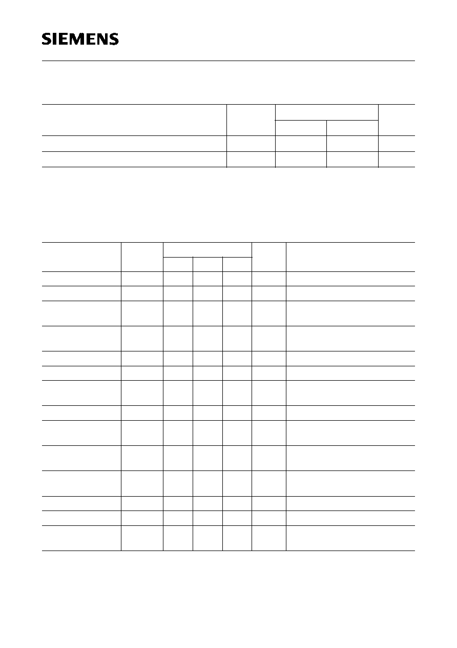
Carrier and Harmonic Suppression
Pilotsignal
subcarrier
a
19
44
50
dB
f
= 19 kHz
a
38
44
50
dB
f
= 38 kHz
a
57
1)
50
60
dB
f
= 57 kHz
a
76
1)
50
60
dB
f
= 76 kHz
Intermodulation
f
mod
= 10 kHz
a
2
1)
60
65
dB
f
S
= 2
◊
10 kHz ... 19 kHz
91 % Mono, 9 % pilot,
S
= 1 kHz
f
mod
= 13 kHz
a
3
1)
60
75
dB
f
S
= 3
◊
13 kHz ... 38 kHz
91 % Mono, 9 % pilot,
S
= 1 kHz
Traffic Radio
f
= 57 kHz
a
57
1)
70
dB
f
S
= 1 kHz
±
23 Hz
91 % Mono, 9 % pilot,
f
m
= 1 kHz,
5 % Traffic Radio Carrier
(
f
= 57 kHz,
f
m
= 23 Hz AM,
m = 60 %)
SCA (subsidiary communications authorization)
f
= 67 kHz
a
67
1)
70
dB
f
S
= 9 kHz
81 % Mono, 9 % pilot,
f
m
= 1 kHz, 10 % SCA carrier
ACI (adjacent channel interference)
f
= 119 kHz
a
114
1)
80
dB
f
= 190 kHz
a
190
1)
70
dB
Ripple rejection
1)
60
70
dB
V
5
= 10 V, 100 mVrms,
f
= 1 kHz
1)
No subject of production testing.
3.3
AC/DC Characteristics (cont'd)
V
S
= 10 V,
T
A
= 25
∞
C
Parameter
Symbol
Limit Values
Unit
Test Condition
min.
typ.
max.
TDA 4340X
Semiconductor Group
9
04.96
Mono/Stereo Control
Pilot threshold
voltage:
≠ for Stereo
ON
≠ for Stereo
OFF
≠ hysteresis
V
PIL on
V
PIL off
5
1.5
20
14
3
30
mVrms
mVrms
dB
V
PIL on
/
V
PIL off
Stereo indicator
output:
≠ Pilot OFF
≠ Pilot ON
V
18 off
I
18 on
0.5
10
V
µ
A
I
18
= 1 mA
V
18
= 13.2 V
External Control Voltages (active low)
Threshold voltage
for external mono
control (pin 19)
V
19 thr
1
1.2
V
Threshold voltage
for MUTE (pin 8)
V
8 thr
1
1.5
V
Threshold voltage
for VCO OFF (pin 7)
V
7 thr
1
1.5
V
Deemphasis
Reference voltage
V
17
0.5
4.5
V
Reference level 100 Hz
Control Range
Minimum
min
45
50
55
µ
s
V
17
= 3 V,
V
15
= 6 V,
C
deemph
= 6.8 nF
Maximum
max
135
150
165
µ
s
V
17
= 3 V,
V
15
= 0 V
C
deemph
= 6.8 nF
deemph
=
nom
V
15
V
17
V
17
= 3 V,
C
deemph
= 6.8 nF
deemph
=
1.5
◊
nom
V
15
V
17
≠
220
V
17
≠
170
V
17
≠
120
mV
V
17
= 3 V,
C
deemph
= 6.8 nF
deemph
=
2.7
◊
nom
V
15
V
17
≠
400
V
17
≠
300
V
17
≠
200
mV
V
17
= 3 V,
C
deemph
= 6.8 nF
3.3
AC/DC Characteristics (cont'd)
V
S
= 10 V,
T
A
= 25
∞
C
Parameter
Symbol
Limit Values
Unit
Test Condition
min.
typ.
max.
TDA 4340X
Semiconductor Group
10
04.96
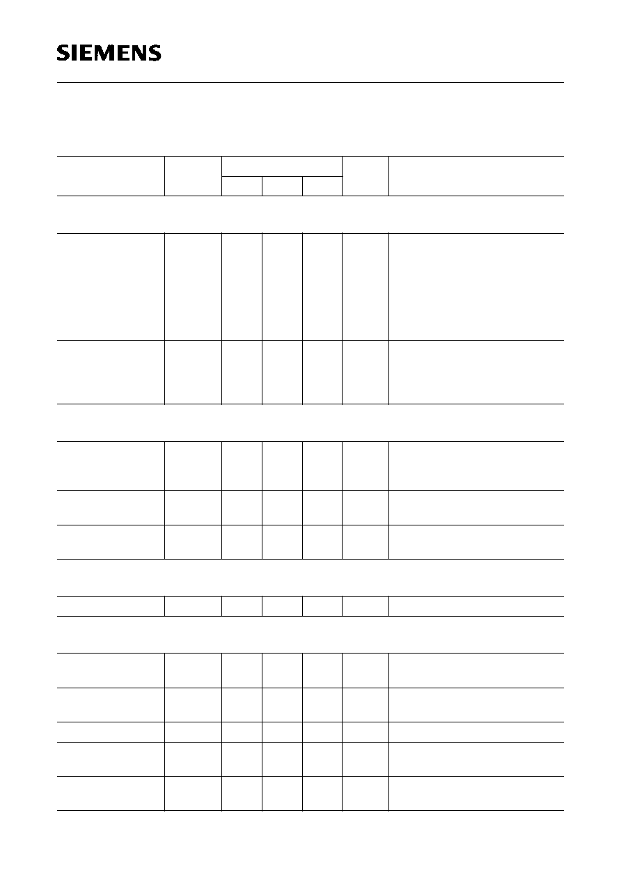
Control Range (osc. OFF)
Minimum
AM min
13
15
17
µ
s
V
17
= 3 V,
V
15
= 6 V,
V
7
= 1 V
C
deemph
= 6.8 nF
Maximum
AM max
35
40
45
µ
s
V
17
= 3 V,
V
15
= 0 V,
V
7
= 1 V
C
deemph
= 6.8 nF
Stereo/Mono Blend Control
Channel separation
V
16
V
17
≠
140
V
17
≠
115
V
17
≠
90
mV
15 dB sep.
Channel separation
V
16
V
17
≠
190
V
17
≠
170
V
17
≠
150
mV
6 dB sep.
Reference voltage
V
17
0.5
4.5
V
Oscillator
Max. osc. frequency
f
osc max
0.7
1.0
2.0
%
100%
◊
(
f
max
/456 kHz ≠ 1)
Min. osc. frequency
f
osc min
≠ 2.0
≠ 1.0
≠ 0.7
%
100%
◊
(
f
min
/456 kHz ≠ 1)
VCO gain
f
/
V
1
≠ 13
≠ 10
≠ 7
kHz/V
Oscillator voltage
V
2 DC
3
4
5
V
Oscillator swing
V
2 AC
800
1100
1400
mVpp
PLL
PD gain
i/
1)
5
7.0
9
µ
A/rad
V
pilot
= 54 mVrms
Noise Detector
Input resistance
R
6
75
100
135
k
Input high-pass filter
f
in, 6
80
100
120
kHz
≠ 3 dB
Trigger threshold
V
6 min
10
mVrms
V
8
=
V
8
(
V
6 mean
= 0),
f
6
= 200 kHz
Trigger threshold
V
6 dyn
160
mVrms
V
8
=
V
8
(
V
6 mean
= 50 mVrms),
f
6
= 200 kHz
Maximum noise
mean value
V
6maxmean
80
mVrms
f
6
= 200 kHz
3.3
AC/DC Characteristics (cont'd)
V
S
= 10 V,
T
A
= 25
∞
C
Parameter
Symbol
Limit Values
Unit
Test Condition
min.
typ.
max.
TDA 4340X
Semiconductor Group
11
04.96
Note: The listed characteristics are ensured over the operating range of the integrated
circuit. Typical characteristics specify mean values expected over the production
spread. If not otherwise specified, typical characteristics apply at
T
A
= 25
∞
C and
the given supply voltage.
Suppression pulse
duration
40
µ
s
Input offset current
I
13
,
I
14
1)
≠ 50
0
50
nA
Pulse threshold
V
6 burst
1)
130
200
mVpp
100 kHz single burst repetition
rate 100 Hz both polarities
C
in, 6
= 1 nF
1)
No subject of production testing.
3.3
AC/DC Characteristics (cont'd)
V
S
= 10 V,
T
A
= 25
∞
C
Parameter
Symbol
Limit Values
Unit
Test Condition
min.
typ.
max.
TDA 4340X
Semiconductor Group
12
04.96
Figure 3
Test Circuit

TDA 4340X
Semiconductor Group
13
04.96
Figure 4
Application Circuit
TDA 4340X
Semiconductor Group
14
04.96
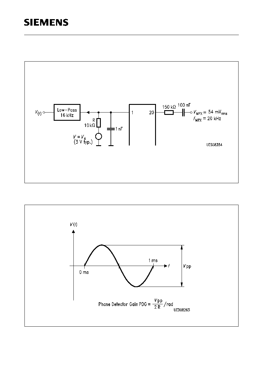
Diagrams
Figure 5
Definition of Phase Detector Gain
Figure 6
Phase Detector Gain

TDA 4340X
Semiconductor Group
15
04.96
4
Package Outlines
GPS05094
P-DSO-20-1
(Plastic Dual Small Outline Package)
Sorts of Packing
Package outlines for tubes, trays etc. are contained in our
Data Book "Package Information".
Dimensions in mm
SMD = Surface Mounted Device