P-DSO-28-1
Semiconductor Group
1
04.96
Audioprocessor
TDA 4350X
1
Overview
1.1
Features
Stereo-Soundprocessing
∑ Three stereo AF inputs, one of the inputs is
equipped with floating ground.
∑ Input level control for individual level setting of the
several AF sources in addition with a clipping
detector.
∑ Volume control with software controlled switchable loudness function. Frequency
response fixed by external components.
∑ Bass- and treble control with clipping detector.
∑ Four independent settable output attenuators for balance/fader function.
∑ Fan-out of the AF outputs software controlled.
∑ AF outputs switchable for driving bride power amplifiers.
∑
I
2
C Bus controlled immediately, or zero cross detector dependent mute, or
immediately mute via extra pin.
Control Part
∑
I
2
C Bus interface
∑ Control of sound processing
∑ Read out of the clipping detector status.
1.2
Application
The TDA 4350X is a single-chip audio-soundsystem. The circuit can be partitioned into
two functional blocks: stereo-soundprocessing and control part.
Type
Ordering Code
Package
TDA 4350X
Q67000-A5060
P-DSO-28-1
TDA 4350X
Semiconductor Group
2
04.96
1.3
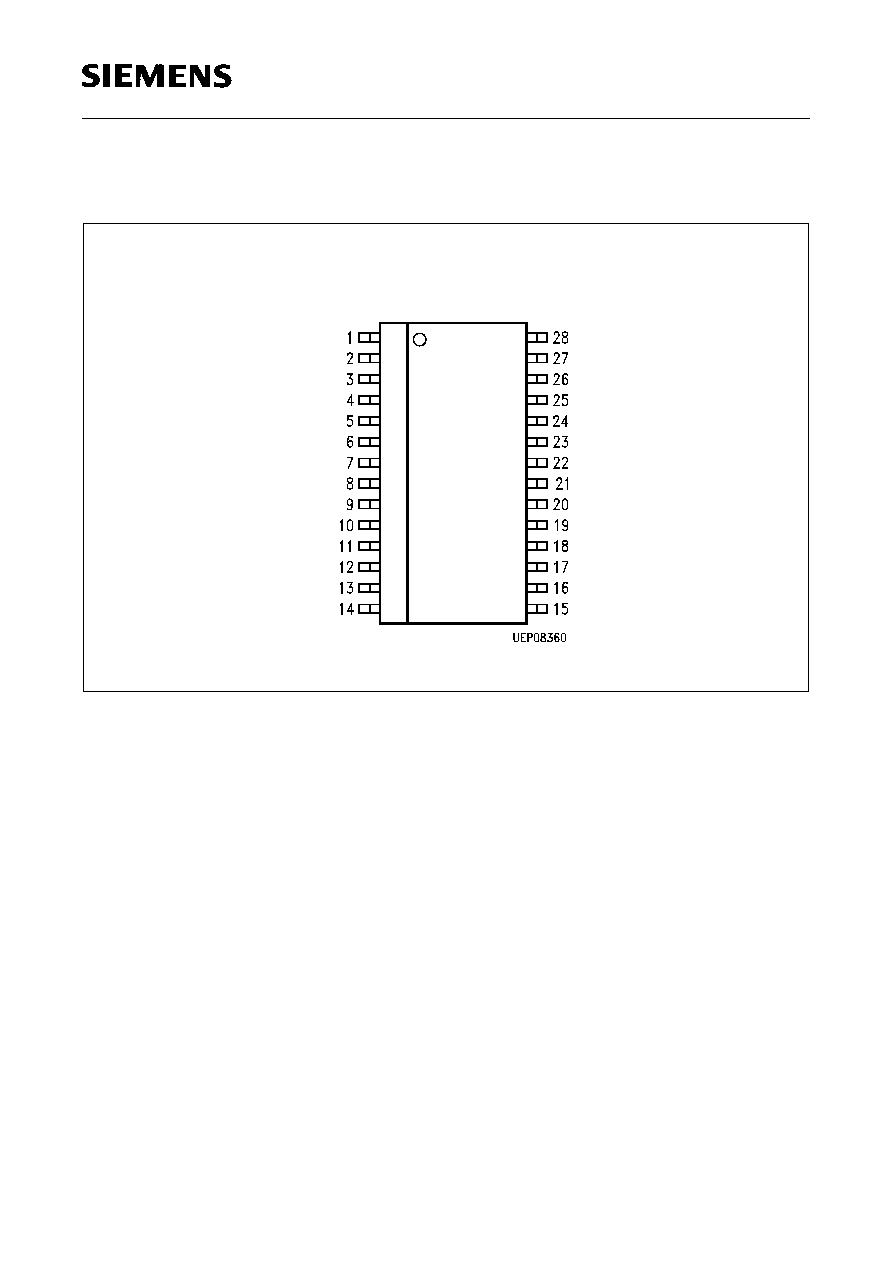
Pin Configuration
(top view)
Figure 1
P-DSO-28-1
TDA 4350X
Semiconductor Group
3
04.96
1.4
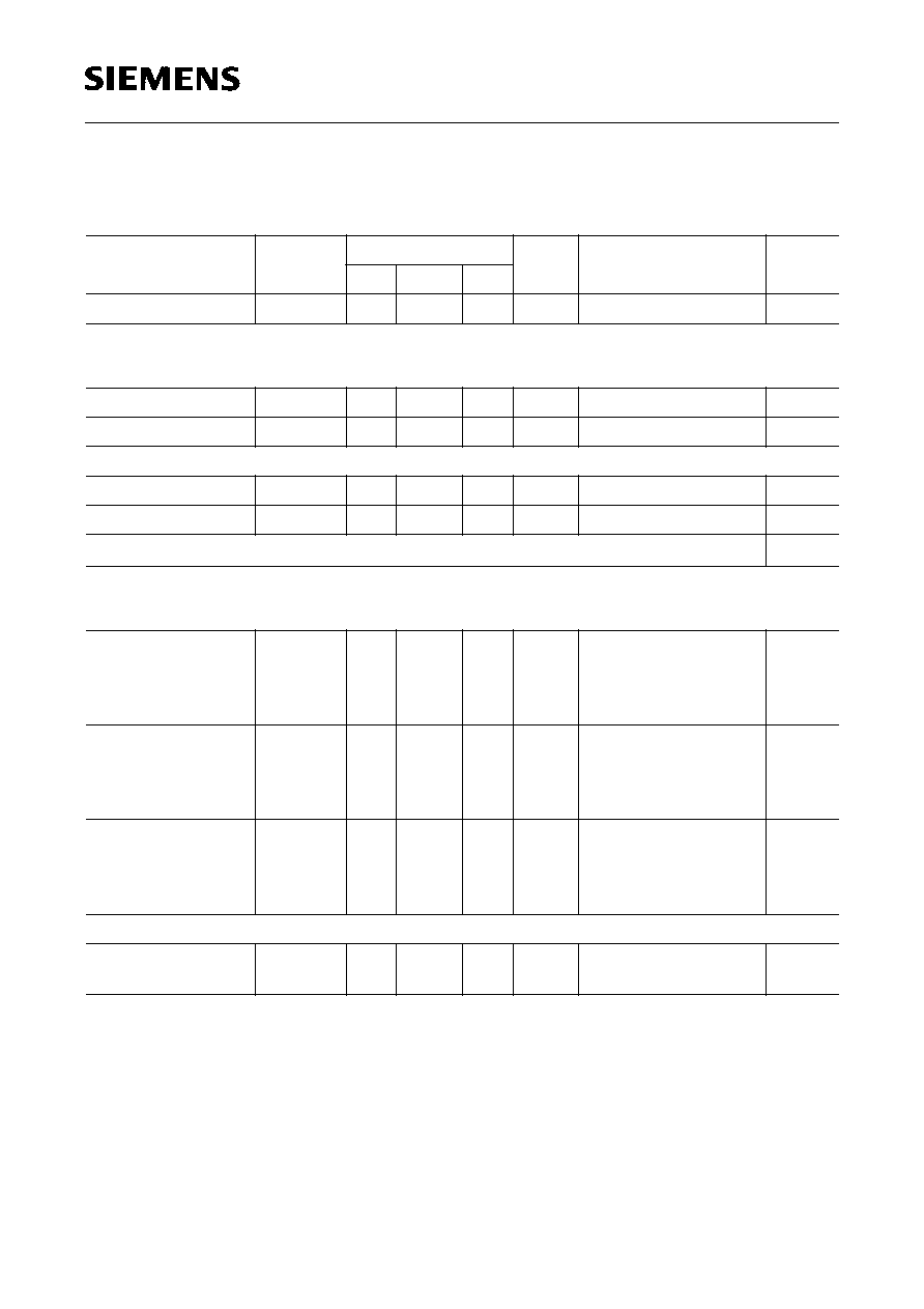
Pin Definitions and Functions
Pin No.
Function
1
CD input right
2
Input 2 right
3
Input 3 right
4
Loudness output right
5
Loudness input right
6
Digital ground
7
Mute
8
I
2
C Bus SCL
9
I
2
C Bus SDA
10
+
V
S
supply voltage
11
Corner frequency treble left
12
Corner frequency treble right
13
AF output right front
14
AF output right rear
15
AF output left rear
16
AF output left front
17
RC network bass right
18
RC network bass right
19
RC network bass left
20
RC network bass left
21
Analog ground
22
Bias for AF operation point
23
Loudness output left
24
Loudness input left
25
Input 3 left
26
Input 2 left
27
CD ground
28
CD input left
TDA 4350X
Semiconductor Group
4
04.96
1.5
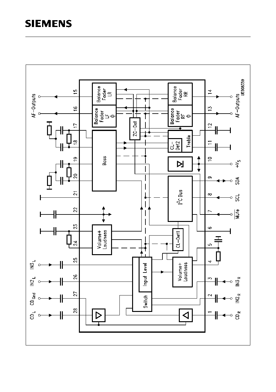
Functional Block Diagram
Figure 2
Block Diagram

TDA 4350X
Semiconductor Group
5
04.96
2
Circuit Description
2.1
Signalprocessing
1. The selection of the AF inputs happens in the input switch. There are three
stereo-inputs available. One of the input pairs is equipped with a separate floating
ground connection especially provided for external signal sources. Crosstalk to this
input is suppressed by common mode rejection. An input level control circuitry behind
input switch realizes the adaption of different signal source levels. The circuit offers a
control range from 0 dB to + 25 dB with a stepwidth of 2.5 dB. An
I
2
C Bus controlled
first clipping detector allows a software controlled level adaption.
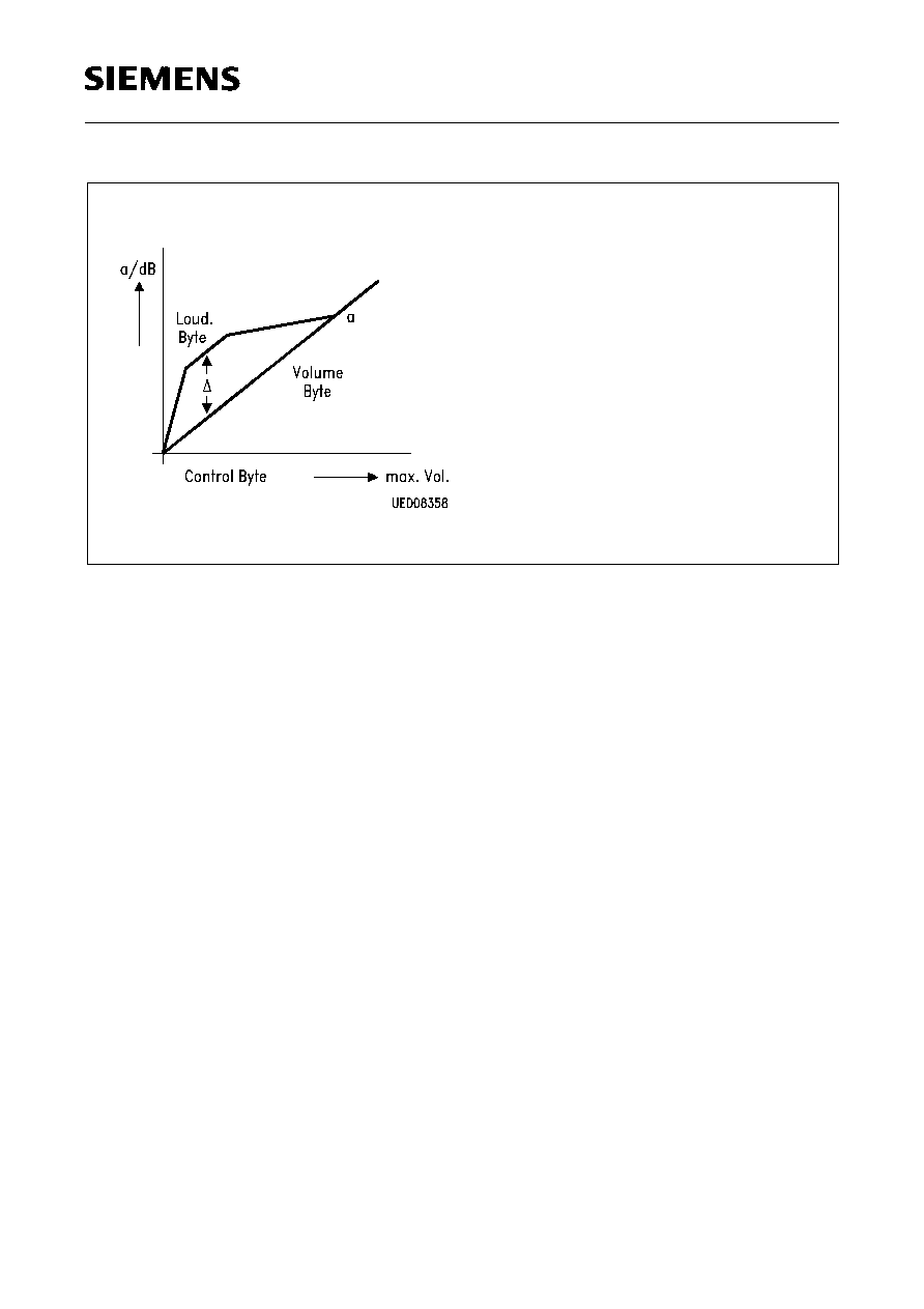
2. Next stage in signal path is volume control, with common setting for both channels, a
control range of 0 dB to ≠ 78.75 dB and a stepwidth of 1.25 dB. In this stage a
loudness function is realized. A loudness control circuit, in fact a second volume
control circuit with identical structure, is to be set to a higher level as volume control.
The resulting level difference fixes the maximum amplitude response of the loudness
function. The frequency response, only bass boost or combined bass and treble boost
is fixed by external components. Because the volume and loudness control are strictly
independent of each other, the frequency response and threshold of the loudness
function is programmable via software. A switch bit allows to enable the loudness
function easily. Some possible loudness setups:
Figure 3
Loudness function starting at max.
vol. then
continuously increasing.

TDA 4350X
Semiconductor Group
6
04.96
Figure 4
Figure 5
Loudness function starting at vol. a
then
continuously increasing.
Loudness function starting at max.
vol. increasing to
, following
constant
.
TDA 4350X
Semiconductor Group
7
04.96
Figure 6
3. In the following signalpath there is tone control, consisting of bass and treble control.
Bass control offers a control range of + 16 dB to ≠ 14 dB with a stepwidth of 2 dB.
Frequency characteristic, 1st order or 2nd order (resonance type) is fixed by external
components. Treble control also offers a control range of + 16 dB to ≠ 14 dB with a
stepwidth of 2 dB. The treble control corner frequency is determinated by an external
capacitor.
A second clipping detector allows to detect clipping in tone control part.
4. Last stages in signal path are four strictly independent controllable output attenuators
to realize balance and fader function. Each unit offers a control range of 0 dB to
≠ 38.75 dB in steps of 1.25 dB. The AF outputs are of a class A-type to avoid
distortion via software, the output fan-out can be increased to drive loads up
to
>
1.5 k
.
One output of each stereo channel can be inverted software controlled, to drive easily
bridge power amplifiers.
5. Mute control may be either done via the volume control setting, or directly for all
outputs by setting the IM (immediately mute) bit via
I
2
C Bus. The second bus
controlled mute mode is mute after signal zero crossing (ZCM). Two zero cross
detectors are built-in, therefore this mute control works independent for left and right
channel. Signal off- and on-switching is performed under zero cross detector control.
The ZCM status can be read out via
I
2
C Bus (ZCS). After activating ZCM, the ZCS
(zero crossing status) bit is set to `1', when all outputs are muted after zero crossing.
After deactivating ZCM, the ZCS bit is set to `0' when all outputs are switched on after
zero crossing. The IM mute overwrites ZCM mute. Third mute control is hardware
mute via a mute pin. If the mute pin is switched to ground all outputs are muted
immediately. Hardware mute overwrites all other mute modes.
Loudness function starting at vol. a
increasing to
, following constant
.
TDA 4350X
Semiconductor Group
8
04.96
2.2
Controlpart
All functions are controlled via an
I
2
C Bus interface. All data are stored into a latch circuit.
The telegram structure is built as follows:
Startcondition ≠ chipaddress ≠ any number of databytes ≠ stopcondition.
For the databytes the following conditions must be fulfilled:
Before transmitting a databyte a subaddress byte must first be placed in the data
telegram.
2.2.1
Chipaddress
2.2.2
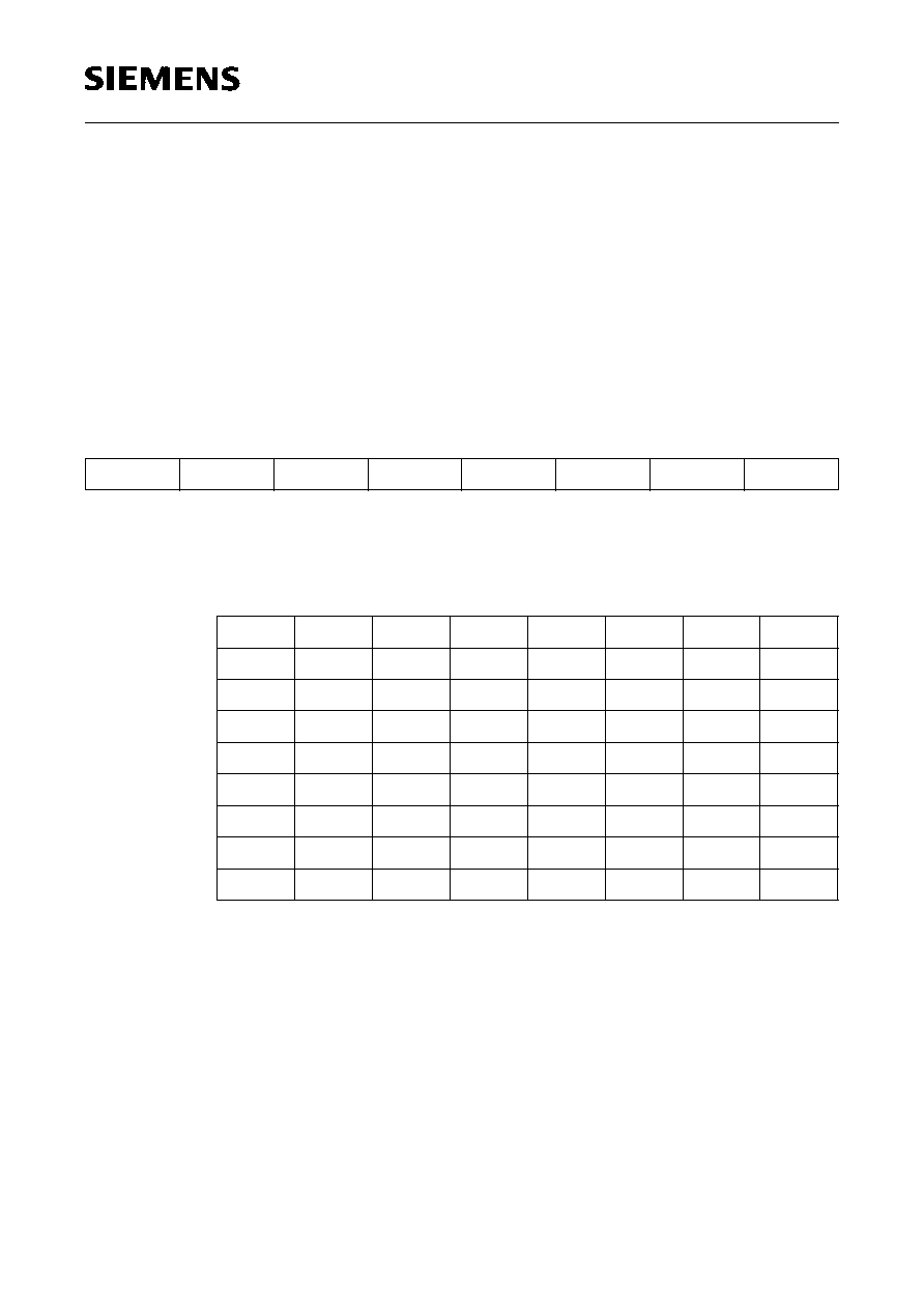
Subaddress Bytes
MSB
LSB
1
0
0
0
0
1
1
R/W
R/W = `0'
Read
R/W = `1'
Write
MSB
LSB
Switchbyte
0
0
0
0
0
0
0
0
Inputlevel
0
0
0
0
0
0
0
1
Volume
0
0
0
0
0
0
1
0
Loudness
0
0
0
0
0
0
1
1
Bass/Treble
0
0
0
0
0
1
0
0
Out rear left
0
0
0
0
0
1
0
1
Out front left
0
0
0
0
0
1
1
0
Out rear right
0
0
0
0
0
1
1
1
Out front right
0
0
0
0
1
0
0
0
TDA 4350X
Semiconductor Group
9
04.96
2.2.3
Control Bytes
a) Switch Control Byte
b) Input Level Control Byte
MSB
LSB
ZCM
IM
Fan
Ph
IN-3
IN-2
IN-CD
X
IN-CD = `0'
IN-CD = `1'
CD input OFF; power ON
CD input ON
IN-2 = `0'
IN-2 = `1'
Input 2 OFF; power ON
Input 2 ON
IN-3 = `0'
IN-3 = `1'
Input 3 OFF; power ON
Input 3 ON
If no input is selected, mute function is active.
If no protection against multiple selection implemented!
Ph = `0'
Ph = `1'
Bridgepower amplifier operation ON; power ON
Normal operation
Fan = `0'
Fan = `1'
Normal operation; power ON
Increased Fan out ON
IM = `0'
IM = `1'
Normal operation; power ON
Immediate mute for all AF outputs
ZCM = `0'
ZCM = `1'
Normal operation; power ON
Mute after signal zero crossing
IM overwrites ZCM, handware mute overwrites all other mute modes.
MSB
LSB
Min. gain
X
X
X
X
0
0
0
0
Min. gain + 1
X
X
X
X
0
0
0
1
power ON
Max. gain ≠ 1
X
X
X
X
1
0
0
1
Max. gain
X
X
X
X
1
0
1
0
to
Max. gain
X
X
X
X
1
1
1
1
TDA 4350X
Semiconductor Group
10
04.96
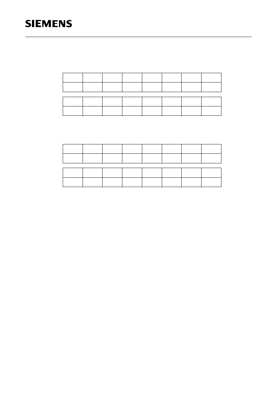
c) Volume Level Control Byte
d) Loudness Control Byte
MSB
LSB
Min. gain
X
0
0
0
0
0
0
0
Min. gain + 1
X
0
0
0
0
0
0
1
power ON
Max. gain ≠ 1
X
0
1
1
1
1
1
0
Max. gain
X
0
1
1
1
1
1
1
MSB
LSB
Min. gain
X
Ld
0
0
0
0
0
0
Min. gain + 1
X
Ld
0
0
0
0
0
1
power ON
Max. gain ≠ 1
X
Ld
1
1
1
1
1
0
Max. gain
X
Ld
1
1
1
1
1
1
Ld = `0'
Loudness OFF; power ON
(loudness attenuator has the same setting
as volume attenuator)
Ld = `1'
Loudness ON

TDA 4350X
Semiconductor Group
11
04.96
e) Treble/Bass Control Byte
f ) Output Control Bytes
MSB
LSB
linear
1
0
0
0
1
0
0
0
max. treble,
lin. bass
0
0
0
0
1
0
0
0
min. treble,
lin. bass
1
1
1
1
1
0
0
0
lin. treble,
max. bass
1
0
0
0
0
0
0
0
lin. treble,
min. bass
1
0
0
0
1
1
1
1
max. treble,
max. bass
0
0
0
0
0
0
0
0
min. treble,
min. bass
1
1
1
1
1
1
1
1
power ON
0
0
0
0
0
0
0
1
treble
bass
MSB
LSB
Min. gain
X
X
X
X
0
0
0
0
Min. gain + 1
X
X
X
X
0
0
0
1
power ON
Max. gain ≠ 1
X
X
X
X
1
1
1
0
Max. gain
X
X
X
X
1
1
1
1

TDA 4350X
Semiconductor Group
12
04.96
2.2.4
Talkmode
Figure 7
AF Inputs Pin 1/2/3/25/26/27/28
MSB
LSB
CI1
CI2
ZCS
X
X
X
X
X
CI1 = `0'
CI1 = `1'
CL 2 = `0'
CL2 = `1'
ZCS = `0'
ZCS = `1'
Normal operation
Input level control output at clipping level
Normal operation
Tone control output at clipping level
All AF outputs are ON after ZCS set to `0'
All AF outputs are muted after ZCM set to `1'

TDA 4350X
Semiconductor Group
13
04.96
Figure 8
AF Outputs Pin 13/14/15/16
Figure 9
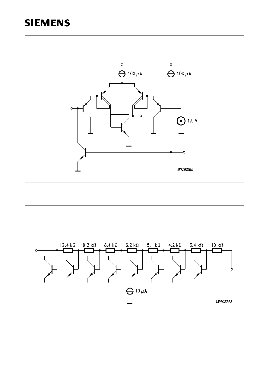
Mute Pin 7,
I
2
C Bus SCL Pin 8
TDA 4350X
Semiconductor Group
14
04.96
Figure 10
I
2
C Bus SDA Pin 9
Figure 11
Corner Frequency Treble Pin 11/12
TDA 4350X
Semiconductor Group
15
04.96
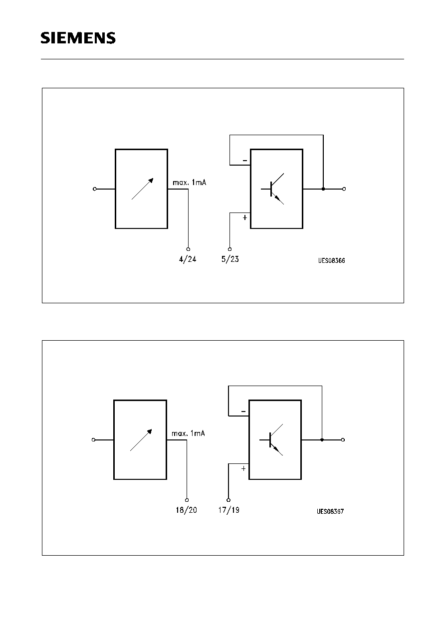
Figure 12
Loudness Pin 4/5/23/24
Figure 13
RC Network Bass Pin 17/18/19/20
TDA 4350X
Semiconductor Group
16
04.96
Figure 14
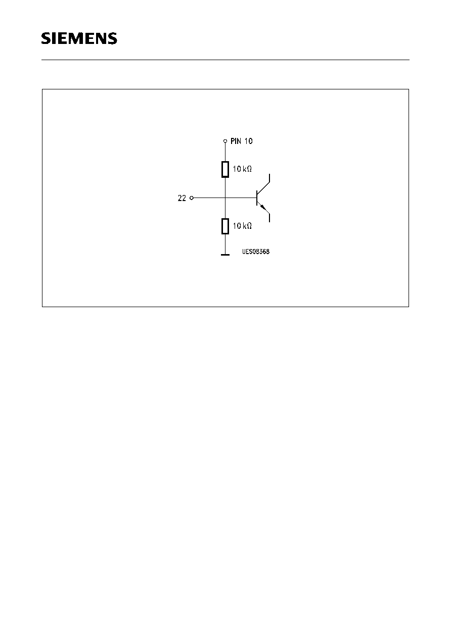
Bias for AF Operation Point Pin 22

TDA 4350X
Semiconductor Group
17
04.96
3
Electrical Characteristics
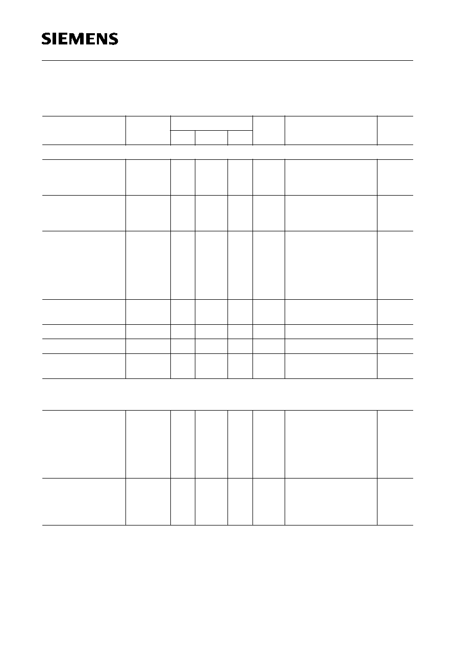
3.1
Absolute Maximum Ratings
T
A
= ≠ 40
∞
C to 85
∞
C
Parameter
Symbol
Limit Values
Unit Remarks
min.
max.
Supply voltage
V
10
0
14
V
Max. DC voltage
V
1
0
V
10
V
Max. DC voltage
V
2
0
V
10
V
Max. DC voltage
V
3
0
V
10
V
Max. DC voltage
V
5
0
V
10
V
Max. DC voltage
V
7
0
V
10
V
Max. DC voltage
V
8
0
V
10
V
Max. DC voltage
V
9
0
V
10
V
Max. DC voltage
V
11
0
V
10
V
Max. DC voltage
V
12
0
V
10
V
Max. DC voltage
V
17
0
V
10
V
Max. DC voltage
V
19
0
V
10
V
Max. DC voltage
V
22
0
V
10
V
Max. DC voltage
V
23
0
V
10
V
Max. DC voltage
V
25
0
V
10
V
Max. DC voltage
V
26
0
V
10
V
Max. DC voltage
V
27
0
V
10
V
Max. DC voltage
V
28
0
V
10
V
Max. DC current
I
4
0
2
mA
Max. DC current
I
13
0
5
mA
Max. DC current
I
14
0
5
mA
Max. DC current
I
15
0
5
mA
Max. DC current
I
16
0
5
mA
Max. DC current
I
18
0
2
mA
Max. DC current
I
20
0
2
mA
Max. DC current
I
24
0
2
mA
TDA 4350X
Semiconductor Group
18
04.96
Note: Maximum ratings are absolute ratings; exceeding only one of these values may
cause irreversible damage to the integrated circuit.
3.2
Operational Range
Note: In the operating range the functions given in the circuit description are fulfilled.
Junction temperature
T
j
150
∞
C
Storage temperature
T
g
125
∞
C
Thermal resistance
R
thSA
76
K/W
ESD voltage, HBM
V
ESD1
≠ 4
4
kV
1.5 k
,
100 pF
ESD voltage, AF outputs
V
ESD2
≠ 6
6
kV
1.5 k
,
100 pF
Parameter
Symbol
Limit Values
Unit
min.
max.
Supply voltage
V
S
7.5
13.2
V
Ambient temperature range
T
A
≠ 40
85
∞
C
Input frequency range
f
I
0.01
20
kHz
3.1
Absolute Maximum Ratings (cont'd)
T
A
= ≠ 40
∞
C to 85
∞
C
Parameter
Symbol
Limit Values
Unit Remarks
min.
max.
TDA 4350X
Semiconductor Group
19
04.96
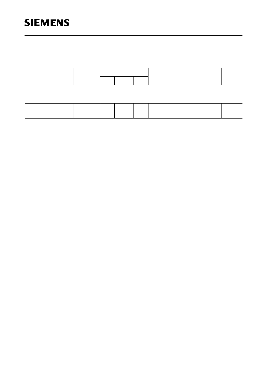
3.3
AC/DC Characteristics
V
10
= 10 V;
T
A
= 25
∞
C
Parameter
Symbol
Limit Values
Unit
Test Condition
Test
Circuit
min. typ.
max.
Current consumption
I
10
45
mA
1
Signal Section
Gain
G
13-1
0
dB
1
Gain
G
14-1
0
dB
1
Analogous values are apply for feeding in on pins 2 and 3.
Gain
G
15-28
0
dB
1
Gain
G
16-28
0
dB
1
Analogous values are apply for feeding in on pins 25 and 26.
Input Level Control
Min. gain
G
13-1
G
14-1
G
15-28
G
16-28
0
dB
1
Max. gain
G
13-1
G
14-1
G
15-28
G
16-28
25
dB
01,0A
V
inp
10
1
Stepwidth
G
13-1
G
14-1
G
15-28
G
16-28
2.5
dB
01,X-01, X
±
1
V
inp
X-V
inp
(X
±
1)
1
Analogous values are apply for feeding in on pins 2, 3, 25 and 26.
Threshold
Clipping detector 1
V
1 CI1
V
28 CI1
1.9
Vrms
1

TDA 4350X
Semiconductor Group
20
04.96
Volume Control
Max. gain
G
13-1
G
14-1
G
15-28
G
16-28
0
dB
1
Min. gain
G
13-1
G
14-1
G
15-28
G
16-28
≠ 78.25
dB
02,00; 03,00
Vol. 0; Loud. OFF
1
Tracking error
G
13-14
G
15-16
G
13-16
G
14-15
±
2
dB
02,3F-02,24; 03,3F
Vol. 63-36; Loud. OFF
1
Stepwidth
G
13
G
14
G
15
G
16
1.25
dB
02,X-02, (X
±
1)
Vol. X-Vol. (X
±
1)
1
Loudness Control
Max. gain
G
4-1
G
24-28
≠ 6
dB
03,7F; 02,00
Loud. ON
1
Min. gain
G
4-1
G
24-28
≠ 84.75
dB
03,40; 02,00
Loud. 0
1
Tracking error
G
5-24
±
2
dB
03,7F-03,64; 02,00
Loud. 63-36; Loud. ON
1
Stepwidth
G
4
G
24
1.25
dB
03,X-03, (X
±
1)
Loud. X-Loud. (X
±
1)
1
3.3
AC/DC Characteristics (cont'd)
V
10
= 10 V;
T
A
= 25
∞
C
Parameter
Symbol
Limit Values
Unit
Test Condition
Test
Circuit
min. typ.
max.

TDA 4350X
Semiconductor Group
21
04.96
Output Control
Max. gain
G
13-1
G
14-1
G
15-28
G
16-28
0
dB
1
Min. gain
G
13-1
G
14-1
G
15-28
G
16-28
≠ 38.75
dB
08,00; Out 0
07,00; Out 0
05,00; Out 0
06,00; Out 0
1
Stepwidth
G
13
G
14
G
15
G
16
1.25
dB
08,X-08, (X
±
1)
OutX-Out (X
±
1)
07,X-07, (X
±
1)
OutX-Out (X
±
1)
05,X-05, (X
±
1)
OutX-Out (X
±
1)
06,X-06, (X
±
1)
OutX-Out (X
±
1)
1
3.3
AC/DC Characteristics (cont'd)
V
10
= 10 V;
T
A
= 25
∞
C
Parameter
Symbol
Limit Values
Unit
Test Condition
Test
Circuit
min. typ.
max.

TDA 4350X
Semiconductor Group
22
04.96
Bass Control
Bass boost
G
13-1
G
14-1
G
15-28
G
16-28
14
16
dB
04,80;
f
1
= 40 Hz
Bass min, Treble lin
1
Bass cut
G
13-1
G
14-1
G
15-28
G
16-28
≠ 14
dB
04,8F;
f
1
= 40 Hz
Bass min, Treble lin
1
Bass stepwidth
G
13
G
14
G
15
G
16
1
2
3
dB
04,8X (X
±
1)
BassX-Bass (X
±
1)
1
Treble Control
Treble boost
G
13-1
G
14-1
G
15-28
G
16-28
14
16
dB
04,80;
f
1
= 15 kHz
Treble max, Bass lin
1
Treble cut
G
13-1
G
14-1
G
15-28
G
16-28
≠ 14
dB
04,8F;
f
1
= 15 kHz
Treble min, Bass lin
1
Treble stepwidth
G
13
G
14
G
15
G
16
1
2
3
dB
04,8X-04, (X
±
1) 8
TrebleX-Treble (X
±
1)
1
Tone linearity
G
13
G
14
G
15
G
16
1
2
3
dB
04, 88-04,
f
1
= 40 Hz ... 15 kHz
Treble, Bass lin
1
Threshold
clipping detector 2
V
1 CI2
V
28 CI2
380
mVrms 04,00
f
1
= 40 Hz or 15 kHz
Treble max, Bass max
1
3.3
AC/DC Characteristics (cont'd)
V
10
= 10 V;
T
A
= 25
∞
C
Parameter
Symbol
Limit Values
Unit
Test Condition
Test
Circuit
min. typ.
max.

TDA 4350X
Semiconductor Group
23
04.96
Channel separation
G
14-15
G
13-16
80
dB
V
1
or
V
28
= 300 mVrms 1
Analogous values apply for feeding on pins 2, 3, 25 and 26.
Crosstalk
attenuation input
switch
a
in use/out interf.
80
dB
V
i use.
= 0
V
i interf.
= 300 mVrms
1
Feed on pins 1-3 and 25, 26, 28, measured on pins 13-16.
Attenuation mute
a
1-13
a
1-14
a
28-15
a
28-16
80
dB
02,7F;
V
1
= 300 mVrms
mute active
00,20;
V
1
= 300 mVrms
notselect
02,7F;
V
28
= 300 mVrms
mute active
00,20;
V
28
= 300 mVrms
notselect
1
Max. input voltage
V
1
V
28
2
2
Vrms
Vrms
THD
13
<
1 %
THD
14
<
1 %
THD
15
<
1 %
THD
16
<
1 %
1
1
Max. output voltage
V
13
V
14
V
15
V
16
2.2
Vrms
THD
13
<
1 %
01,07;
V
inp.
7
THD
14
<
1 %
01,07;
V
inp.
7
THD
15
<
1 %
01,07;
V
inp.
7
THD
16
<
1 %
01,07;
V
inp.
7
1
Distortion
THD
13
THD
14
THD
15
THD
16
0.01
0.05
%
V
1
= 300 mVrms
V
28
= 300 mVrms
1
3.3
AC/DC Characteristics (cont'd)
V
10
= 10 V;
T
A
= 25
∞
C
Parameter
Symbol
Limit Values
Unit
Test Condition
Test
Circuit
min. typ.
max.

TDA 4350X
Semiconductor Group
24
04.96
Analog values apply for feeding in on pins 2, 3, 25 and 26.
Distortion
THD
13
THD
14
THD
15
THD
16
0.01
0.1
%
V
1
= 300 mVrms
02,2F; 03,6F;
Vol. 47
V
28
= 300 mVrms
02,2F; 03,6F;
Vol. 47
1
Distortion
THD
13
THD
14
THD
15
THD
16
0.05
0.2
%
V
1
= 150 mVrms 04,XX
any tone setting
V
28
= 150 mVrms 04,XX
any tone setting
1
Unweighted
signal/noise ratio
a
S
/
N
13
a
S
/
N
14
a
S
/
N
15
a
S
/
N
16
105
dB
V
Nrms 20 Hz ... 20 kHz
V
1
= 2 Vrms
V
Nrms 20 Hz ... 20 kHz
V
28
= 2 Vrms
1
Unweighted
signal/noise ratio
a
S
/
N
13
a
S
/
N
14
a
S
/
N
15
a
S
/
N
16
60
dB
V
Nrms 20 Hz ... 20 kHz
V
1
= 0.3 Vrms
02,27; 03,67
Vol. 39
V
Nrms 20 Hz ... 20 kHz
V
28
= 0.3 Vrms
02,27; 03,67
Vol. 39
1
Unweighted noise
voltage
V
N13
V
N14
V
N15
V
N16
20
µ
Vrms
V
Nrms 20 Hz ... 20 kHz
02,00; 03,00
Vol. 0
1
Bridge power-amp
13-14
180
Bit Ph = `0'
1
Modus
15-16
180
Bit Ph = `0'
1
Load resistor
R
L13, 14
R
L15, 16
R
L13, 14
R
L15, 16
4.5
1.5
k
k
V
13, 14
= 2.5 V;
THD
<
1 %
V
15, 16
= 2.5 V;
THD
<
1 %
Bit fan = `1'
V
13, 14
= 2.5 V;
THD
<
1 %
Bit fan = `1'
V
15, 16
= 2.5 V;
THD
<
1 %
1
1
DC jump
1 bit
V
13
±
4
mV
Sub, X-Sub, X
±
1
1
3.3
AC/DC Characteristics (cont'd)
V
10
= 10 V;
T
A
= 25
∞
C
Parameter
Symbol
Limit Values
Unit
Test Condition
Test
Circuit
min. typ.
max.
TDA 4350X
Semiconductor Group
25
04.96
Analog values apply for measuring on pins 14, 15 and 16.
DC jump
1 bit
V
13
±
6
mV
01, 03-01, 04-01,
05-01, 06-01, 07
Input level control
1
DC jump
1 bit
V
13
±
10
mV
01, 07-01, 08-01,
09-01, 0A-01, 08
Input level control
1
PSRR
Power supply
Ripple rejection
a
PSRR13
a
PSRR14
a
PSRR15
a
PSRR16
70
70
70
70
dB
dB
dB
dB
V
i interf.
= 1 Vrms
f
i interf.
= 100 Hz
...
20 kHz
R
G
= 220
R
G
= 220
Measurement
CCIR 651 Effective
1
1
1
1
Zero crossing
detector window
±
30
mV
1
Mute active
V
QML
0.3
1.5
V
1
Mute inactive
V
QMH
3
5.5
V
1
Input current
I
QH
I
QL
50
100
µ
A
µ
A
1
1
Design Hints
Input resistance
R
1
R
2
R
3
R
25
R
26
R
28
30
k
Output resistance
R
13
R
14
R
15
R
16
70
3.3
AC/DC Characteristics (cont'd)
V
10
= 10 V;
T
A
= 25
∞
C
Parameter
Symbol
Limit Values
Unit
Test Condition
Test
Circuit
min. typ.
max.
TDA 4350X
Semiconductor Group
26
04.96
I
2
C Bus (SCL, SDA)
SCL, SDA Edges
Rise time
t
R
1
µ
s
Fall time
t
F
300
ns
Shift Register Clock Pulse SCL
Frequency
f
SCL
0
100
kHz
H pulse width
t
High
4
µ
s
L pulse width
t
Low
4
µ
s
Start
Set-up time
t
SUSTA
4
µ
s
Hold time
t
HDSTA
4
µ
s
Stop
Set-up time
t
SUSTO
4
µ
s
Bus free time
t
BUF
4
µ
s
Data Transfer
Set-up time
t
SUDAT
250
ns
Hold time
t
HDDAT
1
µ
s
Input SCL, SDA
Input voltage
V
QH
V
QL
3
5.5
1.5
V
1
Input current
I
QH
I
QL
3
50
100
µ
A
µ
A
1
3.3
AC/DC Characteristics (cont'd)
V
10
= 10 V;
T
A
= 25
∞
C
Parameter
Symbol
Limit Values
Unit
Test Condition
Test
Circuit
min. typ.
max.
TDA 4350X
Semiconductor Group
27
04.96
Note: The listed characteristics are ensured over the operating range of the integrated
circuit. Typical characteristics specify mean values expected over the production
spread. If not otherwise specified, typical characteristics apply at
T
A
= 25
∞
C and
the given supply voltage.
Output SDA (open collector)
Output voltage
V
QH
V
QL
5.5
0.4
V
R
L
= 2.5 k
I
QL
= 3 mA
1
3.3
AC/DC Characteristics (cont'd)
V
10
= 10 V;
T
A
= 25
∞
C
Parameter
Symbol
Limit Values
Unit
Test Condition
Test
Circuit
min. typ.
max.

TDA 4350X
Semiconductor Group
28
04.96
Figure 15
Test Circuit

TDA 4350X
Semiconductor Group
29
04.96
Application Circuit 1
Figure 16
Bass Loudness Circuitry and Bass Control Resonance Characteristic

TDA 4350X
Semiconductor Group
30
04.96
Application Circuit 2
Figure 17
Bass/Treble Loudness Circuitry and 1. Order Bass Control Characteristic
TDA 4350X
Semiconductor Group
31
04.96
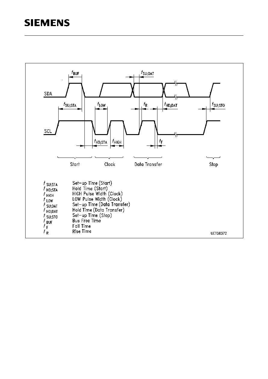
Diagram
Figure 18
I
2
C Bus Timing
TDA 4350X
Semiconductor Group
32
04.96
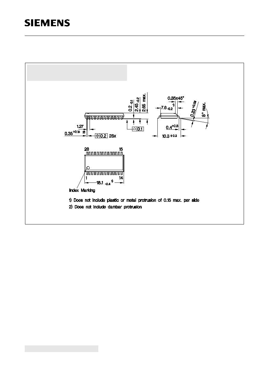
4
Package Outlines
P-DSO-28-1
(Plastic Dual Small Outline Package)
GPS05123
Sorts of Packing
Package outlines for tubes, trays etc. are contained in our
Data Book "Package Information".
Dimensions in mm
SMD = Surface Mounted Device