Functional Description and Application
This integrated circuit permits the design of TV-tuners covering the entire frequency
range from 48 ... 900 MHz split into 2 parts with 3 frequency bands.
The application is suitable for all tuners in TV-and VCR-sets.
Circuit Description
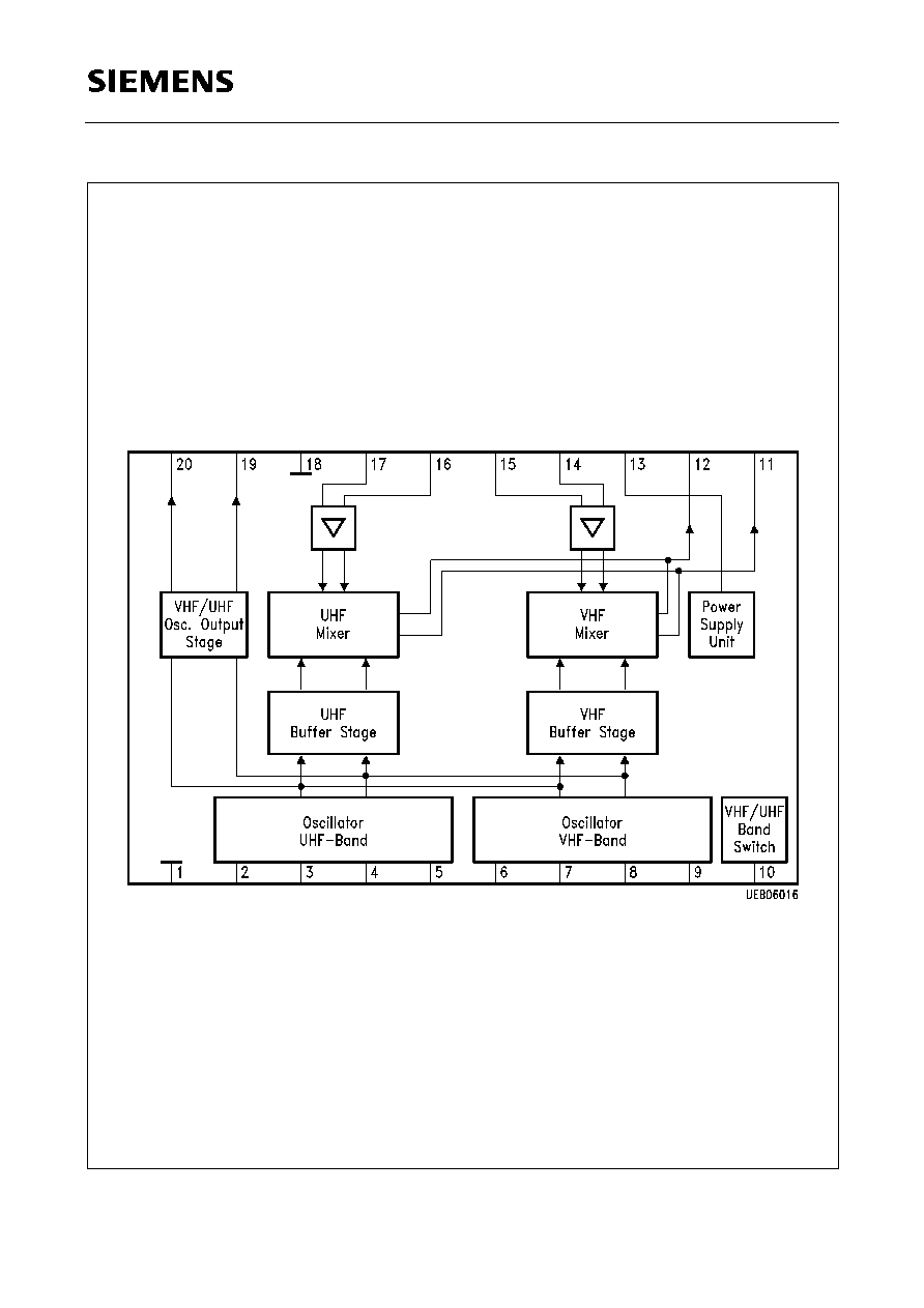
This IC includes 2 balanced mixers (double balanced mixer/ring mixer), two balanced
oscillators for VHF (I and II) and UHF, a reference voltage source and band switch.
Filters between tuner input and IC separate the TV-frequency signal into two bands. The
band switch ensures that only one band at a time is activated. In the activated band the
signal passes a frontend stage with MOSFET-amplifier, a double-tuned bandpass filter
and is then fed to the activated balanced mixer input of the IC which is a low-impedance
stage for the VHF- and UHF-range, respectively.
The input signal is mixed there with the oscillator signal from the activated oscillator
section and fed to a common IF-stage for all bands.
Type
Ordering Code
Package
MTI 3006X
Q67000-A5152
P-DSO-20-1 (SMD)
MTI 3006X
Q67006-A5152
P-DSO-20-1 Tape & Reel (SMD)
VHF/UHF-Tuner IC
Bipolar IC
MTI 3006X
P-DSO-20-1
Features
q
Few external components
q
Frequency and amplitude-stable balanced oscillator
for VHF (I and II) and UHF
q
Mixer stages with optimized suppression of
oscillator and input frequency at IF-output
q
Mixer with low intermodulation if large input signals
are applied
q
Balanced mixer with wide dynamic range and
low-impedance inputs
q
Internal band switch
q
Low-noise, internal reference voltage
Semiconductor Group
1
12.94

Semiconductor Group
2
MTI 3006X
Pin Configuration
(top view)
Pin Definitions and Functions
Pin No. Symbol
Function
1
GND
Ground
2
UHF Osc. Input 1
UHF-oscillator amplifier, high-impedance base input,
symmetrical to pin 5
3
UHF Osc. Output 1
UHF-oscillator amplifier, high-impedance collector
output, symmetrical to pin 4
MTI 3006X
Semiconductor Group
3
4
UHF Osc. Output 2
UHF-oscillator amplifier, high-impedance collector
output, symmetrical to pin 3
5
UHF Osc. Input 2
UHF-oscillator amplifier, high-impedance base input,
symmetrical to pin 2
6
VHF Osc. Input 1
VHF-oscillator amplifier, high-impedance base input,
symmetrical to pin 9
7
VHF Osc. Output 1
VHF-oscillator amplifier, high-impedance collector
output, symmetrical to pin 8
8
VHF Osc. Output 2
VHF-oscillator amplifier, high-impedance collector
output, symmetrical to pin 7
9
VHF Osc. Input 2
VHF-oscillator amplifier, high-impedance base input,
symmetrical to pin 6
10
Band Switching
VHF/UHF-band switching
11
Mixer Output 1
Open collector mixer output, high-impedance,
symmetrical to pin 12
12
Mixer Output 2
Open collector mixer output, high-impedance,
symmetrical to pin 11
13
+
V
S
Supply voltage
14
VHF Input 1
VHF-mixer input low-impedance, symmetrical to pin 15
15
VHF Input 2
VHF-mixer input low-impedance, symmetrical to pin 14
16
UHF Input 1
UHF-mixer input low-impedance, symmetrical to pin 17
17
UHF Input 2
UHF-mixer input low-impedance, symmetrical to pin 16
18
GND
Ground
19
Osc. Output 1
VHF/UHF-oscillator signal output to PLL, symmetrical to
pin 20
20
Osc. Output 2
VHF/UHF-oscillator signal output to PLL, symmetrical to
pin 19
Pin Definitions and Functions (cont'd)
Pin No. Symbol
Function
Semiconductor Group
4
MTI 3006X
Block Diagram

MTI 3006X
Semiconductor Group
5
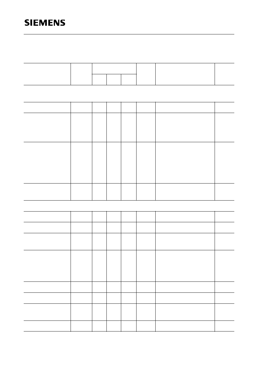
Absolute Maximum Ratings
T
A
= 0 to 70
∞
C
Parameter
Symbol
Limit Values
Unit
min.
max.
Supply voltage
V
11, 12, 13
≠
0.3
14.5
V
Switching voltage
V
10
≠
0.3
V
S
V
According to the test circuit 1, only the provided circuitry can be connected to pins 1 to
9 and 14 to 20
Junction temperature
T
j
150
∞
C
Storage temperature
T
stg
≠
40
125
∞
C
Thermal resistance
R
th
125
K/W
Operating Range
Supply voltage
V
S
10
13.2
V
VHF-mixer input
frequency range
f
VHF
30
500
MHz
UHF-mixer input
frequency range
f
UHF
30
900
MHz
VHF-oscillator
frequency range
f
OVHF
30
500
MHz
UHF-oscillator
frequency range
f
OUHF
30
900
MHz
Ambient temperature
T
A
0
70
∞
C

Semiconductor Group
6
MTI 3006X
AC/DC Characteristics
T
A
= 25
∞
C;
V
S
= 12 V
Parameter
Symbol
Limit Values
Unit
Test Condition
Test
Circuit
min.
typ.
max.
Current consumption
I
13
20
28
36
mA
V
10
> 1.6 V
1
Oscillator output
impedance
R
19, 20
C
19, 20
200
2
pF
Parallel equivalent circuit
Parallel equivalent circuit
2
2
Mixer output
impedance
R
11, 12
C
11, 12
10
2
k
pF
Parallel equivalent circuit
Parallel equivalent circuit
2
2
VHF-Circuit Section
Switching voltage
V
10
1.6
2.3
V
1
Switching current
I
10
10
30
µ
A
V
10
= 2.1 V
1
Oscillator frequency
range
f
VHF I
f
VHF II
80
140
170
450
MHz
MHz
V
d
= 0 ... 28 V
V
d
= 0 ... 28 V
1
Oscillator drift
f
VHF
f
VHF
f
VHF
200
400
200
kHz
kHz
kHz
V
S
= 12 V
±
10 %
T
= 25
∞
C
t
= 5 s to 15 min.
after switching on
1
1
1
Oscillator level
V
19, 20
≠ 17
≠ 14
≠ 11
dBm
voltage on 50
1
Harmonic wave ratio
a
H
10
15
dB
1
Crosstalk
f
in
/LO
V
14/15
150
1000
mVrms max. input level for
10-dB distance
f
in
/LO
1
Mixer gain
G
VHF
11
14
17
dB
1
Mixer noise figure
F
VHF I
F
VHF II
6.5
7.5
11
11
dB
dB
VHF 1; DSB
VHF 2; DSB
1
Mixer input
impedance
R
14/15
L
14/15
25
10
nH
serial equivalent circuit
serial equivalent circuit
1
1
MTI 3006X
Semiconductor Group
7
VHF-Circuit Section (cont'd)
(Design Hints only)
IF-suppression
a
IF
20
dB
V
14/15
= 80 dB
µ
V
1
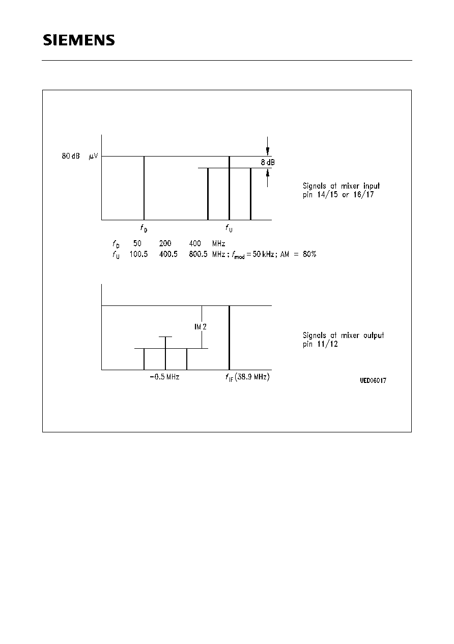
IM2
a
IM2
a
IM2
60
60
70
67
dB
dB
f
D
= 50 MHz
f
U
= 100.5 MHz
f
D
= 200 MHz
f
U
= 400.5 MHz
3
3
IM3
a
IM3
a
IM3
60
60
65
64
dB
dB
f
D
= 100 MHz
f
U1
= 150 MHz
f
U2
= 160 MHz
f
D
= 200 MHz
f
U1
= 250 MHz
f
U2
= 260 MHz
4
4
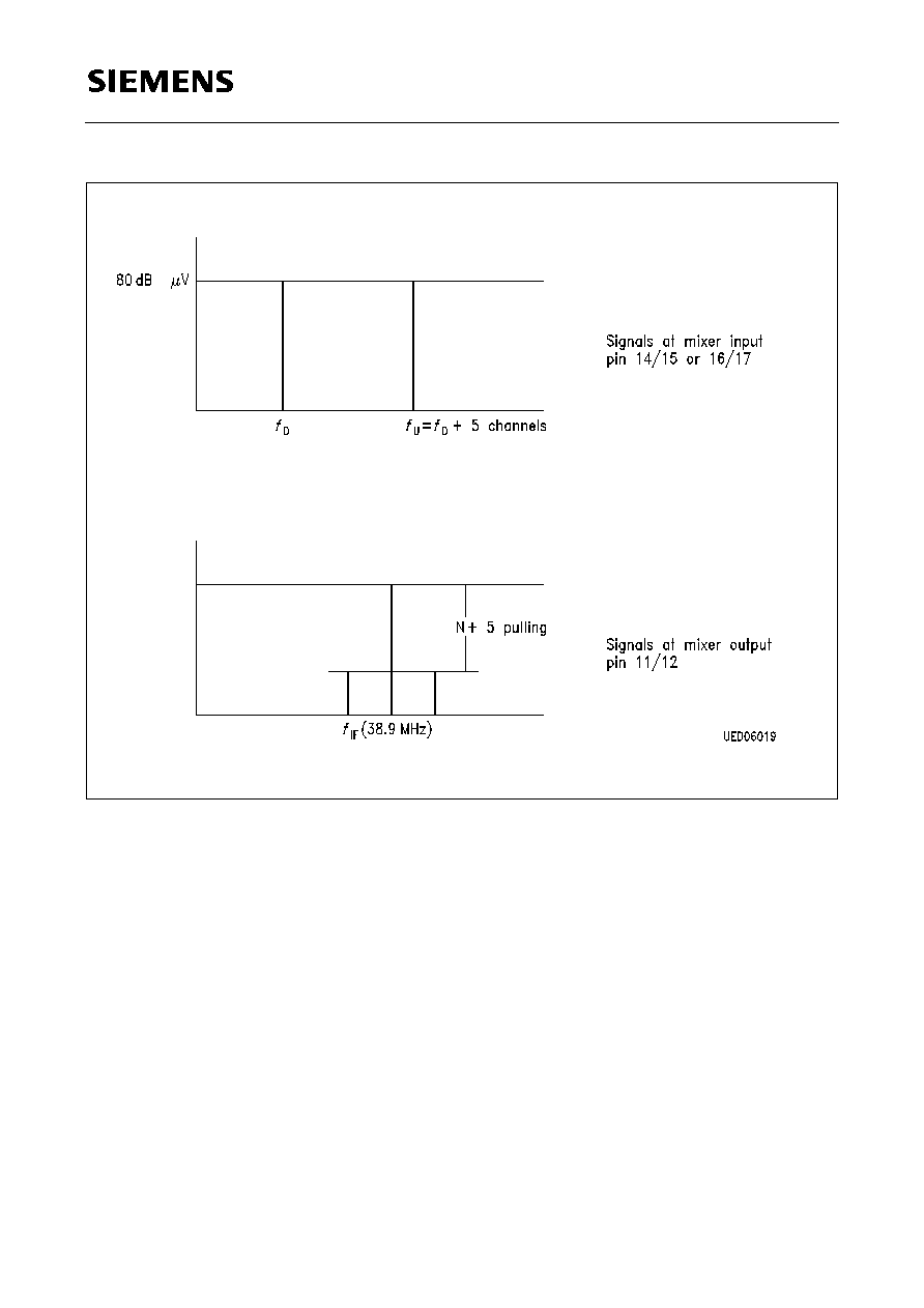
N + 5 pulling
a
N + 5
a
N + 5
50
50
60
60
dB
dB
f
D
= 50 MHz
f
D
= 200 MHz
5
5
UHF-Circuit Section
Switching voltage
V
10
3.2
V
S
V
1
Switching current
I
10
60
300
µ
A
V
10
=
V
S
1
Oscillator frequency
range
f
UHF
440
900
MHz
V
d
= 0 ... 28 V
1
Oscillator drift
f
UHF
f
UHF
f
UHF
400
800
200
kHz
kHz
kHz
V
S
= 12 V
±
10 %
T
= 25
∞
C
t
= 5 s to 15 min.
after switching on
1
1
1
Oscillator level
V
19, 20
≠ 22
≠ 17
≠ 13
dBm
voltage on 50
1
Harmonic wave ratio
a
H
10
20
dB
1
Crosstalk
f
in
/LO
V
16/17
150
1000
mVrms
max. input level for
10-dB distance
f
in
/LO
1
Mixer gain
G
UHF
11
14
17
dB
1
AC/DC Characteristics (cont'd)
T
A
= 25
∞
C;
V
S
= 12 V
Parameter
Symbol
Limit Values
Unit
Test Condition
Test
Circuit
min.
typ.
max.

Semiconductor Group
8
MTI 3006X
Mixer noise figure
F
UHF
8
12
dB
DSB
1
Mixer input
impedance
R
16/17
L
16/17
25
10
nH
serial equivalent circuit
serial equivalent circuit
2
2
UHF-Circuit Section (cont'd)
(Design Hints only)
IF-suppression
a
ZF
20
dB
V
16/17
= 80 dB
µ
V
1
IM2
a
IM2
60
61
dB
f
D
= 400 MHz
f
U
= 800.5 MHz
3
IM3
a
IM3
a
IM3
60
60
66
70
dB
dB
f
D
= 600 MHz
f
U1
= 650 MHz
f
U2
= 660 MHz
f
D
= 850 MHz
f
U1
= 800 MHz
f
U2
= 790 MHz
4
4
N + 5 pulling
a
N + 5
a
N + 5
50
50
60
60
dB
dB
f
D
= 500 MHz
f
D
= 800 MHz
5
5
AC/DC Characteristics (cont'd)
T
A
= 25
∞
C;
V
S
= 12 V
Parameter
Symbol
Limit Values
Unit
Test Condition
Test
Circuit
min.
typ.
max.
MTI 3006X
Semiconductor Group
9
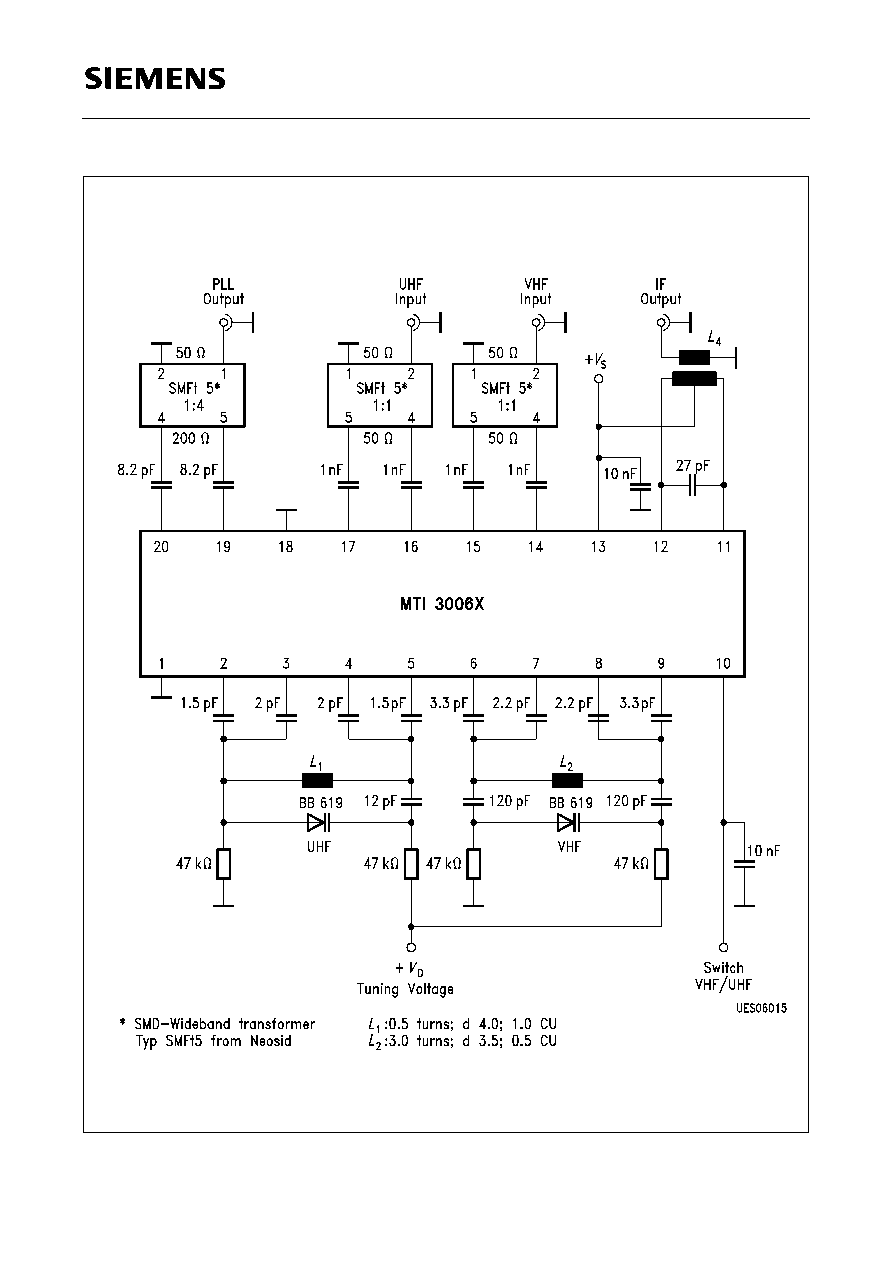
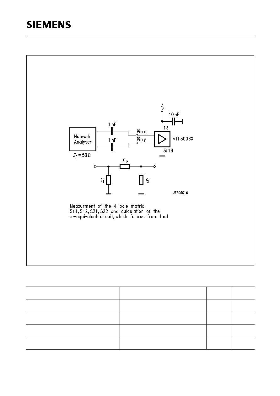
Test Circuit 1
Semiconductor Group
10
MTI 3006X
Test Circuit 2
Test Point
Test Frequency in MHz
Pin x
Pin y
Oscillator output impedance
100
19
20
Mixer input impedance VHF
100
14
15
Mixer input impedance UHF
600
17
18
Mixer output impedance VHF/UHF 100/600
11
12
MTI 3006X
Semiconductor Group
11
Test Circuit 3
IM2 (
f
U
≠
f
D
) Transfer to
f
IF

Semiconductor Group
12
MTI 3006X
Test Circuit 4
IM3 (
f
U2
≠
f
U1
) Transfer to
f
IF
±
(
f
U2
≠
f
U1
)
MTI 3006X
Semiconductor Group
13
Test Circuit 5
N + 5 Pulling

Semiconductor Group
14
MTI 3006X
Package Outline
Plastic Package, P-DSO-20-1 (SMD)
(Plastic Dual Small Outline Package)
GPS05094
Sorts of Packing
Package outlines for tubes, trays etc. are contained in our
Data Book "Package Information"
Dimensions in mm
SMD = Surface Mounted Device