Decoder for Program Delivery
Control and Video Program System
PDC / VPS Decoder
CMOS IC
P-DIP-14-3
P-DSO-20-1
Features
q
Single-chip receiver for PDC data, broadcast either
≠ in Broadcast Data Service Packet (BDSP) 8/30/2
according to CCIR teletext system B, or
≠ in dedicated line no. 16 of the vertical blanking interval
(VPS)
q
Reception of Unified Date and Time (UDT) broadcast in
BDSP 8/30/1
q
Low external components count
q
On-chip data and sync slicer
q
I
2
C-Bus interface for communication with external
microcontroller
q
Selection of PDC/VPS operating mode software controlled
by
I
2
C-Bus register
q
Pin and software compatible to VPS Decoder SDA 5642
q
Supply voltage: 5 V
±
10 %
q
Video input signal level: 0.7 Vpp to 1.4 Vpp
q
Technology: CMOS
q
Package: P-DIP-14-3 and P-DSO-20-1
q
Operating temperature range: 0 to 70
∞
C
Semiconductor Group
21
12.94
SDA 5648
SDA 5648X
Functional Description
The CMOS circuit SDA 5648 is intended for use in video cassette recorders to retrieve control data
of the PDC system from the data lines broadcast during the vertical blanking interval of a standard
video signal.
The SDA 5648 is devised to handle PDC data transported either in Broadcast Data Service Packet
(BDSP) 8/30 format 2 (bytes no. 13 through 25) of CCIR teletext system B or in the dedicated data
line no. 16 in the case of VPS.
Furthermore it is able to receive the Unified Date and Time (UDT) information transmitted in bytes
no. 15 through 21 of packet 8/30 format 1.
Type
Ordering Code
Package
SDA 5648
Q67000-A5186
P-DIP-14-3
SDA 5648X
Q67006-A5198
P-DSO-20-1 Tape & Reel
SDA 5648
SDA 5648X
Semiconductor Group
22
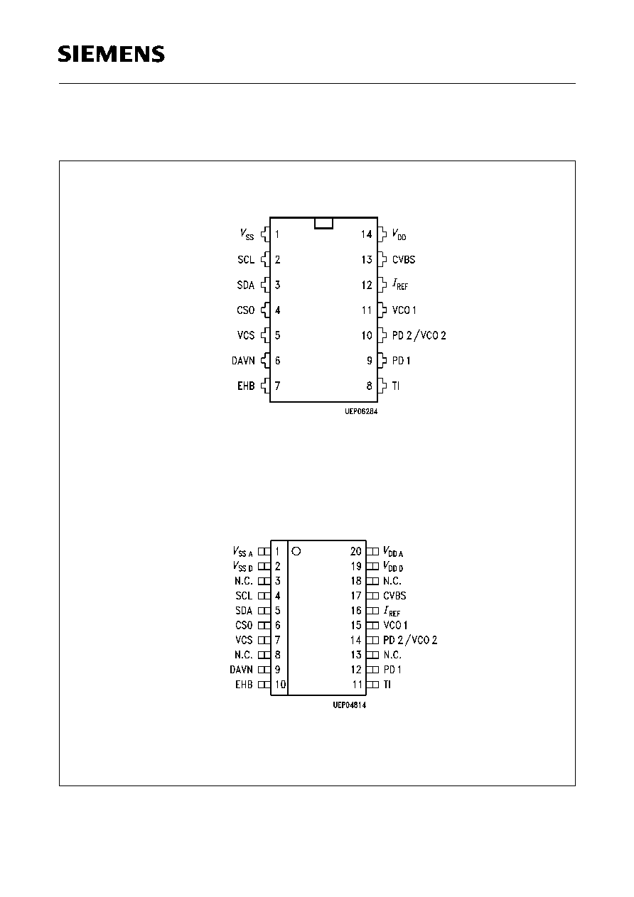
Pin Configuration
(top view)
Operating mode (PDC/VPS) is selected by a control register which can be written to via the
I
2
C-Bus
interface.
P-DIP-14-3
P-DSO-20-1

SDA 5648
SDA 5648X
Semiconductor Group
23
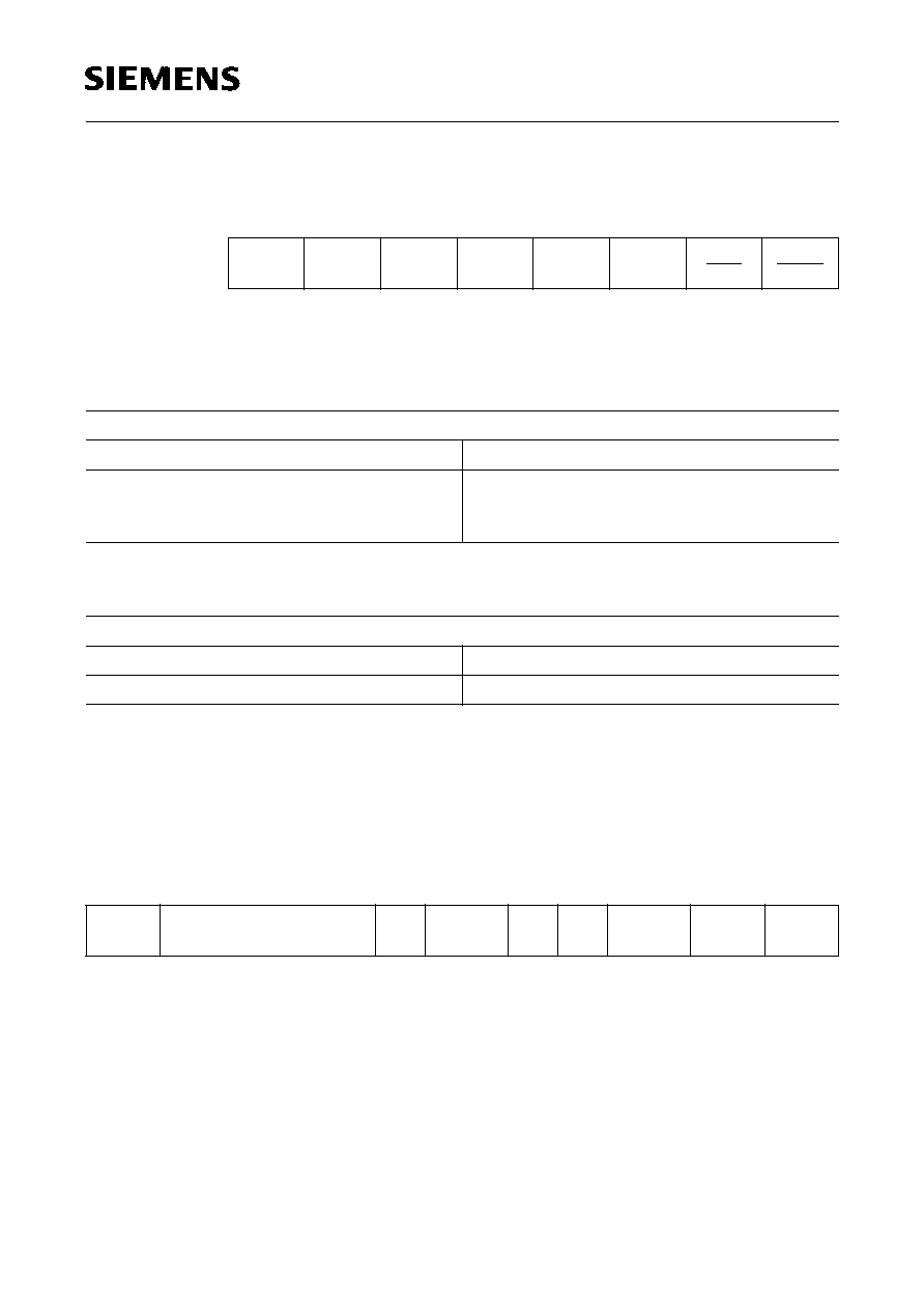
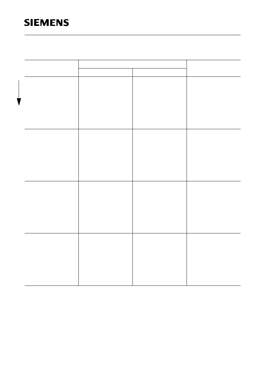
Pin Definitions and Functions
Pin No.
P-DIP-14-3
Pin No.
P-DSO-20-1
Symbol
Function
1
V
SS
Ground (0 V)
1
V
SSA
Analog ground (0 V)
2
V
SSD
Digital ground (0 V)
3
N.C.
Not connected
2
4
SCL
Serial clock input of
I
2
C-Bus.
3
5
SDA
Serial data input of
I
2
C-Bus.
4
6
CS0
Chip select input determining the
I
2
C-Bus addresses:
20
H
/ 21
H
, when pulled low
22
H
/ 23
H
, when pulled high.
5
7
VCS
Video Composite Sync output from sync slicer used for
PLL based clock generation.
8
N.C.
Not connected
6
9
DAVN
Data available output active low, when PDC/VPS data
is received.
7
10
EHB
Output signaling the presence of the first field active
high.
8
11
TI
Test input; activates test mode when pulled high.
9
12
PD1
Phase detector/charge pump output of data PLL
(DAPLL).
13
N.C.
Not connected
10
14
PD2/VCO2
Connector of the loop filter for the SYSPLL.
11
15
VCO1
Input to the voltage controlled oscillator #1 of the
DAPLL.
12
16
I
REF
Reference current input for the on-chip analog circuit.
13
17
CVBS
Composite video signal input.
18
N.C.
Not connected
14
V
DD
Positive supply voltage (+ 5 V nom.).
19
V
DDD
Positive supply voltage for the digital circuits
(+ 5 V nom.).
20
V
DDA
Positive supply voltage for the analog circuits
(+ 5 V nom.).
SDA 5648
SDA 5648X
Semiconductor Group
24
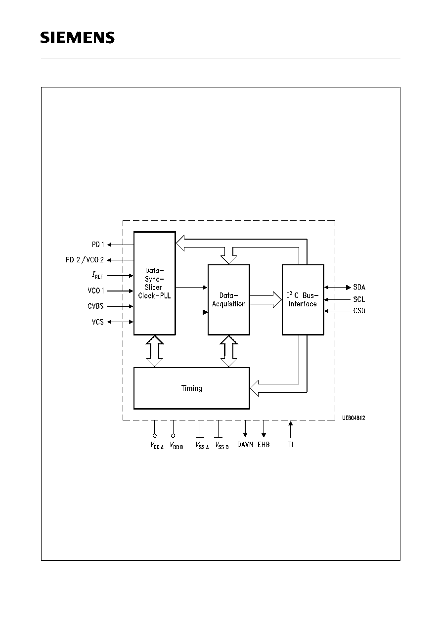
Block Diagram

SDA 5648
SDA 5648X
Semiconductor Group
25
Circuit Description
Referring to the functional block diagram of the PDC / VPS decoder, the composite video signal with
negative going sync pulses is coupled to the pin CVBS through a capacitor which is used for
clamping the bottom of the sync pulses to an internally fixed level. The signal is passed on to the
slicer, an analog circuitry separating the sync and the data parts of the CVBS signal, thus yielding
the digital composite sync signal VCS and a digital data signal for further processing by comparing
those signals to internally generated slicing levels.
The output of the sync separator is forwarded, on one hand, to the output pin VCS, and on the other
hand, to the clock generator and the Timing block. The VCS signal represents a key signal that is
used for deriving a system clock signal by means of a PLL.
The data slicer separates the data signal from the CVBS signal by comparing the video voltage to
an internally generated slicing level which is found by averaging the data signal during TV line no.
16 in the VPS mode or by averaging the data signal during the clock run-in period of the teletext
lines during the data entry window (DEW) in PDC mode.
The clock generator delivers the system clock needed for the basic timing as well as for the
regeneration of the data clock. It is based on two phase locked loops (PLL's) all parts of which are
integrated on chip with the exception of the loop filter components. Each of the PLL's is composed
of a voltage controlled oscillator (VCO), a phase/frequency detector (PFD), and a charge pump
which converts the digital output signals of the PFD to an analog current. That current is
transformed to a control voltage for the VCO by the off-chip loop filter. The generated VCO fre-
quencies are 10 MHz and 13.875 MHz for VPS mode and PDC mode, respectively.
All signals necessary for the control of sync and data slicing as well as for the data acquisition are
generated by the Timing block.
In PDC mode, only teletext rows 8/30 containing Broadcast Data Service Package (BDSP) infor-
mation are acquired. The relevant bytes of 8/30 format 1 (8/30/1) and 8/30 format 2 (8/30/2) are
extracted. The 8/30/1-bytes are stored in the acquisition register in a transparent way without any
bit manipulation, whereas the Hamming coded bytes of packet 8/30/2 are Hamming-checked and
bytes with one bit error are corrected. The storage of error free or corrected 8/30/2-data bytes in the
transfer register to the
I
2
C-Bus is signalled by the DAVN output going low. The reception and
storage of 8/30/1- data, however, is not indicated by the DAVN output. The presence of 8/30/1 data
can only be checked by polling the data register via the
I
2
C-Bus.
In VPS mode, the extracted data bits of TV line no. 16 are checked for biphase errors. With no
biphase errors encountered, the acquired bytes are stored in the transfer register to the
I
2
C-Bus.
That transfer is signalled by a H/L transition of the DAVN output, as well.
In both operating modes data are updated when a new data line has been received, provided that
the chip is not accessed via the
I
2
C-Bus at the same time.
A micro controller can read the stored bytes via the
I
2
C-Bus interface at any time. However, one
must be aware that the storage of new data from the acquisition interface is inhibited as long as the
PDC decoder is being accessed via the
I
2
C-Bus. At the end of an
I
2
C-Bus reading the transfer
registers are set to FF (hex) until they are updated by the reception of new data packet contained
in the CVBS signal.
SDA 5648
SDA 5648X
Semiconductor Group
26
I
2
C-Bus
General Information
The
I
2
C-Bus interface implemented on the PDC decoder is a slave transmitter/receiver, i.e., both
reading from and writing to the PDC / VPS decoder is possible. The clock line SCL is controlled only
by the bus master usually being a micro controller, whereas the SDA line is controlled either by the
master or by the slave. A data transfer can only be initiated by the bus master when the bus is free,
i.e., both SDA and SCL lines are in a high state. As a general rule for the
I
2
C-Bus, the SDA line
changes state only when the SCL line is low. The only exception to that rule are the Start Condition
and the Stop Condition. Further details are given below. The following abbreviations are used:
START :
Start Condition generated by master
AS :
Ackknowledge by slave
AM :
Ackknowledge by master
NAM :
No Ackknowledge by master
STOP :
Stop Condition generated by master
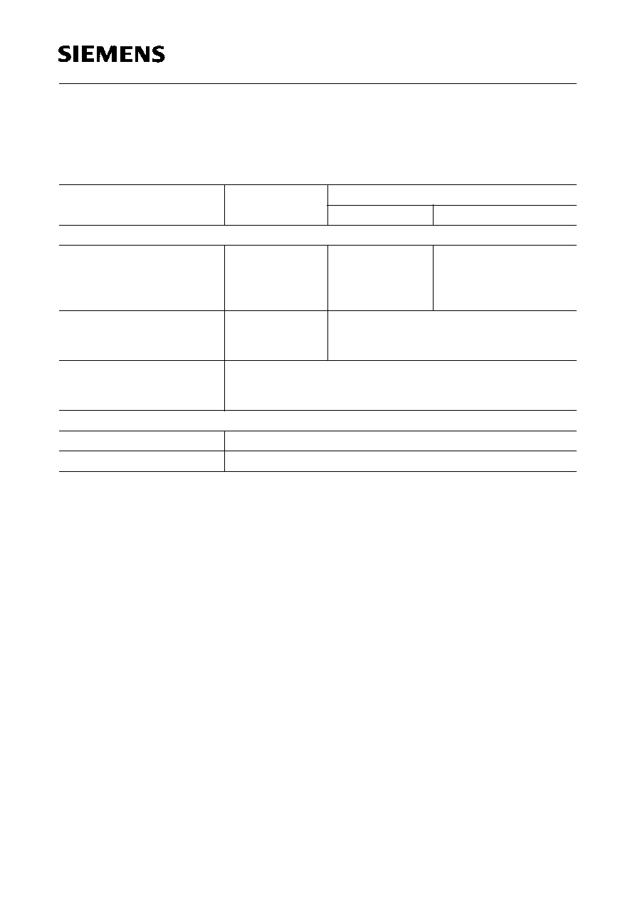
Chip Address
There are two pairs of chip addresses, which are selected by the CS0-input pin according to the
following table
Write Mode
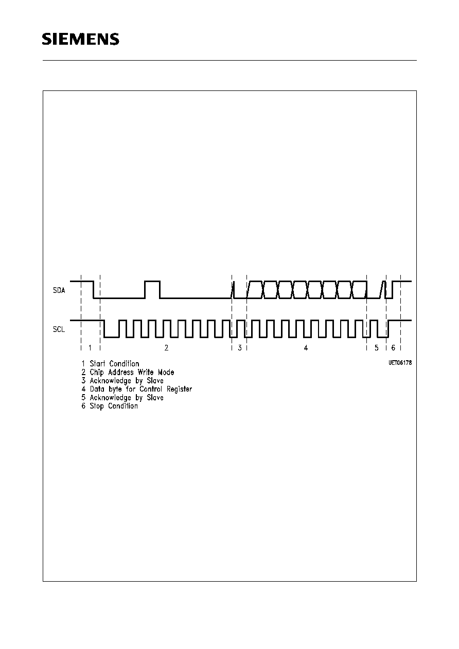
For writing to the PDC decoder, the following format has to be used:
Data Transfer (Write Mode)
Step1
: In order to start a data transfer the master generates a Start Condition on the bus by pulling
the SDA line low while the SCL line is held high.
Step 2
: The bus master puts the chip address on the SDA line during the next eight SCL pulses.
Step 3
: The master releases the SDA line during the ninth clock pulse. Thus the slave can generate
an acknowledge (AS) by pulling the SDA line to a low level.
Step 4
: The controller transmits the data byte to set the Control register.
Step 5
: The slave acknowledges the reception of the byte.
Step 6
: The master concludes the data communication by generating a Stop Condition.
The write mode is used to set the
I
2
C-Bus control register which determines the operating mode:
CS0 Input
Write Mode
Read Mode
Low
20 (hex)
21 (hex)
High
22 (hex)
23 (hex)
START
Chipadress White Mode
AS
Byte Set Control Register
AS
STOP
SDA 5648
SDA 5648X
Semiconductor Group
27
Control Register
Default: All bits are set to 0 on power-up.
Bit 0:
Determines, which kind of data is accessed via the
I
2
C-Bus when PDC mode is active.
Bit 1:
Determines the operating mode.
Bits 2 through 7 are used for test purposes.
DIS: Don`t care.
Bits 3 through 7 must not be changed for normal operation by user software!
Read Mode
For reading from the PDC decoder, the following format has to be used.
Bit Number
7
6
5
4
3
2
1
0
T4
T3
T2
T1
T0
DIS
PDC/
VPS
FOR1/
FOR2
Value
0
1
BDSP
8/ 30/ 2
data accessible
BDSP 8/ 30/ 1 or
header row
data accessible (refer to description of Bit 2)
Value
0
1
VPS mode active
PDC mode active
START
Chipaddress Read Mode
AS
1st Byte
AM
...
Last
Byte
NAM
STOP

SDA 5648
SDA 5648X
Semiconductor Group
28
Data Transfer (Read Mode)
Step1
: To start a data transfer the master generates a Start Condition on the bus by pulling the
SDA line low while the SCL line is held high. The byte address counter in the decoder is
reset and points to the first byte to be output.
Step 2
: The bus master puts the chip address on the SDA line during the next eight SCL pulses.
Step 3
: The master releases the SDA line during the ninth clock pulse. Thus the slave can generate
an acknowledge (AS) by pulling the SDA line to a low level. At this moment, the slave
switches to transmitting mode.
Step 4
: During the next eight clock pulses the slave puts the addressed data byte onto the SDA
line.
Step 5
: The reception of the byte is acknowledged by the master device which, in turn, pulls down
the SDA line during the next SCL clock pulse. By acknowledging a byte, the master
prompts the slave to increment its internal address counter and to provide the output of the
next data byte.
Step 6
: Steps no. 4 and no. 5 are repeated, until the desired amount of bytes have been read.
Step 7
: The last byte is output by the slave since it will not be acknowledged by the master.
Step 8
: To conclude the read operation, the master doesn't acknowledge the last byte to be
received. A No Acknowledge by the master (NAM) causes the slave to switch from
transmitting to receiving mode. Note that the master can prematurely cease any reading
operation by not acknowledging a byte.
Step 9
: The master gains control over the SDA line and concludes the data transfer by generating
a Stop Condition on the bus, i. e., by producing a low/high transition on the SDA line while
the SCL line is in a high state. With the SDA and the SCL lines being both in a high state,
the
I
2
C-Bus is free and ready for another data transfer to be started.
The contents of up to 7 registers (bytes) can be read starting with byte 1 bit 7 (refer to the following
table).
SDA 5648
SDA 5648X
Semiconductor Group
29
Order of Data Output on the
I
2
C-Bus and Bit Allocation of the 3 Different Operating Modes
I
2
C-Bus
PDC Packet 8/30
VPS Mode
Format 1
Format 2
Byte 1
bit 7
6
5
4
3
2
1
0
byte 15
bit 0
2)
1
2
3
4
5
6
7
byte 16
bit 0
1)
1
2
3
byte 17
bit 0
1
2
3
byte 11
bit 0
2)
1
2
3
4
5
6
7
Byte 2
bit 7
6
5
4
3
2
1
0
byte 16
bit 0
1
2
3
4
5
6
7
byte 18
bit 0
1
2
3
byte 19
bit 0
1
2
3
byte 12
bit 0
1
2
3
4
5
6
7
Byte 3
bit 7
6
5
4
3
2
1
0
byte 17
bit 0
1
2
3
4
5
6
7
byte 20
bit 0
1
2
3
byte 21
bit 0
1
2
3
byte 13
bit 0
1
2
3
4
5
6
7
Byte 4
bit 7
6
5
4
3
2
1
0
byte 18
bit 0
1
2
3
4
5
6
7
byte 22
bit 0
1
2
3
byte 23
bit 0
1
2
3
byte 14
bit 0
1
2
3
4
5
6
7
t
1) Message bit numbers according to EBU specification of PDC system.
2) Transmission bit number
SDA 5648
SDA 5648X
Semiconductor Group
30
Order of Data Output on the
I
2
C-Bus and Bit Allocation of the 3 Different Operating Modes
(cont'd)
I
2
C-Bus
PDC Packet 8/30
VPS Mode
Format 1
Format 2
Byte 5
bit 7
6
5
4
3
2
1
0
byte 19
bit 0
1
2
3
4
5
6
7
byte 14
bit 0
1
2
3
byte 15
bit 0
1
2
3
byte 5
bit 0
1
2
3
4
5
6
7
Byte 6
bit 7
6
5
4
3
2
1
0
byte 20
bit 0
1
2
3
4
5
6
7
byte 24
bit 0
1
2
3
byte 25
bit 0
1
2
3
byte 15
bit 0
1
2
3
4
5
6
7
Byte 7
bit 7
6
5
4
3
2
1
0
byte 21
bit 0
1
2
3
4
5
6
7
byte 13
bit 0
1
2
3
≠ set to "1"
≠ set to "1"
≠ set to "1"
≠ set to "1"
≠ set to "1"
≠ set to "1"
≠ set to "1"
≠ set to "1"
≠ set to "1"
≠ set to "1"
≠ set to "1"
≠ set to "1"
SDA 5648
SDA 5648X
Semiconductor Group
31
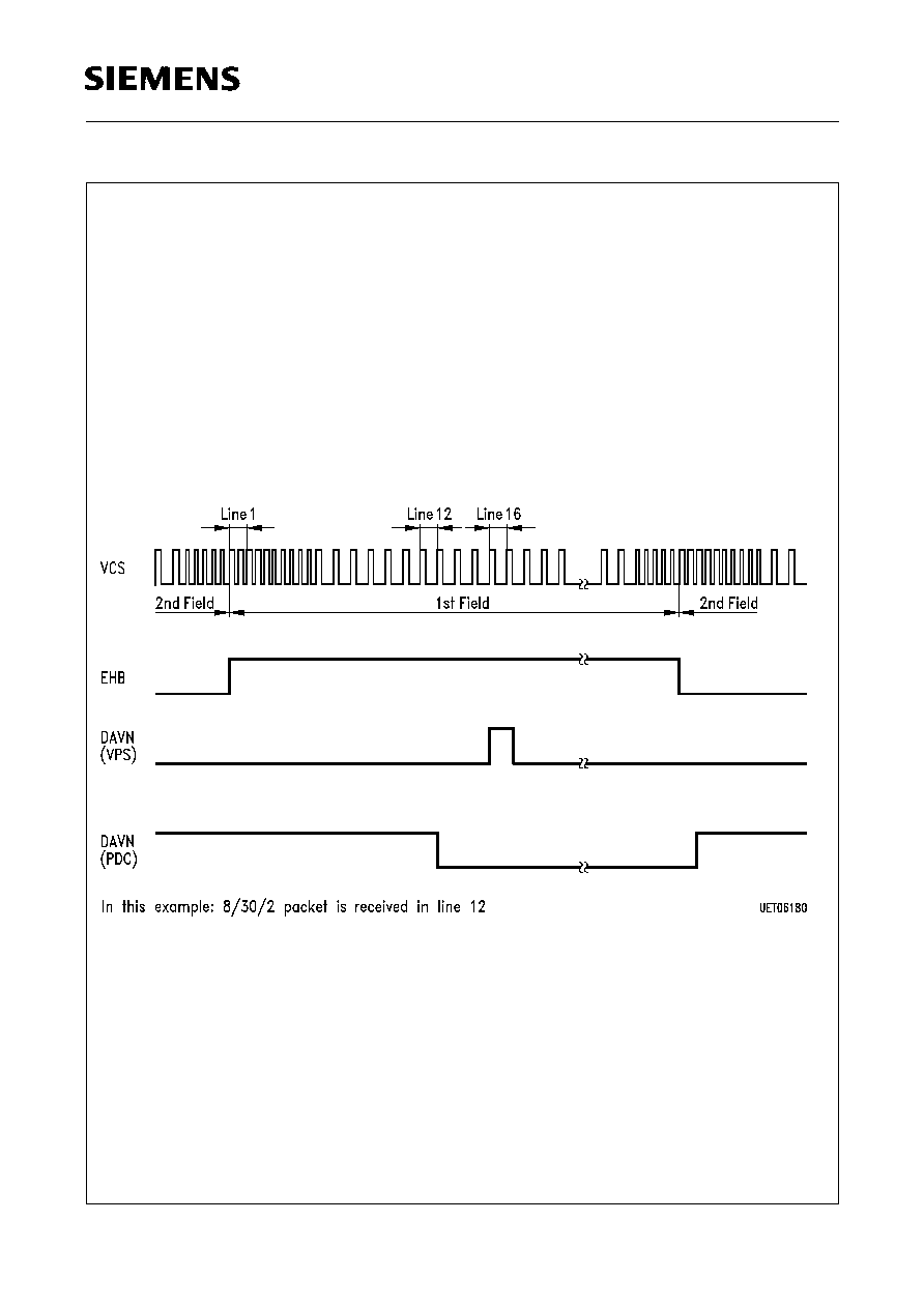
Description of DAVN and EHB Outputs
DAVN (Data Valid active low)
EHB (First Field active high)
In test mode (i.e. TI = high), both DAVN and EHB are controlled by the CS0 pin and reproduce the
state of the CS0 input.
Signal Output
VPS Mode
PDC Mode
8/30/2
8/30/1
DAVN
H/L-transition
(set low)
in line 16 when
valid VPS data is
received
in the line
carrying
valid
8/30/2 data
in the line
carrying
valid
8/30/1 data
L/H-transition
(set high)
at the start of
line 16
at the beginning of the next field
i.e.,at the start of the next data entry window
always set high
on power-up or
during
I
2
C-Bus accesses when the bus master doesn't
acknowledge in order to generate the stop condition
EHB
L/H-transition
at the beginning of the first field
H/L-transition
at the beginning of the second field
SDA 5648
SDA 5648X
Semiconductor Group
32
Electrical Characteristics
Absolute Maximum Ratings
T
A
= 25
∞
C
Parameter
Symbol
Limit Values
Unit
Test
Condition
min.
typ.
max.
Ambient temperature
T
A
0
70
∞
C
in operation
Storage temperature
T
stg
≠ 40
125
∞
C
by storage
Total power dissipation
P
tot
300
mW
Power dissipation per output
P
DQ
10
mW
Input voltage
V
IM
≠ 0.3
6
V
Supply voltage
V
DD
≠ 0.3
6
V
Thermal resistance
R
th SU
80
K/W
Operating Range
Supply voltage
V
DD
4.5
5
5.5
V
Supply current
I
DD
5
15
mA
Ambient temperature range
T
A
0
70
∞
C
Characteristics
T
A
= 25
∞
C
Parameter
Symbol
Limit Values
Unit
Test
Condition
min.
typ.
max.
Input Signals SDA, SCL, CS0
H-input voltage
V
IH
0.7
◊
V
DD
V
DD
V
L-input voltage
V
IL
0
0.3
◊
V
DD
V
Input capacitance
C
I
10
pF
Input current
I
IM
10
µ
A
Input Signal TI
H-input voltage
V
IH
0.9
◊
V
DD
V
DD
V
L-input voltage
V
IL
0
0.1
◊
V
DD
V
Input capacitance
C
I
10
pF
Input current
I
IM
10
µ
A
SDA 5648
SDA 5648X
Semiconductor Group
33
Input Signals CVBS
(pos. Video, neg. Sync)
Video input signal level
V
CVBS
0.7
1.0
2.0
V
Synchron signal amplitude
V
SYNC
0.15
0.3
1.0
V
Data amplitude
V
DAT
0.25
1.5
◊
V
SYNC
0.5
1.0
V
VPS mode
PDC mode
Coupling capacitor
C
C
33
nF
H-input current
I
IH
10
µ
A
V
I
= 5 V
L-input current
I
IL
≠ 1000
≠ 400
≠ 100
µ
A
V
I
= 0 V
Source impedance
R
S
250
Leakage resistance at
coupling capacitor
R
C
0.91
1
1.2
M
Output Signals DAVN, EHB, VCS
H-output voltage
V
QH
V
DD
≠ 0.5
V
I
Q
= ≠ 100
µ
A
L-output voltage
V
QL
0.4
V
I
Q
= 1.6 mA
Output Signals SDA (Open-Drain-Stage)
L-output voltage
V
QL
0.4
V
I
Q
= 3.0 mA
Permissible output voltage
5.5
V
PLL-Loop Filter Components (see application circuit)
Resistance at PD2/VCO2
R
1
6.8
k
Resistance at VCO1
R
2
1200
k
Attenuation resistance
R
3
6.8
k
Resistance at PD2/VCO2
R
5
1200
k
Integration capacitor
C
1
2.2
nF
Integration capacitor
C
3
33
nF
VCO ≠ Frequence Range Adjustment
Resistance at IREF (for bias
current adjustment)
R
4
100
k
Characteristics (cont'd)
T
A
= 25
∞
C
Parameter
Symbol
Limit Values
Unit
Test
Condition
min.
typ.
max.
SDA 5648
SDA 5648X
Semiconductor Group
34
I
2
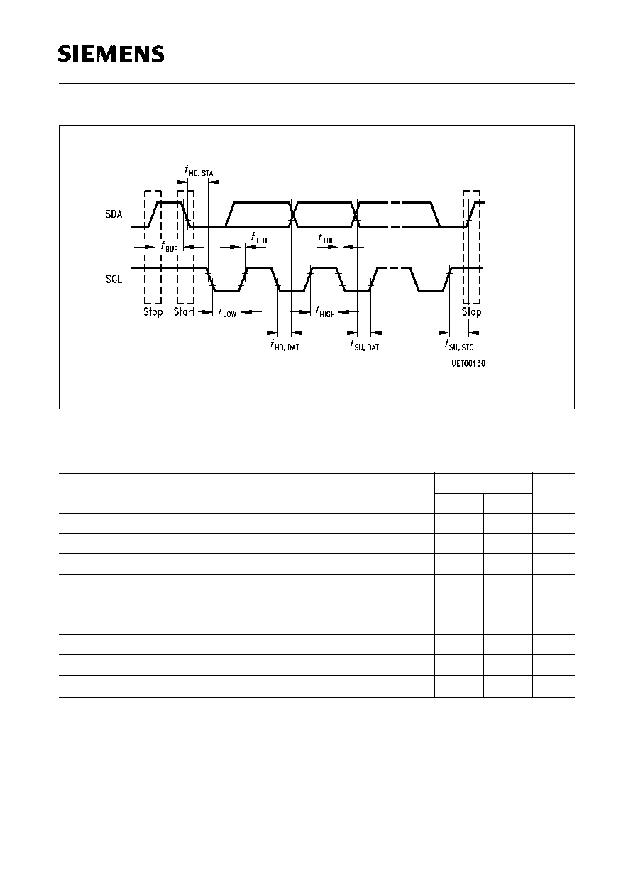
C-Bus Timing
All values referred to
V
IH
and
V
IL
levels.
Parameter
Symbol
Limit Values
Unit
min.
max.
Clock frequency
f
SCL
0
100
kHz
Inactive time prior to new transmission start-up
t
BUF
4.7
µ
s
Hold time during start condition
t
HD;STA
4.0
µ
s
Low-period of clock
t
LOW
4.7
µ
s
High-period of clock
t
HIGH
4.0
µ
s
Set-up time for data
t
SU;DAT
250
ns
Rise time for SDA and SCL signal
t
TLH
1
µ
s
Fall time for SDA and SCL signal
t
THL
300
ns
Set-up time for SCL clock during stop condition
t
SU;STO
4.7
µ
s
SDA 5648
SDA 5648X
Semiconductor Group
35
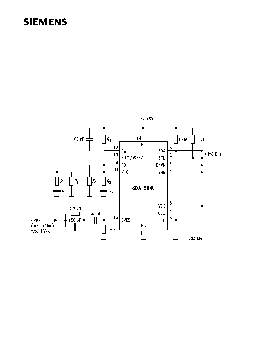
PDC/VPS-Receiver
Application Circuit
SDA 5648
SDA 5648X
Semiconductor Group
36
I
2
C-Bus Signals During Write Operations
SDA 5648
SDA 5648X
Semiconductor Group
37
I
2
C-Bus Signals During Read Operations
SDA 5648
SDA 5648X
Semiconductor Group
38
SDA 5648
SDA 5648X
Semiconductor Group
39
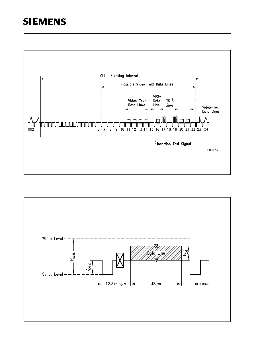
Position of Teletext and VPS Data Lines within the Vertical Blanking Interval
(shown for first field)
Definition of Voltage Levels for VPS Data Line
SDA 5648
SDA 5648X
Semiconductor Group
40
BDSP 8/30 Format 1 Bit Allocation
This corresponds to the coding adopted in CCIR teletext system B BDSP 8/30 format 1.
NB: The received bytes are output on the
I
2
C-bus in a transparent way, i.e., on a bit-first-in-first-out
basis. No bit manipulation is performed on the chip in this operating mode. When evaluating the
numbers, note that each 4-bit-digit has been incremented by one prior to transmission, and the least
significant bits are transmitted first.
Byte No.
Bit No.
Contents
0
1
2
3
4
5
6
7
Time Offset Code
15
Weight
Weight
Sign
2
≠ 2
2
≠ 1
2
0
2
1
2
2
2
3
0
1
16
MJD Digit
Weight 10
4
1
1
1
1
Modified Julian Date (MJD)
1. Byte
17
MJD Digit
Weight 10
2
MJD Digit
Weight 10
3
Modified Julian Date
2. Byte
18
MJD Digit
Weight 10
0
MJD Digit
Weight 10
1
Modified Julian Date (MJD)
3. Byte
19
UTC Hours
Units
UTC Hours
Tens
Universal Time Coordinated (UTC)
1. Byte
20
UTC Minutes
Units
UTC Minutes
Tens
Universal Time Coordinated
2. Byte
21
UTC Seconds
Units
UTC Seconds
Tens
Universal Time Coordinated
3. Byte
SDA 5648
SDA 5648X
Semiconductor Group
41
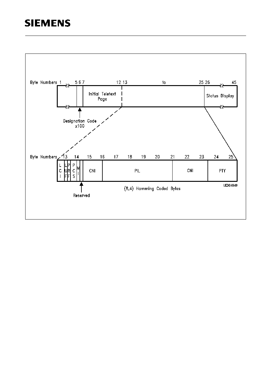
Structure of the Teletext Data Packet 8/30 Format 2

SDA 5648
SDA 5648X
Semiconductor Group
42
BDSP 8/30 Format 2 Bit Allocation
The four message bits of byte 13 are used as follows:
byte 13 bit 0 ≠ LCI b
1
)
label channel identifier
1 ≠ LCI b
2
)
2 ≠ LUF
label update flag
3 ≠ reserved but as yet undefined
The message bits of bytes 14 ≠ 25 are used in a way similar to the coding of the label in the
dedicated television line as follows:
byte 14 bit 0 PCS b
1
)
status of
byte 20 bit 0 PIL
b
15
)
1 PCS b
2
)
analogue sound
1 PIL
b
16
)
2 PIL
b
17
)
minute
2
)
reserved but yet
3 PIL
b
18
)
3
)
undefined
byte 21 bit 0 PIL
b
19
)
1 PIL
b
20
)
byte 15 bit 0 CNI
b
1
)
1 CNI
b
2
)
country
2 CNI
b
5
)
2 CNI
b
3
)
3 CNI
b
6
)
country
3 CNI
b
4
)
byte 22 bit 0 CNI
b
7
)
1 CNI
b
8
)
byte 16 bit 0 CNI
b
9
)
network (or
1 CNI
b
10
)
program provider)
2 CNI
b
11
)
3 CNI
b
12
)
2 PIL
b
1
)
byte 23 bit 0 CNI
b
13
)
network (or
3 PIL
b
2
)
1 CNI
b
14
)
program
byte 17 bit 0 PIL
b
3
)
day
2 CNI
b
15
)
provider)
1 PIL
b
4
)
3 CNI
b
16
)
2 PIL
b
5
)
byte 24 bit 0 PTY b
1
)
3 PIL
b
6
)
1 PTY b
2
)
byte 18 bit 0 PIL
b
7
)
month
2 PTY b
3
)
1 PIL
b
8
)
3 PTY b
4
)
program
2 PIL
b
9
)
byte 25 bit 0 PTY b
5
)
type
1 PTY b
6
)
3 PIL
b
10
)
2 PTY b
7
)
byte 19 bit 0 PIL
b
11
)
3 PTY b
8
)
1 PIL
b
12
)
hour
2 PIL
b
13
)
3 PIL
b
14
)
SDA 5648
SDA 5648X
Semiconductor Group
43
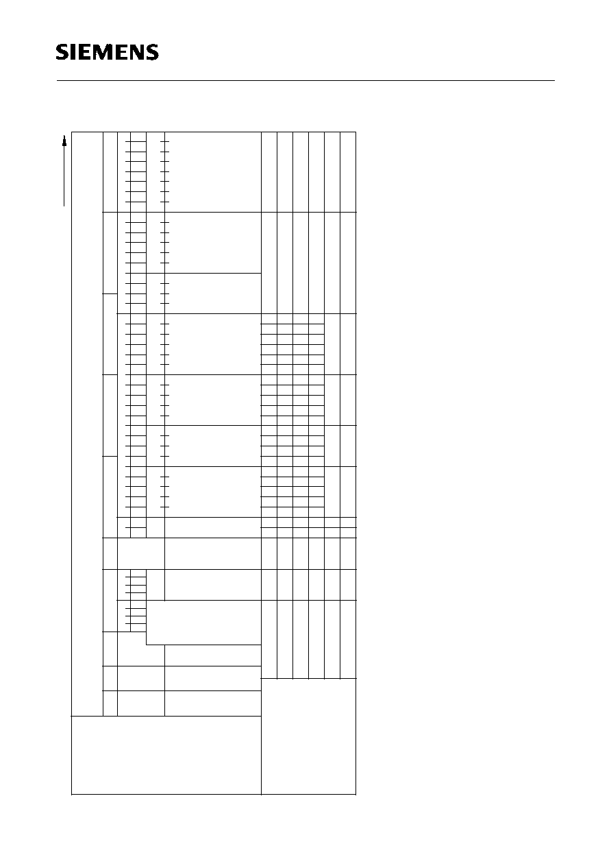
Data Format of the Program Delivery Data in the Dedicated TV Line
Time
Parameter
PCS
CNI
CNI
PIL
CNI
PTY
Byte No.
1
2
3 & 4
5
6 to 10
11
12
13
14
15
Parameter bits b
i
, I =
12341234
9
1
0
1
2
3
4
5
6
7
8
9
1
0
1
1
1
2
1
3
1
4
1
5
1
6
1
7
1
8
1
9
2
0
5
6
7
8
1
1
1
2
1
3
1
4
1
5
1
6
1
2
3
4
5
6
7
8
Transmission bit No.
01234567
0
1
2
3
4
5
6
7
0
1
2
3
4
5
6
7
0
1
2
3
4
5
6
7
0
1
2
3
4
5
6
7
0
1
2
3
4
5
6
7
Bits b
1
and
b
2
: 00 don't
know
01
mono
10
stereo
11
dual
sound
Bits b
3
and
b
4
are
reserved
M
L
ML
M
L
ML
M
L
M
L
M
L
M
L
Content
Clock
run-in
Start
code
Not relevant
to PDC
Reserved for
enhancement
of VPS
Not relevant
to PDC
Net.
or
prog.
prov.
bin.
Day
binary
Month
binary
Hour
binary
Minute
binary
Country
binary
Network or
program
provider
binary
Program type
binary
Reserved code
values for
receiver control
(service codes)
Timer control code
N
.......
N
N
N
0
0
0
0
0
1
1
1
1
1
1
1
1
1
1
1
1
1
1
1
N
.......................................
N
A
.............................
A
Record inhibit/term.
N
.......
N
N
N
0
0
0
0
0
1
1
1
1
1
1
1
1
0
1
1
1
1
1
1
N
.......................................
N
A
.............................
A
Interruption code
N
.......
N
N
N
0
0
0
0
0
1
1
1
1
1
1
1
0
1
1
1
1
1
1
1
N
.......................................
N
A
.............................
A
Continuation code
N
.......
N
N
N
0
0
0
0
0
1
1
1
1
1
1
1
0
0
1
1
1
1
1
1
N
.......................................
N
A
.............................
A
Unenhanced VPS
1111
N
N
P
...................
................
......................
......................
P
N
.......................................
N
A
.............................
A
PTY not in use
N
.......
N
N
N
P
...................
................
......................
......................
P
N
.......................................
N
1
1
1
1
1
1
1
1
Abbreviations:
CNI
=
Country and Network Identification
PCS
=
Program Control Status
PIL
=
Program Identification Label
PTY
=
Program Type
M
=
Most-significant bit
L
=
Least-significant bit
A
=
Bit value is that of the current PTY code
N
=
Bit value is that of the current CNI code
P
=
Bit value is that of the current PIL code
......
......
......
......
......
.......
.......