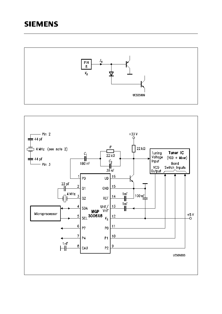
Combined with a VCO (tuner), the MGP 3006X6 device, with four hard-switched chip
addresses, forms a digitally programmable phase-locked loop for use in television sets
with PLL-frequency synthesis tuning. The PLL permits precise crystal-controlled setting
of the frequency of the tuner oscillator between 16 and 1300 MHz in increments of
62.5 kHz, and, with a 2.4-GHz prescaler 1/2, in the TV-SAT band in increments of
125 kHz. The tuning process is controlled by a microprocessor via an
I
2
C Bus. The
I
2
C Bus noise immunity has been improved by a factor of 10 compared to the
SDA 3202-2, and the new crystal oscillator generates a sinusoidal signal, suppressing
the higher-order harmonics, which reduces the moirÈ noise considerably.
Type
Ordering Code
Package
MGP 3006X6
Q67000-H5113
P-DSO-16-1 (SMD)
MGP 3006X6
Q67006-H5113
P-DSO-16-1 Tape & Reel (SMD)
GHz PLL with
I
2
C Bus
and Four Chip Addresses
Bipolar IC
MGP 3006X6
P-DSO-16-1
Features
q
1-chip system for MPU-control (
I
2
C Bus)
q
4 programmable chip addresses
q
Short pull-in time for quick channel switch-over
and optimized loop stability
q
3 high-current band switch outputs (20 mA)
q
Software-compatible with SDA 3202 series
q
Oxis III technology
Semiconductor Group
1
04.93

Semiconductor Group
2
MGP 3006X6
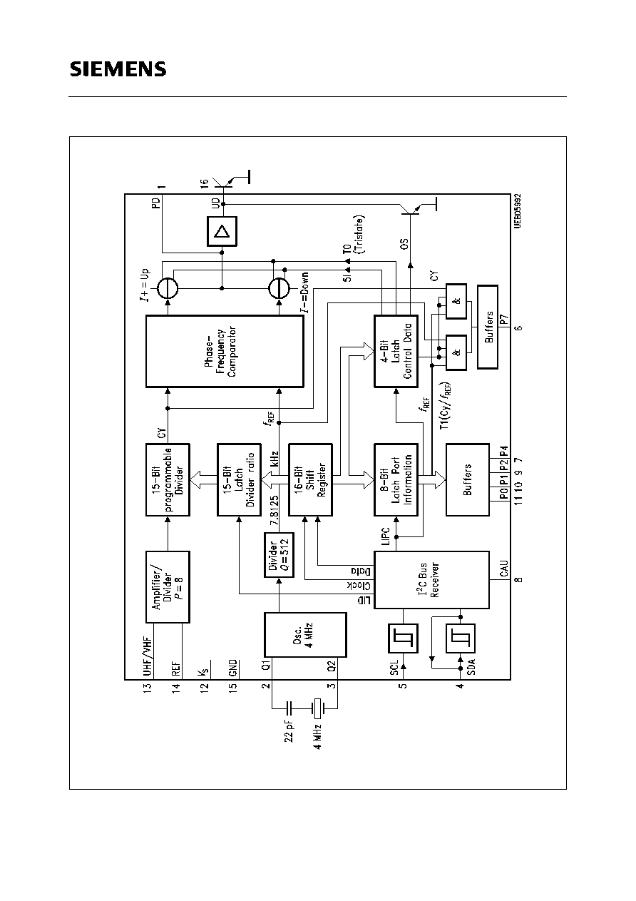
Circuit Description
Tuning Section
UHF/VHF
The tuner signal is capacitively coupled at the UHF/VHF-input and
subsequently amplified.
REF
The reference input REF should be decoupled to ground using a capacitor
of low series inductance. The signal passes through an asynchronous
divider with a fixed ratio of
P
= 8, an adjustable divider with ratio
N
= 256
through 32767, and is then compared in a digital frequency/phase
detector to a reference frequency
f
REF
= 7.8125 kHz.
Q1, Q2
This frequency is derived from a balanced, low-impedance 4-MHz crystal
oscillator (pin Q1, Q2) by dividing its output signal by
Q
= 512.
The phase detector has two outputs UP and DOWN that drive the two
current sources I+ and I≠ of a charge pump. If the negative edge of the
divided VCO-signal appears prior to the negative edge of the reference
signal, the I+ current source pulses for the duration of the phase
difference. In the reverse case the I≠ current source pulses.
PD, UD
If the two signals are in phase, the charge pump output (PD) goes into the
high-impedance state (PLL is locked). An active low-pass filter integrates
the current pulses to generate the tuning voltage for the VCO (internal
amplifier, external output transistor at UD and external RC-circuitry). The
charge pump output is also switched into the high-impedance state when
the control bit T0 = 1. Here it should be noted, however, that the tuning
voltage can alter over a long period in the high-impedance state as a
result of self-discharge in the peripheral circuitry. UD may be switched off
by the control bit OS to allow external adjustments.
By means of a control bit 5I the pump current can be switched between
two values by software. This programmability permits alteration of the
control response of the PLL in the locked-in state. In this way different
VCO-gains in the different TV-bands can be compensated, for example.
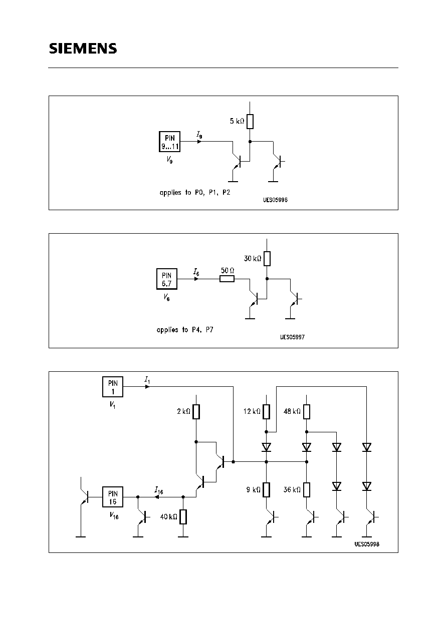
P0, P1, P2
The software-switched outputs P0, P1, P2 can be used for direct band
selection (20 mA current output).
P4, P7
P4 and P7 are general-purpose open-collector outputs. The test bit T1 = 1
switches the test signal Cy (divided input signal) to P7.
CAU
Four different chip addresses can be set by appropriate connection of pin
CAU.

MGP 3006X6
Semiconductor Group
3
I
2
C Bus Interface
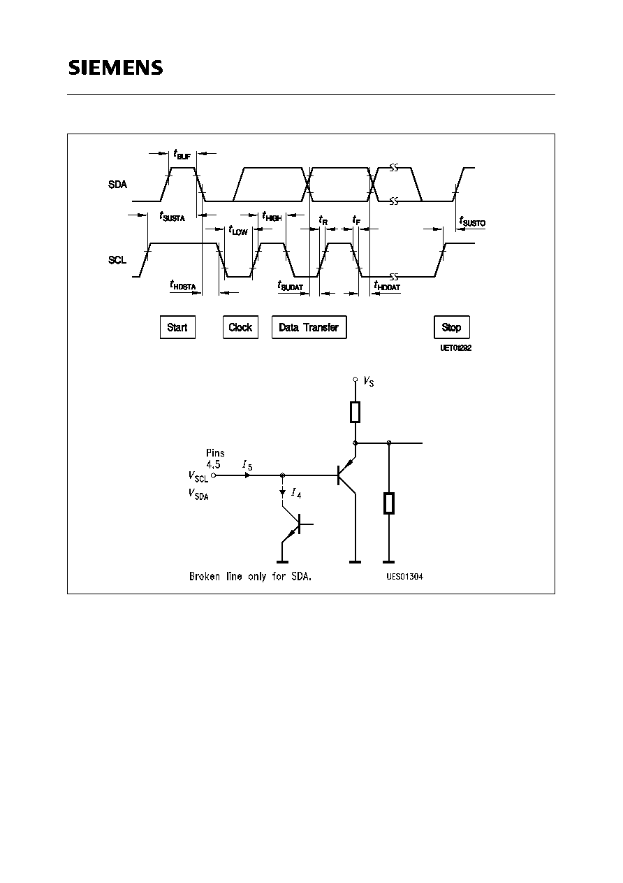
Data are exchanged between the processor and the PLL on the
I
2
C Bus.
SCL, SDA
The clock is generated by the processor (input SCL), while pin SDA works
as an input or output depending on the direction of the data (open
collector; external pull-up resistor). Both inputs have hysteresis and a
low-pass characteristic, which enhances the noise immunity of the
I
2
C
Bus.
The data from the processor pass through an
I
2
C Bus control. Depending
on their function the data are subsequently stored in registers. If the bus
is free, both lines will be in the marking state (SDA, SCL are high). Each
telegram begins with the start condition and ends with the stop condition.
Start condition: SDA goes low, while SCL remains high. Stop condition:
SDA goes high while SCL remains high. All further information transfer
takes place during SCL = low, and the data is forwarded to the control
logic on the positive clock edge.
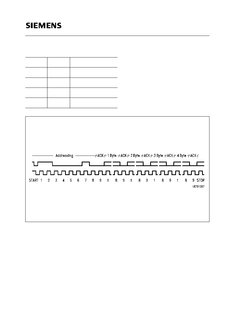
The table "bit allocation" should be referred to in the following paragraph.
All telegrams are transmitted byte-by-byte, followed by a ninth clock
pulse, during which the control logic returns the SDA-line to low
(acknowledge condition). The first byte is comprised of seven address
bits. These are used by the processor to select the PLL from several
peripheral components (chip select). The eighth bit is always low.
In the data portion of the telegram the first bit of the first or third data byte
determines whether a divider ratio or control information is to follow. In
each case the second byte of the same data type or a stop condition has
to follow the first byte.
V
S
, GND
When the supply voltage is applied a power-on reset circuit prevents the
PLL from setting the SDA-line to low, which would block the bus.
Semiconductor Group
4
MGP 3006X6
Circuit Description (cont'd)
Bit Allocation
Divider Ratio
N = 16384
◊
n14 + 8192
◊
n13 + 4096
◊
n12 + 2048
◊
n11 + 1024
◊
n10 + 512
◊
n9 +
256
◊
n8 + 128
◊
n7 + 64
◊
n6 + 32
◊
n5 + 16
◊
n4 + 8
◊
n3 + 4
◊
n2 + 2
◊
n1 + n0
Band Selection
P0, P1, P2, P4, P7 = 1
Open-collector output is active.
Pump Current Programming
5I = 1
High current
UD Disable
OS = 1
UD is disabled.
Test Mode
T1, T0 = 0, 0
Normal operation
T1 = 1
P3 =
f
REF
; P4 = Cy
T0 = 1
Tristate: charge pump output PD is in high-impedance state.
MSB
A = Acknowledge
Address byte
1
1
0
0
0
MA1
MA0
0
A
Prog. divider Byte 1
0
n14
n13
n12
n11
n10
n9
n8
A
Prog. divider Byte 2
n7
n6
n5
n4
n3
n2
n1
n0
A
Control info. Byte 1
1
5I
T1
T0
X
X
1
OS
A
Control info. Byte 2
P7
X
X
P4
X
P2
P1
P0
A
MGP 3006X6
Semiconductor Group
5
Chip Address Switching
Telegram Examples
Start-Addr-DR1-DR2-CW1-CW2-Stop
Start
=
start condition
Start-Addr-CW1-CW2-DR1-DR2-Stop
Addr
=
address
Start-Addr-DR1-DR2-CW1-Stop
DR1
=
divider ratio 1st byte
Start-Addr-CW1-CW2-DR1-Stop
DR2
=
divider ratio 2nd byte
Start-Addr-DR1-DR2-Stop
CW1
=
control word 1st byte
Start-Addr-CW1-CW2-Stop
CW2
=
control word 2nd byte
Start-Addr-DR1-Stop
Stop
=
stop condition
Start-Addr-CW1-Stop
MA1
MA0
Voltage at CAU
0
0
(0 ... 0.1)
V
S
0
1
open-circuit
1
0
(0.4 ... 0.6)
V
S
1
1
(0.9 ... 1)
V
S
Semiconductor Group
6
MGP 3006X6
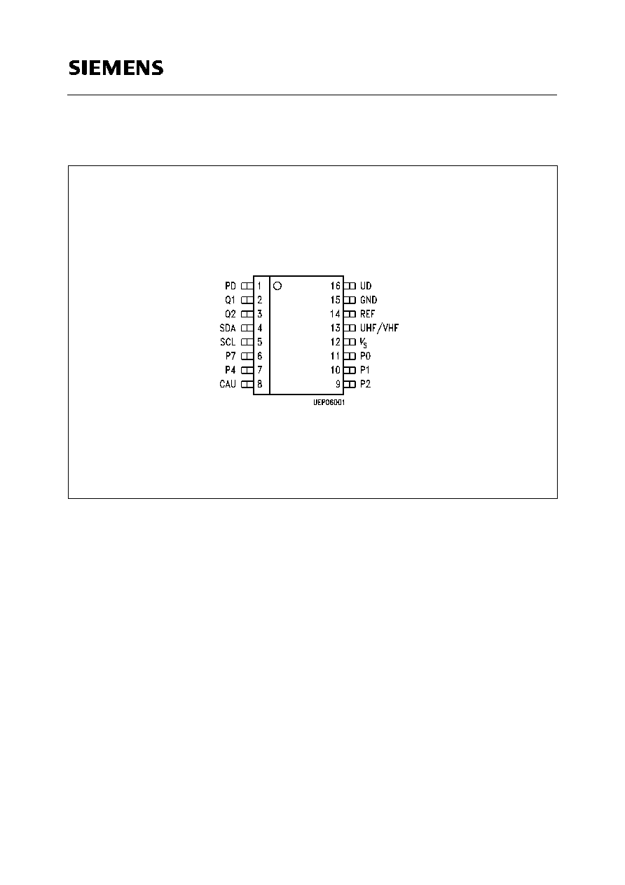
Pin Configuration
(top view)
MGP 3006X6
Semiconductor Group
7
Pin Definitions and Functions
Pin No.
Symbol
Function
1
PD
Input active filter/charge pump output
2
Q1
Quartz crystal
3
Q2
Quartz crystal
4
SDA
Data input/output for
I
2
C Bus
5
SCL
Clock input for
I
2
C Bus
6
P7
Port output (open collector)
7
P4
Port output (open collector)
8
CAU
Address switch input
9
P2
Port output (open collector)
10
P1
Port output (open collector)
11
P0
Port output (open collector)
12
V
S
Supply voltage
13
UHF/VHF
Signal input
14
REF
Amplifier reference input
15
GND
Ground
16
UD
Output active filter
Semiconductor Group
8
MGP 3006X6
Block Diagram
MGP 3006X6
Semiconductor Group
9
Absolute Maximum Ratings
T
A
= ≠ 20 to 80
∞
C
Parameter
Symbol
Limit Values
Unit
Remarks
min.
max.
Supply voltage
V
S
≠ 0.3
6
V
Output PD
V
1
≠ 0.3
V
S
V
Crystal oscillator pins Q1, Q2
V
2
≠ 0.3
V
S
V
Bus input/output SDA
V
4
≠ 0.3
6
V
Bus input SCL
V
5
≠ 0.3
6
V
Port outputs P0, P1, P2, P4, P7
V
6
≠ 0.3
16
V
Chip address switch CAU
V
8
≠ 0.3
V
S
V
Signal input UHF/VHF
V
13
≠ 0.3
0.3
V
for
V
S
= 0 V
Reference input REF
V
14
≠ 0.3
0.3
V
for
V
S
= 0 V
Output active filter UD
V
16
≠ 0.3
V
S
V
Bus output SDA
I
4L
≠ 1
5
mA
open collector
Port outputs P0, P1, P2
I
9L
≠ 1
20
mA
open collector
Port outputs P4
P7
I
7L
I
6L
≠ 1
≠ 1
5
7
mA
mA
open collector
open collector
Total port output current
I
L
25
mA
Junction temperature
T
j
125
∞
C
Storage temperature
T
stg
≠ 40
125
∞
C
Thermal resistance
(junction to ambient)
R
th JA
125
K/W
Semiconductor Group
10
MGP 3006X6
Operating Range
Supply voltage
V
S
4.5
5.5
V
Ambient temperature
T
A
≠ 20
80
∞
C
Input frequency
f
13
16
1300
MHz (at 25
∞
C)
Crystal frequency
f
2
3.2
4.8
MHz
Programmable divider factor
N
256
32767
AC/DC Characteristics
T
A
= ≠ 20 to 80
∞
C;
V
S
= 4.5 to 5.5 V
Parameter
Symbol
Limit Values
Unit
Test Condition
Test
Circuit
min.
typ.
max.
Supply current
I
S
41
55
mA
V
S
= 5 V
1
Crystal Oscillator Connections Q1, Q2
Oscillation frequency
f
2
3.99975
4.000
4.00025
MHz
f
Q
= 4 MHz
1
Margin from 1st
(fundamental) to 2nd
and 3rd harmonics
1)
20
dB
Signal Input UHF/VHF
Sensitivity
a
13
a
13
a
13
-- 27/10
-- 27/10
-- 20/22
3/315
3/315
3/315
dBm/
2)
dBm/
2)
dBm/
2)
f
13
= 70 ... 500 MHz
f
13
= 1000 MHz
f
13
= 1100 MHz
2
2
2
Port Outputs P0, P1, P2 (switch with open collector)
H-output current
I
9H
10
µ
A
V
6H
= 13.5 V
3
L-output voltage
V
9L
0.5
V
I
6L
= 20 mA
3
Notes see page 11.
Absolute Maximum Ratings (cont'd)
T
A
= ≠ 20 to 80
∞
C
Parameter
Symbol
Limit Values
Unit
Remarks
min.
max.
MGP 3006X6
Semiconductor Group
11
1) Design note only: no 100 % final inspection.
2) mVrms into 50
.
3) Ripple voltage on tuning line (see application circuit) = 128
µ
s (
I
1Z
+
I
16
/
2
)(
C
1
+
C
2
) / (
C
1
C
2
)
e.g. for
I
16
= 8
µ
A,
C
1
= 180 nF,
C
2
= 9 pF, worst-case ripple voltage = 61
µ
A.
Port Outputs P4, P7 (switch with open collector)
H-output current
I
6H
10
µ
A
V
6H
= 13.5 V
4
L-output voltage
V
6L
0.5
V
I
6L
= 1.7 mA
4
Phase-Detector Output PD (
V
S
= 5 V)
Pump current
Pump current
I
1H
I
1H
±
90
±
22
±
220
±
50
±
300
±
75
µ
A
µ
A
5I = 1;
V
1
= 2 V
5I = 0;
V
1
= 2 V
5
5
Tristate current
3)
I
1Z
≠ 3
1
3
nA
T1 = 1;
V
1
= 2 V
5
Current gain from
PD to UD
3)
2
6400
T1 = 1;
V
1
= 2 V;
I
1
= 2 nA
5
Output voltage
V
1L
1.0
2.5
V
locked
5
Active Filter Output UD (Test mode T0 = 1; PD = tristate)
Output current
≠
I
16
500
µ
A
V
16
= 0.8 V;
I
1H
= 90
µ
A
5
Output voltage
Output voltage
V
16
V
16
100
500
mV
mV
V
1L
= 0 V
OS = 1;
V
S
= 5 V;
T
A
= 25
∞
C
5
5
Chip Address Switch CAU
Input current
Input current
I
8H
≠
I
8L
50
50
µ
A
µ
A
V
8H
= 5 V
V
8L
= 5 V
7
7
AC/DC Characteristics (cont'd)
T
A
= ≠ 20 to 80
∞
C;
V
S
= 4.5 to 5.5 V
Parameter
Symbol
Limit Values
Unit
Test Condition
Test
Circuit
min.
typ.
max.
Semiconductor Group
12
MGP 3006X6
AC/DC Characteristics
T
A
= ≠ 20 to 80
∞
C;
V
S
= 4.5 to 5.5 V; refer to test circuit 6
Parameter
Symbol
Limit Values
Unit
Test Condition
min.
typ.
max.
Bus Inputs SCL, SDA
H-input voltage
V
4IH
3
5.5
V
L-input voltage
V
4IL
1.5
V
H-input current
I
4IH
10
µ
A
V
4IH
=
V
S
L-input current
≠
I
4IL
20
µ
A
V
4IL
= 0 V
Bus Output SDA (open collector)
H-output current
I
4OH
10
µ
A
V
4OH
= 5.5 V
L-output voltage
V
4OL
0.4
V
I
4OL
= 3 mA
Edges SCL, SDA
Rise time
t
R
1
µ
s
Fall time
t
F
0.3
µ
s
Shift Clock SCL
Frequency
f
5
0
100
kHz
H-pulse width
t
5HIGH
4
µ
s
L-pulse width
t
5LOW
4.7
µ
s
Start
Set-up time
t
SUSTA
4.7
µ
s
Hold time
t
HDSTA
4
µ
s
Notes see page 19
MGP 3006X6
Semiconductor Group
13
1) Design note only: no 100 % final inspection.
Stop
Set-up time
t
SUSTO
4.7
µ
s
Bus free
t
BUF
4.7
µ
s
Data Transfer
Set-up time
t
SUDAT
0.25
µ
s
Hold time
t
HDDAT
0
µ
s
Input hysteresis
SCL, SDA
1)
300
mV
Low-pass cutoff
frequency SCL,
SDA
1)
500
kHz
AC/DC Characteristics (cont'd)
T
A
= ≠ 20 to 80
∞
C;
V
S
= 4.5 to 5.5 V; refer to test circuit 6
Parameter
Symbol
Limit Values
Unit
Test Condition
min.
typ.
max.

Semiconductor Group
14
MGP 3006X6
Test Circuit 1
Crystal Oscillator
MGP 3006X6
Semiconductor Group
15
Test Circuit 2
Measurement of Input Sensitivity
Calibration of Signal Generator
Semiconductor Group
16
MGP 3006X6
Test Circuit 3
Test Circuit 4
Test Circuit 5
MGP 3006X6
Semiconductor Group
17
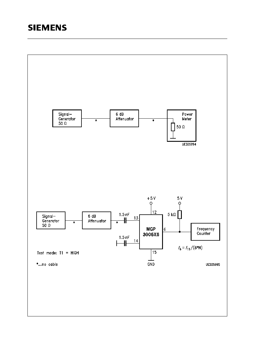
Test Circuit 6
I
2
C Bus Timing Diagram
Set-up time (start)
t
SUSTA
Hold time (start)
t
HDSTA
H-pulse width (clock)
t
HIGH
L-pulse width (clock)
t
LOW
Set-up time (data transfer)
t
SUDAT
Hold time (data transfer)
t
HDDAT
Set-up time (stop)
t
SUSTO
Bus free time
t
BUF
Fall time
t
F
Rise time
t
R
All times related to 10 % and 90 % values.
Semiconductor Group
18
MGP 3006X6
Test Circuit 7
Application Circuit

MGP 3006X6
Semiconductor Group
19
Notes
1. Loop bandwidth
R
=
[(
I
P
◊
K
VCO
) / (
C
1
◊
P
◊
N
)]
Attenuation
a
= 0.5
R
◊
R
◊
C
1
with
I
P
= charge pump current
K
VCO
= VCO-gain
R
,
C
1
= loop filter component values
P
= prescaler division ratio
N
= programmable division ratio
e.g.
I
P
= 50
µ
A,
K
VCO
= 18.7 MHz/V,
R
= 22 k
,
C
1
= 180 nF,
P
= 8,
N
= 11520 (channel 47):
R
= 237 Hz,
f
R
= 38 Hz,
a
= 0.47
Typically,
C
2
=
C
1
/5.
2. Symmetrical capacitive coupling improves the balance of the crystal oscillator and
thus reduces cross-talk.
3. High-impedance port outputs and the address selection input P3 can be decoupled
from external noise with a 1 nF capacitor.
4. It is important to keep to the
I
2
C Bus specification concerning maximum capacitance
and impedance.
Semiconductor Group
20
MGP 3006X6
Diagrams
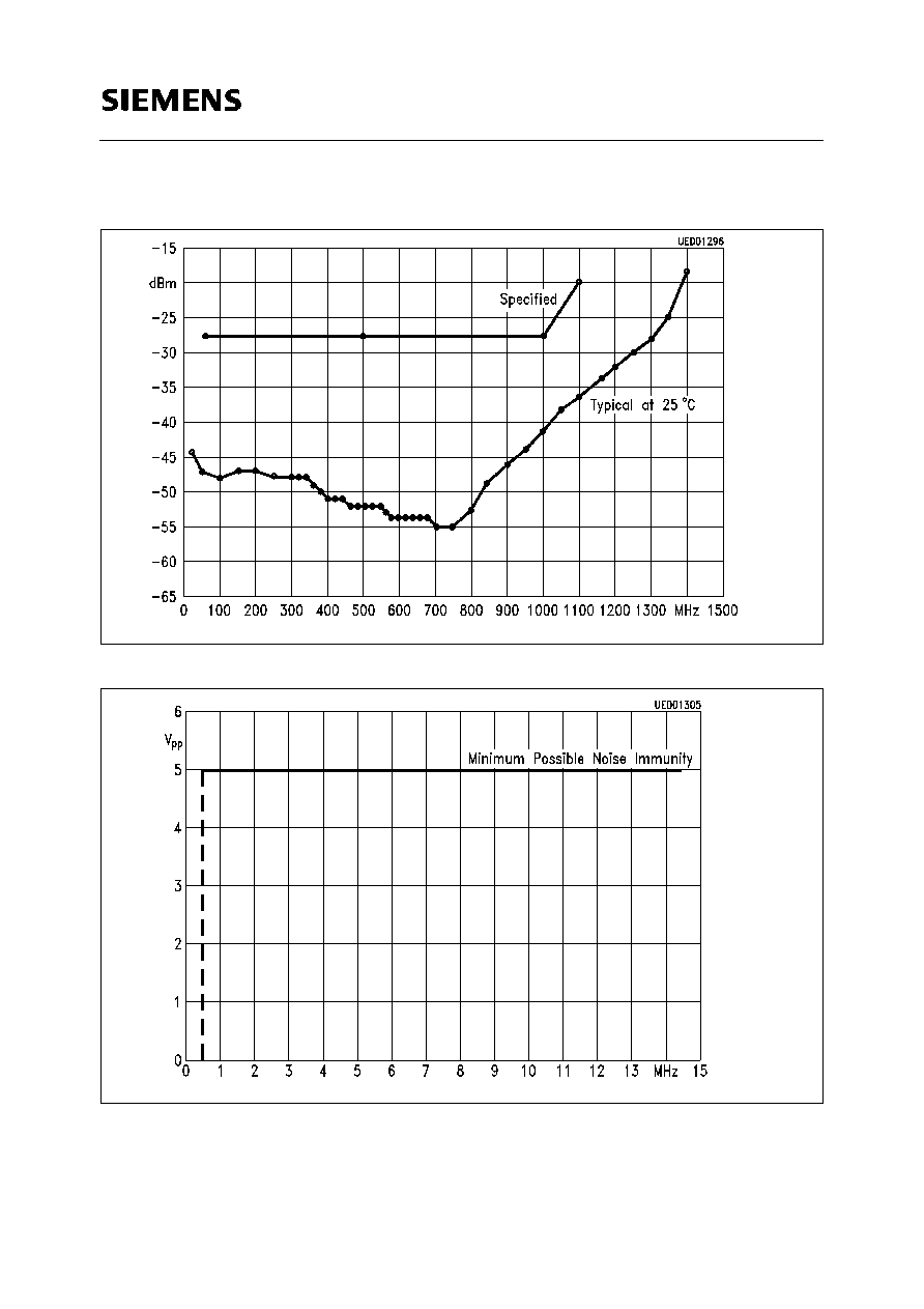
Sensitivity at UHF/VHF-Input
I
2
C Bus Noise Immunity
Sinusoidal noise pulses are applied via a coupling capacitance of 33 pF to the SCL- and
SDA-inputs.
MGP 3006X6
Semiconductor Group
21
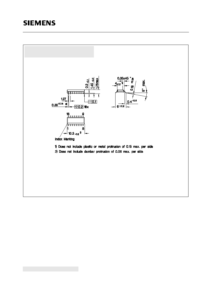
Plastic Package, P-DSO-16-1 (SMD)
(Plastic Dual Small Outline)
GPS05119
Sorts of Packing
Package outlines for tubes, trays etc. are contained in our
Data Book "Package Information"
Dimensions in mm
SMD = Surface Mounted Device