Semiconductor Group
1
04.97
Type
Ordering
Code
Tape and Reel
Information
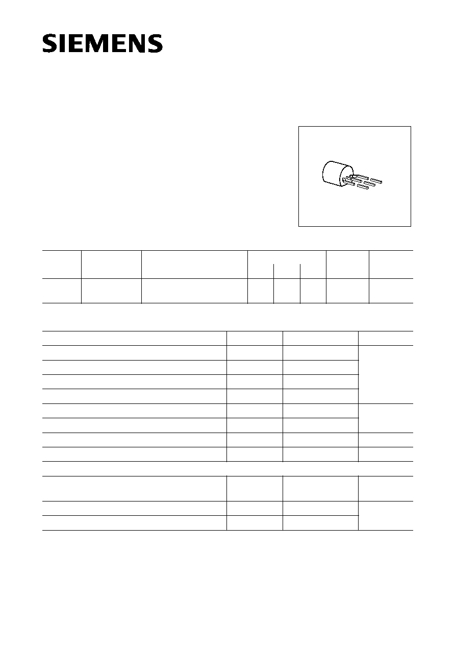
Pin Configuration Marking
Package
1
2
3
BSS 135
Q67000-S237 E6325: 2000 pcs/carton;
Ammopack
G
D
S
SS135
TO-92
Maximum Ratings
Parameter
Symbol
Values
Unit
Drain-source voltage
V
DS
600
V
Drain-gate voltage,
R
GS
= 20 k
V
DGR
600
Gate-source voltage
V
GS
±
14
Gate-source peak voltage, aperiodic
V
gs
±
20
Continuous drain current,
T
A
= 42 ∞C
I
D
0.080
A
Pulsed drain current,
T
A
= 25 ∞C
I
D puls
0.24
Max. power dissipation,
T
A
= 25 ∞C
P
tot
1.0
W
Operating and storage temperature range
T
j
,
T
stg
≠ 55 ... + 150
∞C
Thermal resistance, chip-ambient
(without heat sink)
R
thJA
125
K/W
DIN humidity category, DIN 40 040
≠
E
≠
IEC climatic category, DIN IEC 68-1
≠
55/150/56
SIPMOS
Æ
Small-Signal Transistor
BSS 135
1
2
3
q
V
DS
600 V
q
I
D
0.080 A
q
R
DS(on)
60
q
N channel
q
Depletion mode
q
High dynamic resistance
q
Available grouped in
V
GS(th)
Semiconductor Group
2
BSS 135
Electrical Characteristics
at
T
j
= 25 ∞C, unless otherwise specified.
Parameter
Symbol
Values
Unit
min.
typ.
max.
Static Characteristics
Drain-source breakdown voltage
V
GS
=
-
3 V,
I
D
= 0.25 mA
V
(BR)DSS
600
≠
≠
V
Gate threshold voltage
V
DS
= 3 V,
I
D
= 1 mA
V
GS(th)
-
1.8
-
1.5
-
0.7
Drain-source cutoff current
V
DS
= 600 V,
V
GS
=
-
3 V
T
j
= 25 ∞C
T
j
= 125 ∞C
I
DSS
≠
≠
≠
≠
100
200
nA
µ
A
Gate-source leakage current
V
GS
= 20 V,
V
DS
= 0
I
GSS
≠
10
100
nA
Drain-source on-resistance
V
GS
= 0 V,
I
D
= 0.01 A
R
DS(on)
≠
40
60
Dynamic Characteristics
Forward transconductance
V
DS
2
◊
I
D
◊
R
DS(on)max
,
I
D
= 0.01 A
g
fs
0.01
0.04
≠
S
Input capacitance
V
GS
=
-
3 V,
V
DS
= 25 V,
f
= 1 MHz
C
i
iss
≠
110
150
pF
Output capacitance
V
GS
=
-
3 V,
V
DS
= 25 V,
f
= 1 MHz
C
oss
≠
8
12
Reverse transfer capacitance
V
GS
=
-
3 V,
V
DS
= 25 V,
f
= 1 MHz
C
rss
≠
3
5
Turn-on time
t
on
, (
t
on
=
t
d(on)
+
t
r
)
t
d(on)
≠
4
6
ns
V
DD
= 30 V,
V
GS
=
-
3 V ... + 5 V,
R
GS
= 50
,
I
D
= 0.2 A
t
r
≠
10
15
Turn-off time
t
off
, (
t
off
=
t
d(off)
+
t
f
)
t
d(off)
≠
15
20
V
DD
= 30 V,
V
GS
=
-
3 V ... + 5 V,
R
GS
= 50
,
I
D
= 0.2 A
t
f
≠
20
30
Semiconductor Group
3
1) A specific group cannot be ordered separately.
Each reel only contains transistors from one group.
Electrical Characteristics (cont'd)
at
T
j
= 25 ∞C, unless otherwise specified.
Parameter
Symbol
Values
Unit
min.
typ.
max.
Reverse Diode
Continuous reverse drain current
T
A
= 25 ∞C
I
S
≠
≠
0.080
A
Pulsed reverse drain current
T
A
= 25 ∞C
I
SM
≠
≠
0.240
Diode forward on-voltage
I
F
= 0.16 A,
V
GS
= 0
V
SD
≠
0.80
1.30
V
V
GS(th)
Grouping
Symbol
Limit Values
Unit
Test Condition
min.
max.
Range of
V
GS(th)
V
GS(th)
≠
0.15
V
≠
Threshold voltage selected in groups
1)
:
P
R
S
T
U
V
W
V
GS(th)
≠ 0.95
≠ 1.08
≠ 1.21
≠ 1.34
≠ 1.47
≠ 1.60
≠ 1.73
≠ 0.80
≠ 0.93
≠ 1.06
≠ 1.19
≠ 1.32
≠ 1.45
≠ 1.58
V
V
V
V
V
V
V
V
DS1
= 0.2 V;
V
DS2
= 3 V;
I
D
= 1 mA
BSS 135
Semiconductor Group
4
Characteristics
at
T
j
= 25 ∞C, unless otherwise specified.
Total power dissipation
P
tot
=
f
(
T
A
)
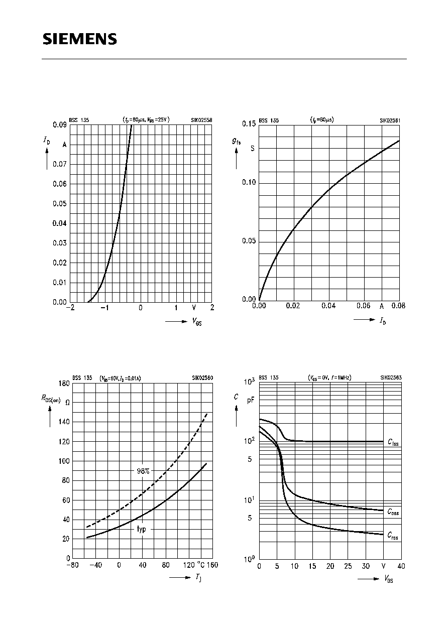
Typ. output characteristics
I
D
=
f
(
V
DS
)
parameter:
t
p
= 80
µ
s
Safe operating area
I
D
=
f
(
V
DS
)
parameter:
D
= 0.01,
T
C
= 25 ∞C
Typ. drain-source on-resistance
R
DS(on)
=
f
(
I
D
)
parameter:
V
GS
BSS 135
Semiconductor Group
5
Typ. transfer characteristics
I
D
=
f
(
V
GS
)
parameter:
t
p
= 80
µ
s,
V
DS
2
◊
I
D
◊
R
DS(on)max.
Drain-source on-resistance
R
DS(on)
=
f
(
T
j
)
parameter:
I
D
= 0.01 A,
V
GS
= 0 V, (spread)
Typ. forward transconductance
g
fs
=
f
(
I
D
)
parameter:
V
DS
2
◊
I
D
◊
R
DS(on)max.
,
t
p
= 80
µ
s
Typ. capacitances
C
=
f
(
V
DS
)
parameter:
V
GS
= 0,
f
= 1 MHz
BSS 135
Semiconductor Group
6
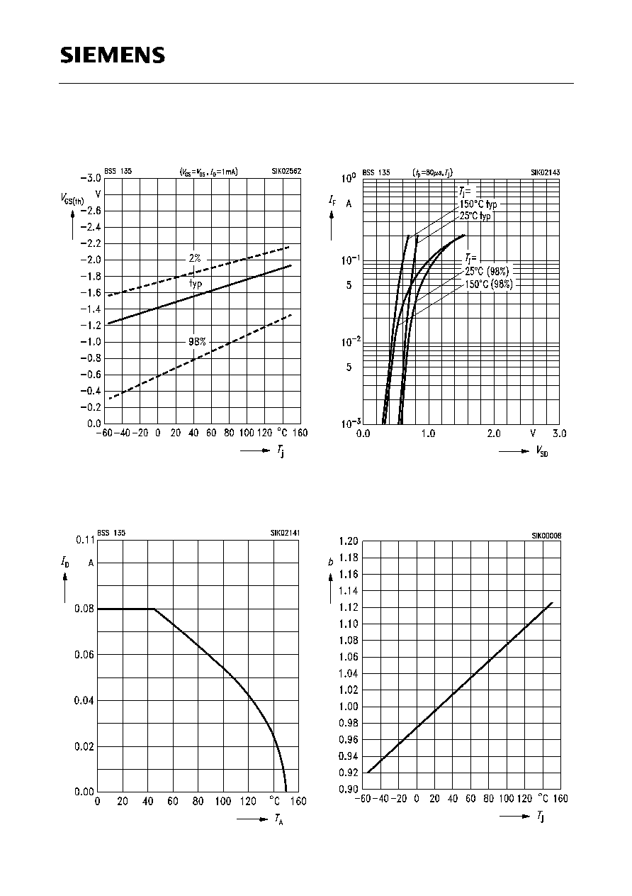
Gate threshold voltage
V
GS(th)
=
f
(
T
j
)
parameter:
V
DS
= 3 V,
I
D
= 1 mA, (spread)
Drain current
I
D
=
f
(
T
A
)
parameter:
V
GS
3 V
Forward characteristics of reverse diode
I
F
=
f
(
V
SD
)
parameter:
t
p
= 80
µ
s,
T
j
,
(spread)
Drain-source breakdown voltage
V
(BR) DSS
=
b
◊
V
(BR)DSS
(25 ∞C)
BSS 135