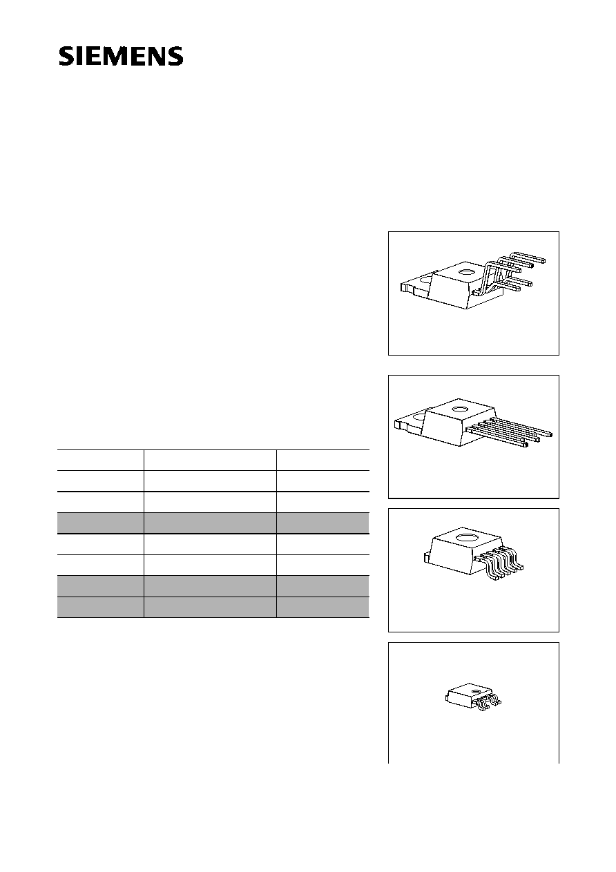
P-TO220-5-11
(P-TO220-5-1)
P-TO220-5-12
(P-TO220-5-2)
P-TO263-5-1
(P-TO220-5-8)
P-TO252-5-1 (D-PAK)
5-V Low-Drop Fixed Voltage Regulator
TLE 4270
Semiconductor Group
1
1998-11-01
Features
∑ Output voltage tolerance
±
2 %
∑ Low-drop voltage
∑ Integrated overtemperature protection
∑ Reverse polarity protection
∑ Input voltage up to 42 V
∑ Overvoltage protection up to 65 V (
400 ms)
∑ Short-circuit proof
∑ Suitable for use in automotive electronics
∑ Wide temperature range
∑ Adjustable reset time
∑ ESD protection
>
4000 V
w
Not for new design
q
New type
Functional Description
This device is a 5-V low-drop fixed-voltage regulator.
The maximum input voltage is 42 V (65 V,
400 ms).
Up to an input voltage of 26 V and for an output current
up to 550 mA it regulates the output voltage within a
2 % accuracy. The short circuit protection limits the
Type
Ordering Code
Package
TLE 4270
Q67000-A9209-A903 P-TO220-5-11
TLE 4270 S
Q67000-A9243-A904 P-TO220-5-12
TLE 4270 G
Q67006-A9201-A901 P-TO263-5-1
w
TLE 4270
Q67000-A9209-A801 P-TO220-5-1
w
TLE 4270 S
Q67000-A9243-A802 P-TO220-5-2
w
TLE 4270 G
Q67006-A9201-A802 P-TO220-5-8
q
TLE 4270 D
Q67006-A9360
P-TO252-5-1
output current of more than 650 mA. The device incorporates overvoltage protection
and temperature protection that disables the circuit at unpermissibly high temperatures.

TLE 4270
Semiconductor Group
2
1998-11-01
Pin Configuration
(top view)
Figure 1
Pin Definitions and Functions
Pin
Symbol
Function
1
I
Input; block to ground directly on the IC with ceramic capacitor
2
RO
Reset Output; the open collector output is connected to the 5 V output
via an integrated resistor of 30 k
.
3
GND
Ground; internally connected to heatsink.
4
D
Reset Delay; connect a capacitor to ground for delay time adjustment.
5
Q
5-V Output; block to ground with 22
µ
F capacitor, ESR
<
3
.
AEP01922
RO
GND
D
Q
1
5
P-TO263-5-1
(P-TO220-5-8)
AEP01923
RO
GND
D
Q
5
1
P-TO220-5-11
(P-TO220-5-1)
P-TO220-5-12
(P-TO220-5-2)
AEP02172
RO
GND
D
Q
5
1
P-TO252-5-1 (D-PAK)
AEP02580
1
5
RO
D Q
GND

TLE 4270
Semiconductor Group
3
1998-11-01
Application Description
The IC regulates an input voltage in the range of 5.5 V
<
V
I
<
36 V to
V
Qnom
= 5.0 V. Up
to 26 V it produces a regulated output current of more than 550 mA. Above 26 V the
save-operating-area protection allows operation up to 36 V with a regulated output
current of more than 300 mA. Overvoltage protection limits operation at 42 V. The
overvoltage protection hysteresis restores operation if the input voltage has dropped
below 36 V. A reset signal is generated for an output voltage of
V
Q
<
4.5 V. The delay for
power-on reset can be set externally with a capacitor.
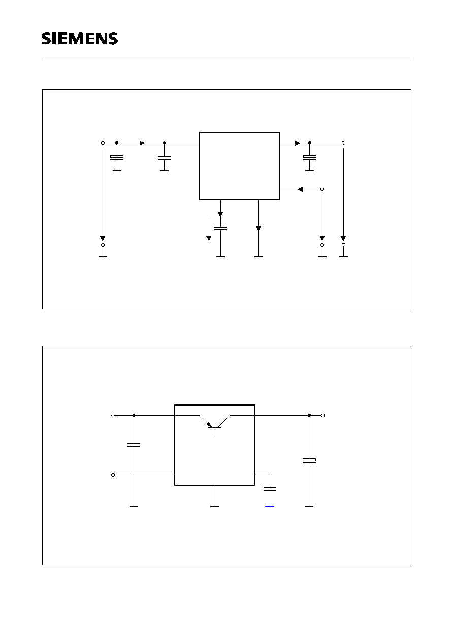
Design Notes for External Components
An input capacitor
C
I
is necessary for compensation of line influences. The resonant
circuit consisting of lead inductance and input capacitance can be damped by a resistor
of approx. 1
in series with
C
I
. An output capacitor
C
Q
is necessary for the stability of
the regulating circuit. Stability is guaranteed at values of
C
Q
22
µ
F and an ESR of
<
3
.
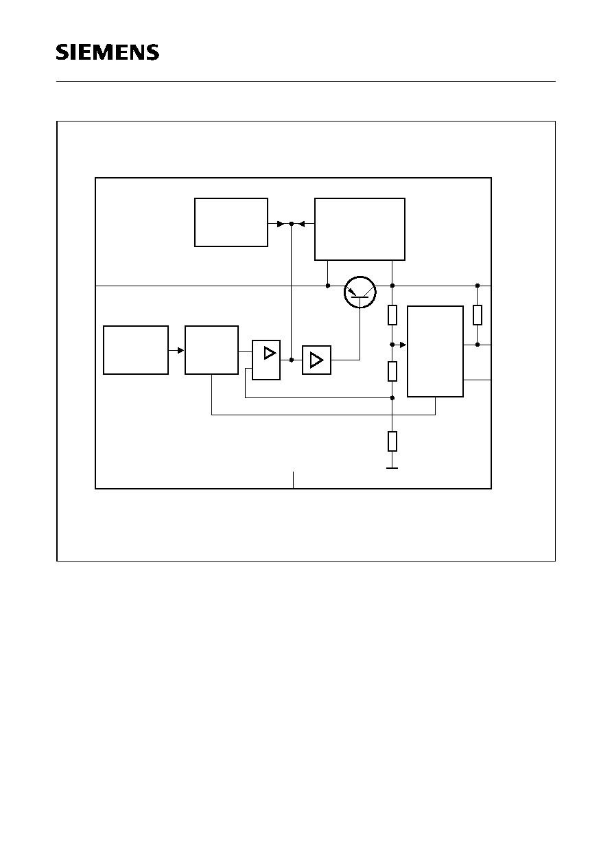
Circuit Description
The control amplifier compares a reference voltage, which is kept highly accurate by
resistance adjustment, to a voltage that is proportional to the output voltage and drives
the base of a series transistor via a buffer. Saturation control as a function of the load
current prevents any over-saturation of the power element.
If the output voltage decreases below 4.5 V, an external capacitor
C
D
on pin 4 (D) will be
discharged by the reset generator. If the voltage on this capacitor drops below
V
DRL
, a
reset signal is generated on pin 2 (RO), i.e. reset output is set low. If the output voltage
rises above 4.5 V,
C
D
will be charged with constant current. After the power-on-reset time
the voltage on the capacitor reaches
V
DU
and the reset output will be set high again. The
value of the power-on-reset time can be set within a wide range depending of the
capacitance of
C
D
.
The IC also incorporates a number of internal circuits for protection against:
∑ Overload
∑ Overvoltage
∑ Overtemperature
∑ Reverse polarity
TLE 4270
Semiconductor Group
4
1998-11-01
Figure 2
Block Diagram
Temperature
Sensor
Saturation
Control and
Protection
Circuit
+
-
Reference
Bandgap
Adjustment
3
1
5
2
4
GND
Output
Reset
Output
Delay
Reset
Input
AEB01924
Control
Amplifier
Buffer
Reset
Generator

TLE 4270
Semiconductor Group
5
1998-11-01
Optimum reliability and life time are guaranteed if the junction temperature does not
exceed 125
∞
C in operating mode. Operation at up to the maximum junction temperature
of 150
∞
C is possible in principle. Note, however, that operation at the maximum
permitted ratings could affect the reliability of the device.
Absolute Maximum Ratings
T
j
= ≠ 40 to 150
∞
C
Parameter
Symbol
Limit Values
Unit
Notes
min.
max.
Input
Voltage
Voltage
Current
V
I
V
I
I
I
≠ 42
42
65
V
V
t
400 ms
internally limited
Reset Output
Voltage
Current
V
R
I
R
≠ 0.3
7
V
Internally limited
Reset Delay
Voltage
Current
V
D
I
D
≠ 0.3
7
V
Internally limited
Output
Voltage
Current
V
Q
I
Q
≠ 1.0
16
V
Internally limited
Ground
Current
I
GND
≠ 0.5
≠
A
≠
Temperatures
Junction temperature
Storage temperature
T
j
T
stg
≠ 50
150
150
∞
C
∞
C
≠

TLE 4270
Semiconductor Group
6
1998-11-01
Operating Range
Parameter
Symbol
Limit Values
Unit
Notes
min.
max.
Input voltage
V
I
6
42
V
≠
Junction temperature
T
j
≠ 40
150
∞
C
≠
Thermal Resistance
Junction ambient
R
thja
≠
65
70
K/W
K/W
TO263, TO252
1)
1)
Soldered in, min. footprint
Junction case
R
thjc
Z
thjc
≠
3
2
K/W
K/W
t
<
1 ms
(TO-220/263
Packages)
Characteristics
V
I
= 13.5 V; ≠ 40
∞
C
T
j
=
125
∞
C (unless otherwise specified)
Parameter
Symbol
Limit Values
Unit
Test Condition
min.
typ.
max.
Output voltage
V
Q
4.90
5.00
5.10
V
5 mA
I
Q
550 mA;
6 V
V
I
26 V
Output voltage
V
Q
4.90
5.00
5.10
V
26 V
V
I
36 V;
I
Q
300 mA
Output current
limiting
I
Qmax
650
850
≠
mA
V
Q
= 0 V
Current
consumption
I
q
=
I
I
-
I
Q
I
q
≠
1
1.5
mA
I
Q
= 5 mA
Current
consumption
I
q
=
I
I
≠
I
Q
I
q
≠
55
75
mA
I
Q
= 550 mA
Current
consumption
I
q
=
I
I
≠
I
Q
I
q
≠
70
90
mA
I
Q
= 550 mA;
V
I
= 5 V
Drop voltage
V
dr
≠
350
700
mV
I
Q
= 550 mA
1)

TLE 4270
Semiconductor Group
7
1998-11-01
Load regulation
V
Q
≠
25
50
mV
I
Q
= 5 to 550 mA;
V
I
= 6 V
Supply voltage
regulation
V
Q
≠
12
25
mV
V
I
= 6 to 26 V
I
Q
= 5 mA
Power supply
Ripple rejection
PSRR
≠
54
≠
dB
f
r
= 100 Hz;
V
r
= 0.5
V
SS
Reset Generator
Switching threshold
V
RT
4.5
4.65
4.8
V
≠
Reset High voltage
V
ROH
4.5
≠
≠
V
≠
Reset low voltage
V
ROL
≠
60
≠
mV
R
intern
= 30 k
2)
;
1.0 V
V
Q
4.5 V
Reset low voltage
V
ROL
≠
200
400
mV
I
R
= 3 mA,
V
Q
= 4.4 V
Reset pull-up
R
18
30
46
k
internally connected
to Q
Lower reset timing
threshold
V
DRL
0.2
0.45
0.8
V
V
Q
<
V
RT
Charge current
I
d
8
14
25
µ
A
V
D
= 1.0 V
Upper timing
threshold
V
DU
1.4
1.8
2.3
V
≠
Delay time
t
d
≠
13
≠
ms
C
D
= 100 nF
Reset reaction time
t
RR
≠
≠
3
µ
s
C
D
= 100 nF
Overvoltage Protection
Turn-Off voltage
V
I
, ov
42
44
46
V
≠
1)
Drop voltage =
V
I
≠
V
Q
(measured when the output voltage has dropped 100 mV from the nominal value
obtained at 13.5 V input)
2)
Reset peak is always lower than 1.0 V.
Characteristics (cont'd)
V
I
= 13.5 V; ≠ 40
∞
C
T
j
=
125
∞
C (unless otherwise specified)
Parameter
Symbol
Limit Values
Unit
Test Condition
min.
typ.
max.
TLE 4270
Semiconductor Group
8
1998-11-01
Figure 3
Test Circuit
Figure 4
Application Circuit
2
V
V
C
D
D
4
D
3
GND
AES01925
R
V
V
Q
470 nF
1000 F
µ
TLE 4270G
1
5
Q
22 F
R
µ
Reset
to MC
2
3
4
AES01926
1
470 nF
Input
100 nF
22 F
TLE 4270
5
µ
5 V-Output

TLE 4270
Semiconductor Group
9
1998-11-01
Figure 5
Time Response
AES01927
d
=
d
d
V
d
C
t
<
t
RR
RR
t
t
d
D
V
V
Q
V
V
R
V
RT
V
DRL
DU
V
Power-on-Reset
Thermal
Shutdown
at Input
Voltage Drop Undervoltage
Spike
Secondary
Load
Bounce

TLE 4270
Semiconductor Group
10
1998-11-01
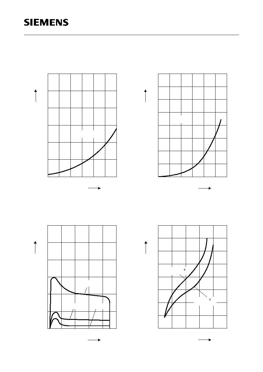
Output Voltage
V
Q
versus
Temperature
T
j
Output Current
I
Q
versus
Temperature
T
j
Output Voltage
V
Q
versus
Input Voltage
V
I
Output Current
I
Q
versus
Input Voltage
V
I
4.90
4.80
4.70
40
-40
0
4.60
5.00
V
5.20
5.10
Q
160
C
80
120
T
j
AED01928
V
= 13.5 V
V
600
400
200
40
-40
0
0
800
mA
1200
1000
Q
160
C
80
120
T
j
AED01930
R
6
4
2
0
4
0
2
8
12
10
Q
V
V
10
V
6
8
V
AED01929
= 25
L
0.6
0.4
0.2
20
0
10
0
0.8
A
1.2
1.0
Q
= 25 C
T
j
50
V
30
40
V
AED01931
= 125 C
T
j
TLE 4270
Semiconductor Group
11
1998-11-01
Current Consumption
I
q
versus Output Current
I
Q
Current Consumption
I
q
versus Input Voltage
V
I
Current Consumption
I
q
versus Output Current
I
Q
Drop Voltage
V
dr
versus
Output Current
I
Q
0
0
20
120
60
40
q
mA
AED01932
80
mA
1
2
3
4
5
6
Q
V
= 13.5 V
60
40
20
20
0
10
0
80
mA
120
100
q
50
V
30
40
V
AED01934
= 20
R
L
L
R = 50
R = 10
L
300
40
30
100
0
200
0
10
20
80
60
70
50
mA
q
V = 13.5 V
mA
400
600
Q
AED01933
400
200
300
100
200
0
400
0
800
600
700
500
Dr
V
mV
mA
600
1000
Q
AED01935
T = 125 C
j
T
=25
j
C

TLE 4270
Semiconductor Group
12
1998-11-01
Charge Current
I
d
versus Temperature
T
j
Delay Switching threshold
V
DU
versus Temperature
T
j
4
2
3
1
0
-40
40
0
8
6
7
5
d
A
C
120
80
160
T
j
AED01936
d
V
= 13.5 V
= 1 V
D
V
µ
2.0
1.0
1.5
0.5
0
-40
40
0
4.0
3.0
3.5
2.5
dT
V
V
C
120
80
160
T
j
AED01937
V = 13.5 V
DU
V

TLE 4270
Semiconductor Group
13
1998-11-01
Package Outlines
10
+0.4
3.75
+0.1
1
5
1.7
0.8
8.4
±0.4
±0.4
4.5
0.4
+0.1
10.2
15.4
±0.3
8.8
-0.2
16
1.27
+0.1
-0.2
10.2
+0.1
2.8
4.6
-0.2
2.6
8.6
±0.3
±0.3
±0.4
19.5 max
1x45∞
1)
1) 1 at dam bar (max 1.8 from body)
1) 1 im Dichtstegbereich (max 1.8 vom Kˆrper)
-0.15
-0.15
M
0.6
5x
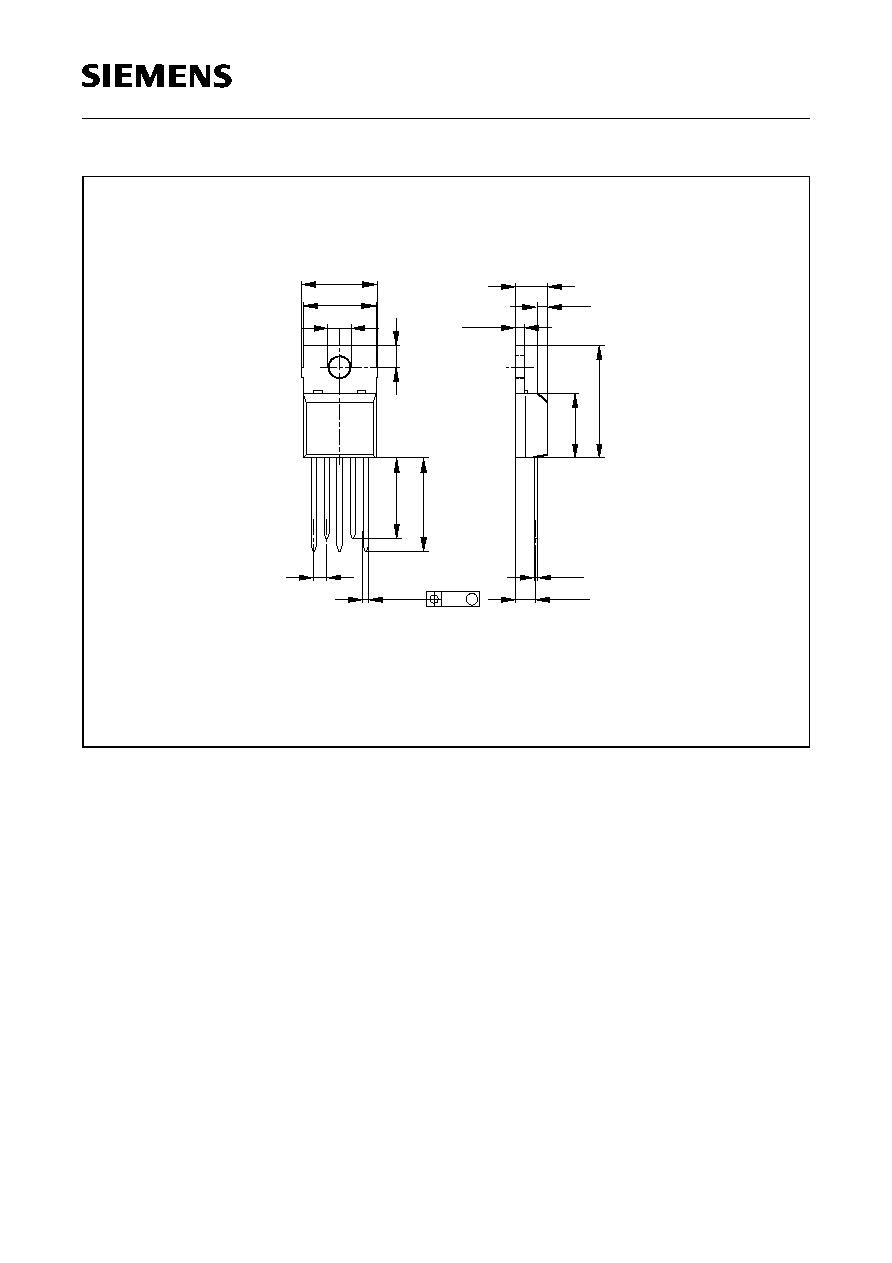
P-TO220-5-1
(Plastic Transistor Single Outline)
GP
T
0
510
7
Sorts of Packing
Package outlines for tubes, trays etc. are contained in our
Data Book "Package Information".
Dimensions in mm
TLE 4270
Semiconductor Group
14
1998-11-01
Sorts of Packing
Package outlines for tubes, trays etc. are contained in our
Data Book "Package Information".
Dimensions in mm
10
+0.4
3.75
+0.1
1
5
1.7
0.8
±0.15
0.4
+0.1
15.4
±0.3
8.8
-0.2
1.27
+0.1
-0.2
10.2
+0.1
2.8
4.6
-0.2
2.6
10.9
±0.2
±0.2
12.9
1x45∞
1)
1) 1 at dam bar (max 1.8 from body)
1) 1 im Dichtstegbereich (max 1.8 vom Kˆrper)
-0.15
-0.15
M
0.6
5x
P-TO220-5-2
(Plastic Transistor Single Outline)
GP
T
0
525
6

TLE 4270
Semiconductor Group
15
1998-11-01
GPT09064
A
A
0.25
M
Typical
9.8
±0.15
2.8
1)
15.65
±0.3
13.4
0...0.15
1.7
0.8
±0.1
±0.1
1.27
4.4
9.25
±0.2
0.05
1)
All metal surfaces tin plated, except area of cut.
C
±0.2
17
±0.3
8.5
1)
10
±0.2
3.7
-0.15
C
2.4
0.5
±0.1
±0.3
8.6
10.2
±0.3
±0.4
3.9
±0.4
8.4
3.7
±0.3
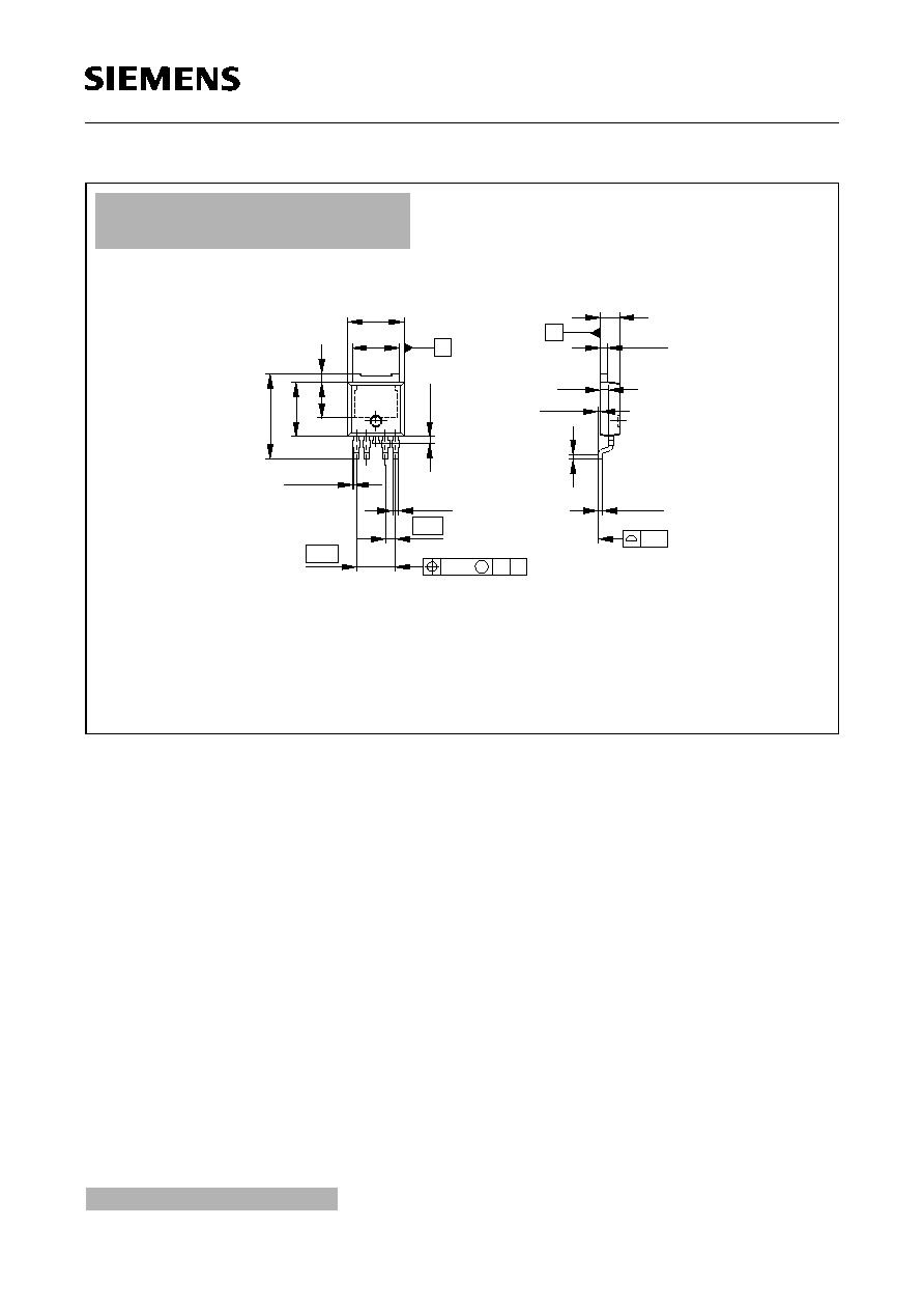
P-TO220-5-11
(Plastic Transistor Single Outline)
Sorts of Packing
Package outlines for tubes, trays etc. are contained in our
Data Book "Package Information".
Dimensions in mm

TLE 4270
Semiconductor Group
16
1998-11-01
GPT09065
A
B
A
0.25
M
Typical
9.8
±0.15
2.8
1)
15.65
±0.3
13.4
0...0.15
1.7
0.8
±0.1
±0.1
1.27
4.4
B
9.25
±0.2
0.05
1)
All metal surfaces tin plated, except area of cut.
C
±0.2
17
±0.3
8.5
1)
10
±0.2
3.7
-0.15
C
2.4
0.5
±0.1
13
±0.5
±0.5
11
6x
P-TO220-5-12
(Plastic Transistor Single Outline)
Sorts of Packing
Package outlines for tubes, trays etc. are contained in our
Data Book "Package Information".
Dimensions in mm

TLE 4270
Semiconductor Group
17
1998-11-01
A
8∞ max.
B
A
0.25
M
0.1
Typical
9.8
±0.15
±0.2
10
8.5
1)
8
1)
(15)
±0.2
9.25
±0.3
1
0...0.15
5x0.8
±0.1
±0.1
1.27
4.4
B
0.5
±0.1
±0.3
2.7
4.7
±0.5
0.05
1)
0.1
All metal surfaces tin plated, except area of cut.
2.4
4x1.7
P-TO263-5-1
(Plastic Transistor Single Outline)
G
P
T
0
9
113
Sorts of Packing
Package outlines for tubes, trays etc. are contained in our
Data Book "Package Information".
Dimensions in mm
SMD = Surface Mounted Device

TLE 4270
Semiconductor Group
18
1998-11-01
GPT05873
10.2
8.0
10.1
0.8
4 x 1.7 = 6.8
3.5
0.4
8.8
1.5
0.2
1.27
2.6
4.6
1.7
1)
1) shear and punch direction burr free surface
P-TO220-5-8
(Plastic Transistor Single Outline)
Sorts of Packing
Package outlines for tubes, trays etc. are contained in our
Data Book "Package Information".
Dimensions in mm
SMD = Surface Mounted Device
TLE 4270
Semiconductor Group
19
1998-11-01
Sorts of Packing
Package outlines for tubes, trays etc. are contained in our
Data Book "Package Information".
Dimensions in mm
SMD = Surface Mounted Device
GPT09161
5.4
±0.1
-0.10
6.5
+0.15
A
±0.5
9.9
6.22
-0.2
1
±0.1
±0.15
0.8
0.15 max
±0.1
per side
5x0.6
1.14
4.56
+0.08
-0.04
0.9
2.3
-0.10
+0.05
B
0.51 min
±0.1
1
+0.08
-0.04
0.5
0...0.15
B
A
0.25
M
0.1
All metal surfaces tin plated, except area of cut.
(4.17)
P-TO252-5-1
(Plastic Transistor Single Outline)