P-DSO-14-4
Semiconductor Group
1
1998-11-01
5-V Low-Drop Fixed Voltage Regulator
TLE 4278 G
Features
∑ Output voltage tolerance
±
2%
∑ Very low current consumption
∑ Separated reset and watchdog output
∑ Low-drop voltage
∑ Watchdog
∑ Adjustable watchdog activating threshold
∑ Settable reset threshold
∑ Overtemperature protection
∑ Reverse polarity protection
∑ Short-circuit proof
∑ Suitable for use in automotive electronics
∑ Wide temperature range
Functional Description
The TLE 4278 is a monolithic integrated low-drop fixed-voltage regulator which can
supply loads up to 200 mA. The device is available in the P-DSO-14-4 package. It is
designed to supply microprocessor systems under the severe conditions of automotive
applications and therefore is equipped with additional protection functions against over
load, short circuit and over temperature. Of course the TLE 4278 can also be used in
other applications where a stabilized voltage is required.
An input voltage
V
I
in the range of 5.5 V
V
I
45 V is regulated to
V
Qrated
= 5 V within an
accuracy of
±
2%.
The device operates in the wide temperature range of
T
j
= ≠ 40 to 150
∞
C.
Type
Ordering Code
Package
TLE 4278 G
Q67006-A9291
P-DSO-14-4 (SMD)

TLE 4278 G
Semiconductor Group
2
1998-11-01
Two additional features of the TLE 4278 are a load dependent watchdog function as well
as a power on reset and under voltage reset function with an adjustable reset delay time
and adjustable reset switching threshold.
The watchdog function monitors whether the microcontroller is functioning appropriately,
including time base failures. In the case that there is no positive-going edge within a
certain pulse repetition-time the watchdog output is set to LOW. Programming of the
max. repetition time is done by the reset delay capacitor so that no additional external
components are necessary. To prevent the microcontroller from a automatic reset in
case of missing pulses, the watchdog output WO is separated from the reset output RO
for the TLE 4278. The watchdog output can be used as an interrupt signal for the
microcontroller. Pin WO can be externally connected to pin RO.
When the controller is set to sleep mode or low power mode its current consumption
drops and no watchdog pulses are created. In order to prevent the microcontroller from
unnecessary wake ups due to missing pulses at pin WI the watchdog feature can be
disabled as a function of the load. The switch off threshold is set by an external resistor
to pin WADJ. This function can also be used as a timer, which periodically wakes up the
controller. Therefore the pin WADJ has to be connected to the output Q.
The power on reset feature is necessary for a defined start of the microprocessor when
switching on the application. For a certain delay time after the output voltage of the
regulator has surpassed the reset threshold, a reset signal is generated. The delay time
is set by an external delay capacitor. The under voltage reset circuit supervises the
output voltage. In case VQ falls below the reset threshold the reset output is set LOW
after a short reaction time. The reset LOW signal is generated down to an output voltage
VQ of 1 V. In addition the reset switching threshold can be adjusted by an external
voltage divider. This feature is useful with microprocessors which guarantee a safe
operation down to voltages below the internally set reset threshold of 4.65 V typical.
TLE 4278 G
Semiconductor Group
3
1998-11-01
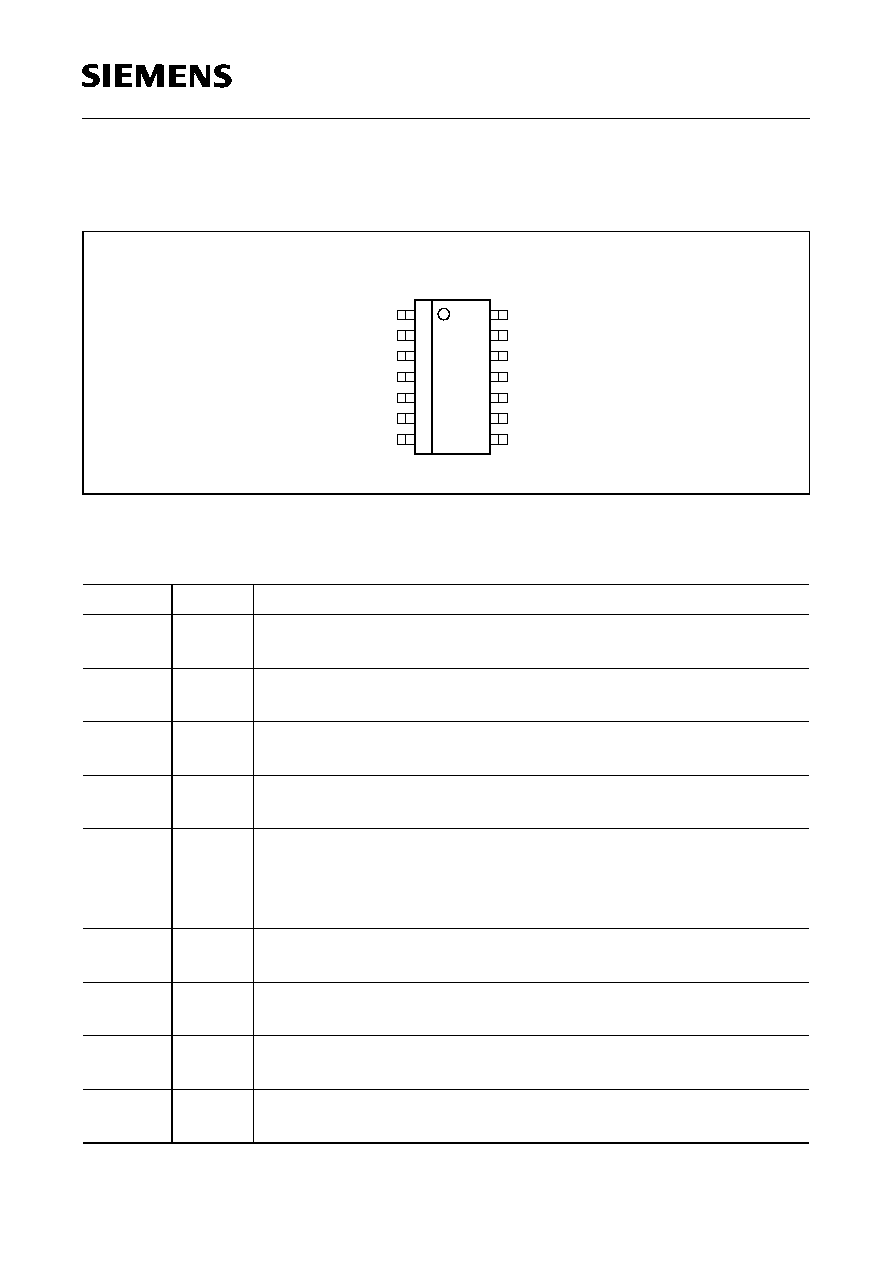
Pin Configuration
(top view)
Figure 1
Pin Definitions and Functions
Pin
Symbol Function
1
WO
Watchdog Output; the open collector output is connected to the
5-V output via an integrated resistor of 30 k
.
2
WADJ
Watchdog Adjust; an external resistor to GND determine the
watchdog activating threshold.
3, 4, 5,
10, 11, 12
GND
Ground
6
D
Reset Delay; connect a capacitor to ground for delay time
adjustment.
7
RADJ
Reset Switching Threshold Adjust; for setting the switching
threshold, connect a voltage divider from output to ground. If this
input is connected to ground, the reset is triggered at the internal
threshold.
8
WI
Watchdog input; positive-edge-triggered input for monitoring a
microcontroller.
9
V
Q
5-V output voltage; block to ground with min. 10
µ
F capacitor,
ESR
<
10
at 10 kHz.
13
V
I
Input voltage; block to ground directly on the IC with ceramic
capacitor.
14
RO
Reset output; the open collector output is connected to the
5-V output via an integrated resistor of 30 k
.
RO
GND
RADJ
D
GND
8
W
12
11
GND
GND
1
2
3
4
5
GND
6
7
14
13
WO
WADJ
9
10
AEP02113
GND
V
V
Q
P-DSO-14-4
TLE 4278 G
Semiconductor Group
4
1998-11-01
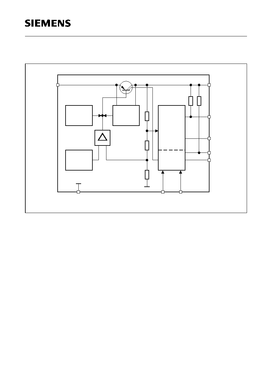
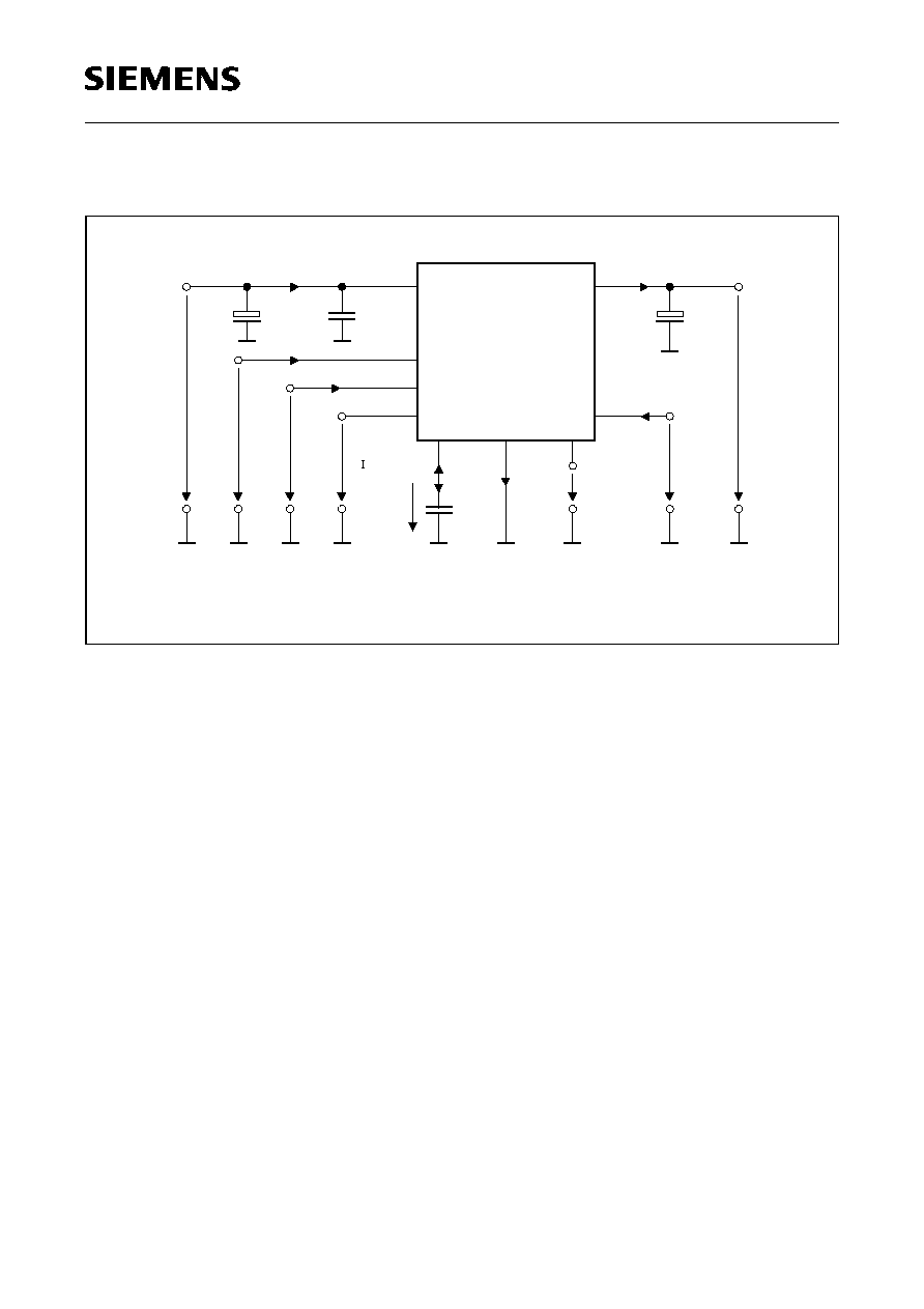
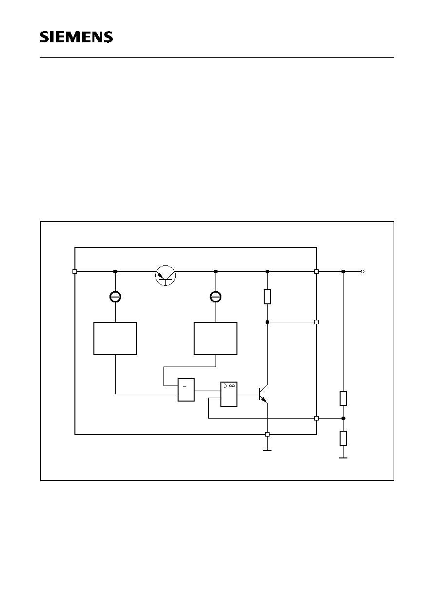
Block Diagram
Figure 2
AEB02114
Temperature
Sensor
-
+
Control
Amplifier
Protection
Circuit
Reference
Bandgap
Generator
Reset
Watchdog
W
14
12
7
6
V
RO
D
RADJ
13
3-5, 10-12
GND
8
2
WADJ
1
WO
V
Q
TLE 4278 G
Semiconductor Group
5
1998-11-01
Absolute Maximum Ratings
T
j
= ≠ 40 to 150
∞
C
Parameter
Symbol
Limit Values
Unit
Notes
min.
max.
Input Voltage
V
I
Voltage
V
I
≠ 42
45
V
≠
Current
I
I
≠
≠
mA
Internally limited
Output Voltage
V
Q
Voltage
V
Q
≠ 1
25
V
≠
Current
I
Q
≠
≠
mA
Internally limited
Reset Output RO
Voltage
V
RO
≠ 0.3
25
V
≠
Current
I
RO
≠ 5
5
mA
≠
Reset Delay D
Voltage
V
D
≠ 0.3
7
V
≠
Current
I
D
≠ 2
2
mA
≠
Reset Switching Threshold Adjust RADJ
Voltage
V
RADJ
≠ 0.3
7
V
≠
Current
I
RADJ
≠
≠
mA
Internally limited
Watchdog Input W
I
Voltage
V
W
I
≠ 0.3
7
V
≠
Current
I
W
I
≠
≠
mA
Internally limited
Watchdog Output WO
Voltage
V
WO
≠ 0.3
25
V
≠
Current
I
WO
≠ 5
5
mA
≠
TLE 4278 G
Semiconductor Group
6
1998-11-01
Note: ESD protection according to MIL Std. 883:
±
2 kV.
Maximum ratings are absolute ratings; exceeding any one of these values may
cause irreversible damage to the integrated circuit.
Operating Range
Note: In the operating range the functions given in the circuit description are fulfilled.
Watchdog Adjust WADJ
Voltage
V
WADJ
≠ 0.3
7
V
≠
Current
I
WADJ
≠
≠
mA
Internally limited
Ground GND
Current
I
GND
≠ 100
50
mA
≠
Temperatures
Junction temperature
T
j
≠ 50
150
∞
C
≠
Storage temperature
T
stg
≠ 50
150
∞
C
≠
Parameter
Symbol
Limit Values
Unit
Notes
min.
max.
Input voltage
V
I
5.5
45
V
≠
Junction temperature
T
j
≠ 40
150
∞
C
≠
Thermal Resistance
Junction ambient
R
thj-a
≠
70
K/W
Measured to pin 4
Junction pin
R
thj-pin
≠
25
K/W
Measured to pin 4
Absolute Maximum Ratings (cont'd)
T
j
= ≠ 40 to 150
∞
C
Parameter
Symbol
Limit Values
Unit
Notes
min.
max.
TLE 4278 G
Semiconductor Group
7
1998-11-01
Electrical Characteristics
V
I
= 13.5 V; ≠ 40
∞
C
T
j
125
∞
C (unless otherwise specified)
Parameter
Symbol
Limit Values
Unit Test Condition
min. typ.
max.
Output voltage
V
Q
4.90 5.00
5.10
V
1 mA
I
Q
150 mA;
6 V
V
I
28 V
Output voltage
V
Q
4.8
5.0
5.2
V
1 mA
I
Q
50 mA;
28 V
V
I
45 V
Output current limiting
I
Q
200
350
≠
mA
V
Q
= 4 V
Current consumption
I
q
=
I
I
≠
I
Q
I
q
≠
180
200
µ
A
T
j
= 25
∞
C;
I
Q
= 0 mA
Current consumption
I
q
=
I
I
≠
I
Q
I
q
≠
180
230
µ
A
I
Q
= 0 mA;
T
j
= 85
∞
C
Current consumption
I
q
=
I
I
≠
I
Q
I
q
≠
5
12
mA
I
Q
= 150 mA
Drop voltage;
V
DR
=
V
I
≠
V
Q
V
DR
≠
0.25
0.5
V
I
Q
= 150 mA
1)
Load regulation
V
Q
≠ 30 ≠ 5
≠
mV
I
Q
= 5 to 150 mA;
V
I
= 6 V
Supply voltage
regulation
V
Q
≠
5
20
mV
V
I
= 6 to 28 V
I
Q
= 5 mA
Reset Generator
Reset threshold
V
RT
4.5
4.65
4.8
V
RADJ connected to
GND
Reset headroom
V
Q,RT
180
300
≠
mV
I
Q
= 10 mA
Reset adjust threshold
V
RADJTH
1.28 1.35
1.45
V
V
Q
3.5 V
Reset low voltage
V
ROL
≠
0.20
0.40
V
R
ext
= 10 k
to
V
Q
V
Q
1 V
Reset high voltage
V
ROH
4.5
≠
≠
V
≠
Reset pull-up
R
RO
20
30
45
k
Internal connected to
V
Q
Charging current
I
d
2
5
8
µ
A
V
D
= 1.0 V
TLE 4278 G
Semiconductor Group
8
1998-11-01
Upper timing threshold
V
DU
1.5
1.9
2.3
V
≠
Lower reset timing
threshold
V
DRL
0.2
0.3
0.4
V
≠
Delay time
t
d
12
20
28
ms
C
D
= 47 nF
Reset reaction time
t
RR
0.4
1.0
2.0
µ
s
C
D
= 47 nF
Watchdog
Activating threshold
V
WADJ
1.28 1.35
1.45
V
Voltage at WADJ
Current ratio
I
Q
/
I
WADJ
650
720
800
≠
I
Q
10 mA
Slew rate
V
W
I
5
≠
≠
V/
µ
s From 20% up to 80%
V
Q
Watchdog low voltage
V
WOL
≠
0.2
0.4
V
R
ext
= 10 k
to
V
Q
Watchdog high voltage
V
WOH
4.5
≠
≠
V
≠
Watchdog pull-up
R
WO
20
30
45
k
Internal connected to
V
Q
Charge current
I
d
2
5
8
µ
A
V
D
= 1.0 V
Discharge current
I
dis
0.6
1.3
2.0
µ
A
V
D
= 1.0 V
Upper timing threshold
V
DU
1.5
1.9
2.3
V
≠
Lower watchdog timing
threshold
V
DWL
0.5
0.7
0.9
V
≠
Watchdog output period
T
WP
42
60
80
ms
C
d
= 47 nF
Watchdog output low
time
t
WR
7
13
19
ms
V
Q
>
V
RT
Watchdog trigger time
T
WT
35
47
61
ms
C
d
= 47 nF
1)
Measured when the output voltage
V
Q
has dropped 100 mV from the nominal value.
Electrical Characteristics (cont'd)
V
I
= 13.5 V; ≠ 40
∞
C
T
j
125
∞
C (unless otherwise specified)
Parameter
Symbol
Limit Values
Unit Test Condition
min. typ.
max.
TLE 4278 G
Semiconductor Group
9
1998-11-01
Test Circiut
Figure 3
AES02115
TLE 4278
1000 F
µ
nF
V
RO
O
V
d
GND
Q
C
D
47 nF
V
D
RO
O
V
-
V
V
DR
=
470
RE
V
V
W
V
Outside the control range
dis
V
RO
G
WADJ
WO
V
WADJ
WO
V
RADJ
GND
13
9
6
7
10-12
3-5,
D
1
2
8
14
WO
WADJ
Q
V
W
C
1
2
C
C
Q
10 F
µ

TLE 4278 G
Semiconductor Group
10
1998-11-01
Application Information
Input, Output
The input capacitors
C
I1
and
C
I2
are necessary for compensating line influences. Using
a resistor of approx. 1
in series with
C
I1
, the LC circuit of input inductivity and input
capacitance can be damped. To stabilize the regulation circuit the output capacitor
C
Q
is
necessary. Stability is guaranteed at values
C
Q
10
µ
F with an ESR
5
within the
operating temperature range.
Figure 4
Application Circuit
AES02116
TLE 4278G
C
D
47 nF
22 F
or short to GND
RADJ
WADJ
GND
13
9
6
2
10-12
3-5,
D
7
µ
+12 V
Cooling
Area
8
W
14
RO
WADJ
R
R
2
1
R
*)
*)
Q
C
for internal threshold
P
1
WO
V
V
Q
µ
470 nF
C
1
C
2
TLE 4278 G
Semiconductor Group
11
1998-11-01
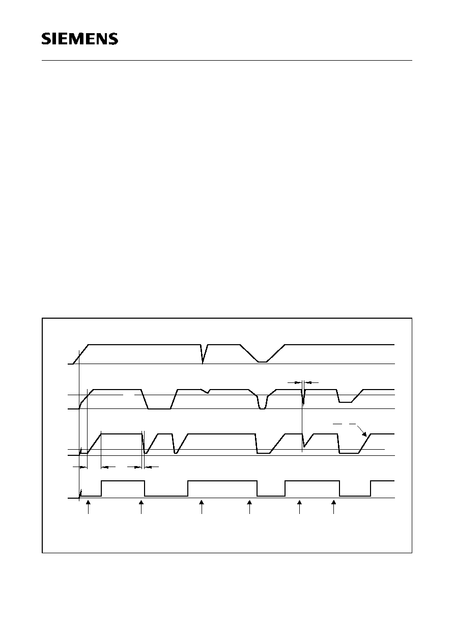
Reset Timing
The power-on reset delay time is defined by the charging time of an external capacitor
C
d
which can be calculated as follows:
C
d
= (
t
d
◊
I
d
)/
V
Definitions:
C
d
= delay capacitor
t
d
= delay time
I
d
= charge current, typical 5 mA
V
=
V
DU
, typical 1.9 V
V
DU
= upper delay switching threshold at
C
d
for reset delay time
The reset reaction time
t
rr
is the time it takes the voltage regulator to set the reset out
LOW after the output voltage has dropped below the reset threshold. It is typically 1
µ
s
for delay capacitor of 47 nF. For other values for
C
d
the reaction time can be estimated
using the following equation:
t
rr
20 s/F
◊
C
d
Figure 5
Reset Timing (Watchdog Disabled)
AED01542
Thermal
t
d
Power-on-Reset
Voltage Dip
Secondary
Overload
at Output
Spike
V
ST
V
V
D
V
RO
d
=
V
d
dt
V
Q
RT
V
t
RR
<
RR
t
V
DT
at Input
Undervoltage
Shutdown
C
D
TLE 4278 G
Semiconductor Group
12
1998-11-01
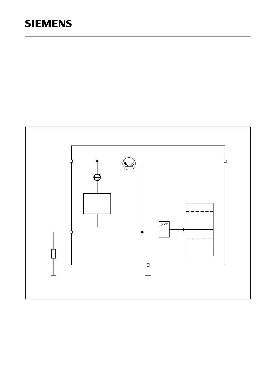
Reset Switching Threshold
The present default value is 4.65 V. When using the TLE 4278 the reset threshold can
be set to 3.5 V <
V
RTH
< 4.6 V by connecting an external voltage divider to pin RADJ. The
calculation can be easily done since the reset adjust input current can be neglected. If
this feature is unused, the pin can be left open or even better connected to GND.
R
1
=
R
2
◊
(
V
RTH
≠
V
ref
)/
V
ref
Definitions:
V
RT
= Reset threshold
V
ref
= comparator reference voltage, typical 1.35 V
(Reset adjust input current
50 nA)
Figure 6
The reset output pin is internally connected to the 5 V-output Q via a 30 k
pull-up
resistor. Down to an output voltage
V
Q
of typical 1 V the reset LOW signal at pin RO in
generated.
For the timing of the reset feature please refer to the data sheet, figure 5.
AES02553
Band-Gap-
Reference
V
RO
RADJ
GND
V
Q
Reference
Band-Gap-
> 1
+
-
1.35 V
1.35 V
30 k
R
1
2
R
TLE 4278 G
TLE 4278 G
Semiconductor Group
13
1998-11-01
Watchdog Activating
The calculation of the external resistor which adjusts the watchdog switch off threshold
can be done by the following equation.
R
WADJ
=
V
WADJ
◊
(
I
Q
/
I
WADJ
)/
I
QACT
Definitions:
V
WADJ
= switch off threshold, typical 1.35 V
I
Q
/
I
WADJ
= current ratio, typical 720
I
QACT
= switch off load current
Figure 7
AES02552
Band-Gap-
Reference
V
GND
V
Q
+
-
TLE 4278 G
Watchdog
active
HIGH
disabled
Watchdog
LOW
WADJ
R
WADJ
TLE 4278 G
Semiconductor Group
14
1998-11-01
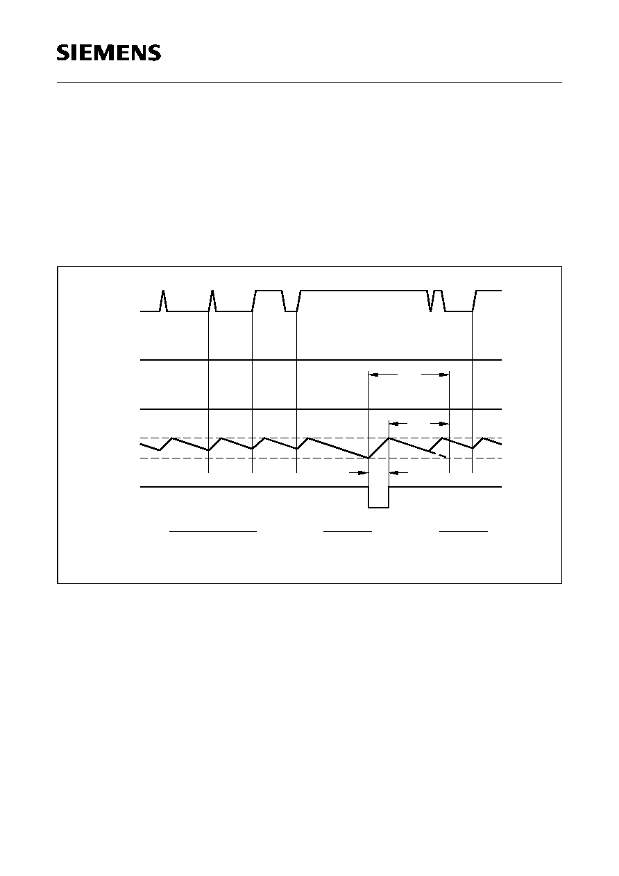
Watchdog Timing
The frequency of the watchdog pulses has to be higher than the minimum pulse
sequence which is set by the external reset delay capacitor
C
d
. Calculation can be done
according to the formulas given in figure 8.
The watchdog output is internally connected to the output Q via a 30 k
pull-up resistor.
To generate a watchdog created reset signal for the microcontroller the pin WO can be
connected to the reset input of the microcontroller. It is also allowed to parallel the
watchdog out to the reset out.
Figure 8
Timing of the Watchdog Function
AED01543
W
V
V
V
Q
D
V
V
WO
V
DU
-
V
DWL
(
)
(
d
+
dis
)
d
x
dis
T
WP
=
C
D
;
WR
t
WP
T
WT
T
WR
t
=
V
V
(
DU
-
DWL
)
d
D
C ;
T
=
V
V
(
DU
-
DWL
)
dis
D
C
DU
V
V
DWL
WT
DUL
V
=
DRL
V
TLE 4278 G
Semiconductor Group
15
1998-11-01
Hints for Unused Pins
Symbol
Function
Connect to
RO
Reset output
open
D
Reset delay
open or to output Q
RADJ
Reset switching threshold adjust
GND
WI
Watchdog input
GND
WO
Watchdog output
open
WADJ
Watchdog adjust
1)
to output Q via a 270 k
resistor:
Watchdog always active
2)
to GND: Watchdog disabled
TLE 4278 G
Semiconductor Group
16
1998-11-01
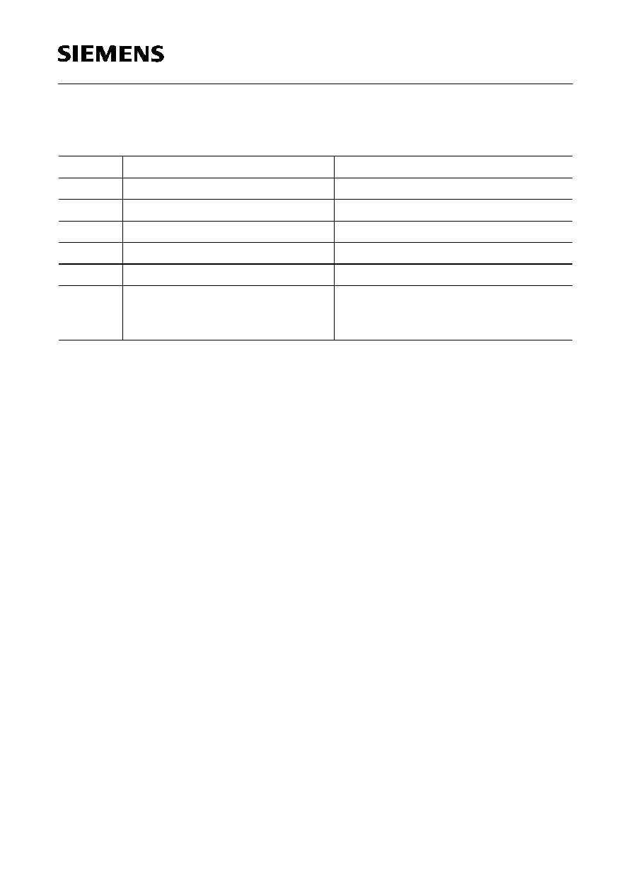
Drop Voltage
V
DR
versus
Output Current
I
Q
Current Consumption
I
q
versus Input Voltage
V
I
Current Consumption
I
q
versus Output Current
I
Q
Output Voltage
V
Q
versus
Input Voltage
V
I
AED01544
0
0
= 125
V
DR
T
mV
C
100
200
300
400
500
600
700
Q
50
100
150
200
mA
C
T
25
=
250
j
j
AED01546
0
0
= 33
R
q
V
2
4
6
8
10
mA
10
20
30
40
V
L
L
R
50
=
L
R
100
=
T
j
C
25
=
AED01545
0
50
150
200
0
2
6
10
12
14
Q
q
250
V
=13.5 V
mA
4
8
100
mA
T
25
=
j
C
AED01547
0
0
V
Q
V
2
4
6
8
10
mA
2
4
6
8
V
L
R
33
=
TLE 4278 G
Semiconductor Group
17
1998-11-01
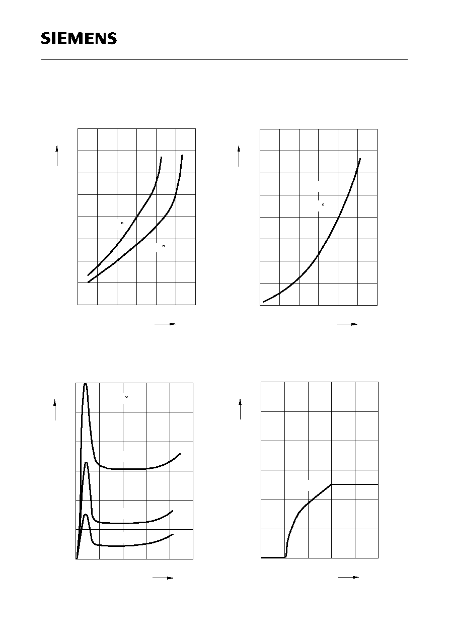
Charge Current
I
d
and Discharge
Current
I
dis
versus Temperature
T
j
Output Voltage
V
Q
versus
Temperature
T
j
Switching Voltage
V
DU,
V
DWL
and
V
DRL
versus Temperature
T
j
Output Current Limit
I
Q
versus
Input Voltage
V
I
AED01548
-40
0
= 13.5 V
T
A
0
40
80
120
C
V
1
2
3
4
5
6
7
µ
D
V
1.0 V
=
d
dis
j
AED01550
-40
4.6
V
Q
4.7
4.8
4.9
5.0
5.1
V
0
40
80
120
V
13.5 V
V
=
T
j
AED01549
-40
0
= 13.5 V
V
D
T
V
0
40
80
120
C
V
0.4
0.8
1.2
1.6
2.0
2.4
2.8
DU
V
DWL
V
V
DRL
j
AED01551
0
0
Q
50
100
150
200
250
mA
10
20
30
40
V
V
j
T
j
C
25
=
TLE 4278 G
Semiconductor Group
18
1998-11-01
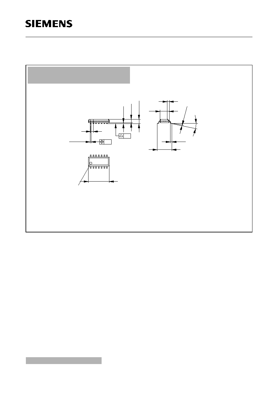
Package Outlines
1.27
1.45
-0.2
1
7
8.75
-0.2
14
8
1.75 max
0.2
6
±0.2
0.35 x 45∞
-0.2
4
0.1
-0.1
0.4
+0.8
Index Marking
1)
+0.15
0.35
2)
2) Does not include dambar protrusion of 0.05 max. per side
1) Does not include plastic or metal protrusion of 0.15 max. per side
0.2 14x
1)
0.19
+0.06
8∞ max.
GPS05093
P-DSO-14-4
(Plastic Dual Small Outline Package)
Sorts of Packing
Package outlines for tubes, trays etc. are contained in our
Data Book "Package Information".
Dimensions in mm
SMD = Surface Mounted Device