TLE 4266
Semiconductor Group
1
1998-11-01
5-V Low-Drop Voltage Regulator
Bipolar IC
Features
q
Output voltage tolerance
±
2 %
q
Very low current consumption
q
Low-drop voltage
q
Overtemperature protection
q
Reverse polarity proof
q
Wide temperature range
q
Suitable for use in automotive electronics
q
Inhibit
w
New type
Functional Description
TLE 4266 G is a 5-V low-drop voltage regulator in a P-SOT223-4-2 SMD package. The
IC regulates an input voltage
V
i
in the range of 5.5 V <
V
i
< 45 V to
V
Qrated
= 5 V / 10 V.
The maximum output current is more than 120 mA. The IC can be switched off via the
inhibit input, which causes the current consumption to drop below 10
µ
A. The IC is
shortcircuit-proof and incorporates temperature protection that disables the IC an
overtemperature.
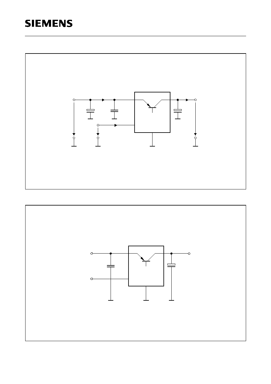
Dimensioning Information on External Components
The input capacitor
C
i
is necessary for compensating line influences. Using a resistor of
approx. 1
in series with
C
i
, the oscillating of input inductivity and input capacitance can
be clamped. The output capacitor
C
Q
is necessary for the stability of the regulating
circuit. Stability is guaranteed at values
C
Q
10
µ
F and an ESR
10
within the
operating temperature range.
Type
Ordering Code
Package
TLE 4266 G
Q67006-A9152
P-SOT223-4-2 (SMD)
w
TLE 4266 GSV10
Q67006-A9355
P-SOT223-4-2 (SMD)
P-SOT223-4-2
TLE 4266

TLE 4266
Semiconductor Group
2
1998-11-01
Pin Configuration
(top view)
Pin Definitions and Functions
Pin
Symbol
Function
1
V
I
Input voltage; block to ground directly at the IC with a ceramic
capacitor.
2
Inh
Inhibit; low-active input.
3
V
Q
Output voltage; block to ground with a
10
µ
F capacitor.
4
GND
Ground
AEP01734
V
Inh
Q
V
GND
1
2
3
4
TLE 4266
Semiconductor Group
3
1998-11-01
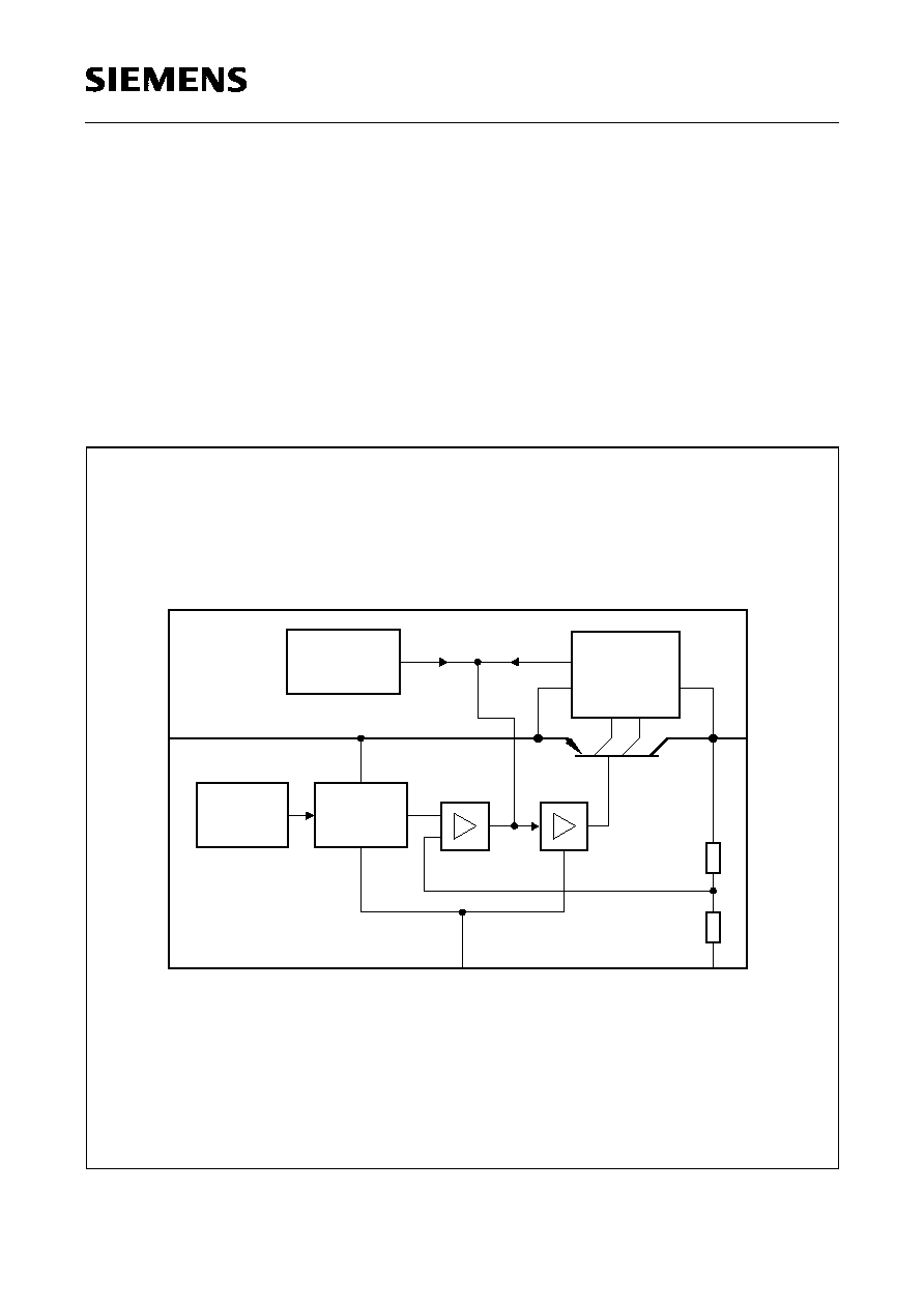
Circuit Description
The control amplifier compares a reference voltage, which is kept highly accurate by
resistance adjustment, to a voltage that is proportional to the output voltage and drives
the base of the series transistor via a buffer. Saturation control as a function of the load
current prevents any oversaturation of the power element. The IC also incorporates a
number of internal circuits for protection against:
q
Overload
q
Overtemperature
q
Reverse polarity
Block Diagram
4
2
Reference
Bandgap
Adjustment
Sensor
Temperature
Saturation
Control and
Protection
Circuit
Control
Amplifier
Buffer
1
3
Output
Input
Inhibit
GND
AEB01725
TLE 4266
Semiconductor Group
5
1998-11-01
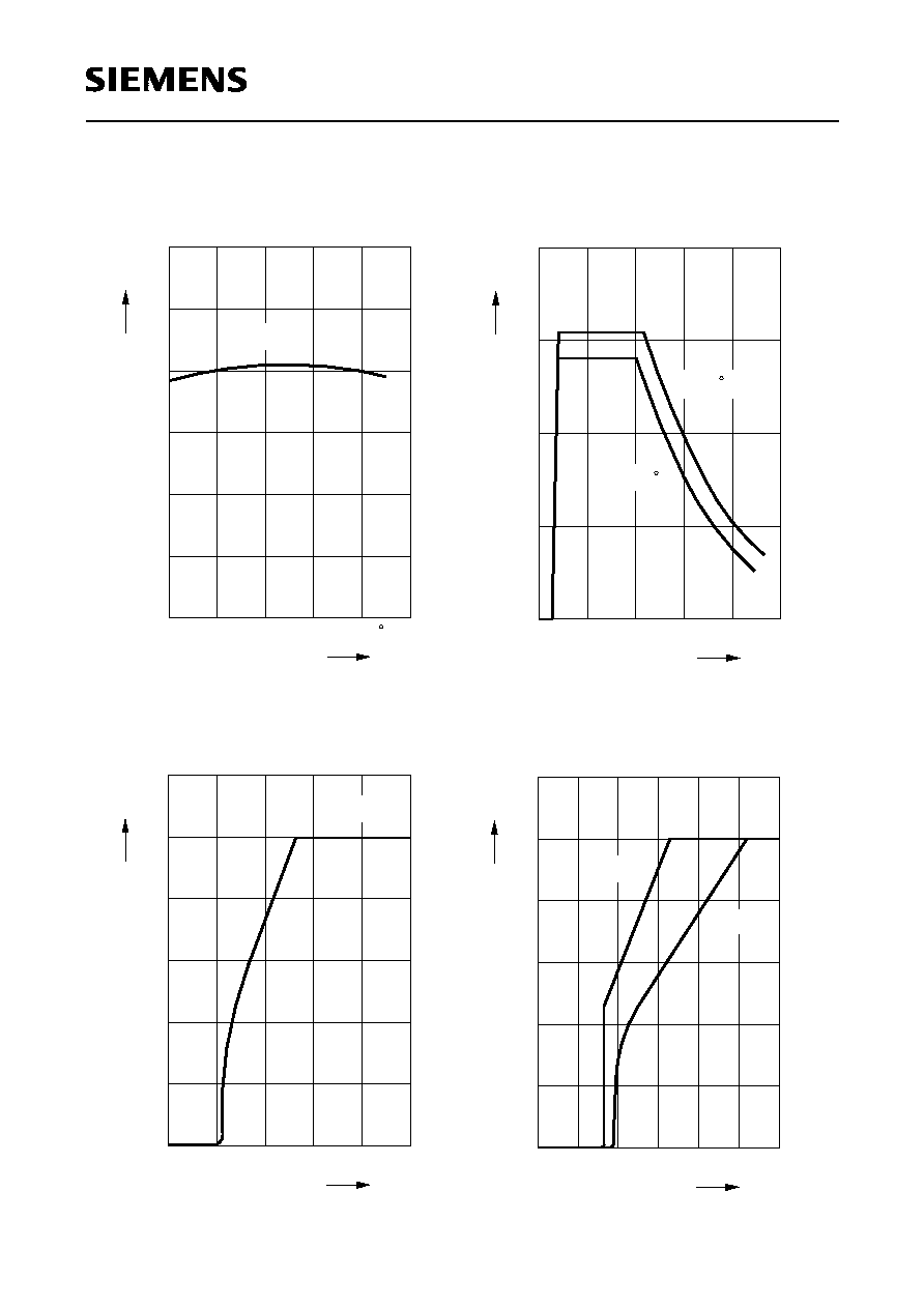
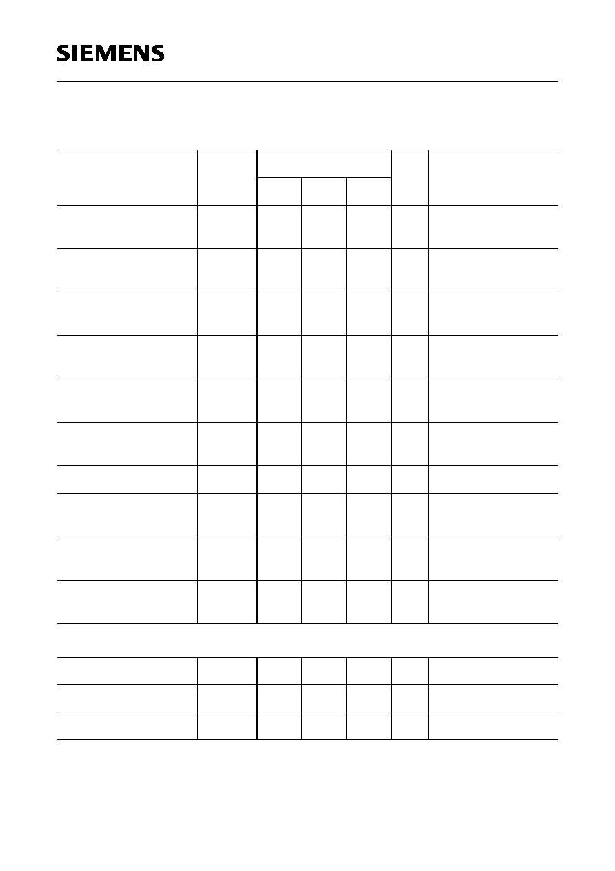
Characteristics
V
I
= 13.5 V; ≠ 40
∞
C
T
j
125
∞
C
Parameter
Symbol
Limit Values
Unit Test Condition
min.
typ.
max.
Output voltage
V
Q
4.9
5
5.1
V
5 mA
I
Q
100 mA
6 V
V
i
28 V
Output voltage
GSV 10-version
V
Q
9.8
10.0
10.2
V
5 mA
I
Q
100 mA
6 V
V
i
28 V
Output-current
limitation
I
Q
120
150
≠
mA
≠
Current consumption
I
q
=
I
i
≠
I
Q
I
q
≠
0
10
µ
A
V
e
= 0 V;
T
j
100
∞
C
Current consumption
I
q
=
I
i
≠
I
Q
I
q
≠
≠
400
µ
A
I
Q
= 1 mA
Current consumption
I
q
=
I
i
≠
I
Q
I
q
≠
10
15
mA
I
Q
= 100 mA
Drop voltage
V
Dr
≠
0.25
0.5
V
I
Q
= 100 mA
1)
Load regulation
V
Q
≠
≠
40
mV
I
Q
= 5 to 100 mA
V
i
= 6 V
Supply-voltage
regulation
V
Q
≠
15
30
mV
V
I
= 6 V to 28 V
I
Q
= 5 mA
Supply-voltage
rejection
SVR
≠
54
≠
dB
f
r
= 100 Hz
V
r
= 0.5
V
SS
Inhibit
Inhibit on voltage
V
e, on
≠
≠
3.5
V
≠
Inhibit off voltage
V
e, off
0.8
≠
≠
V
≠
Inhibit current
I
e
5
15
25
µ
A
V
e
= 5 V
1) Drop voltage =
V
i
≠
V
Q
(measured when the output voltage
V
Q
has dropped 100 mV from the
nominal value obtained at
V
i
= 13.5 V).

TLE 4266
Semiconductor Group
9
1998-11-01
Package Outlines
±0.1
±0.2
±0.1
0.7
4
3
2
1
6.5
3
acc. to
+0.2
DIN 6784
1.6
±0.1
15∞max
±0.04
0.28
7
±0.3
±0.2
3.5
0.5
0.1 max
min
B
M
0.25
B
A
2.3
4.6
A
M
0.25
P-SOT223-4-2
(Plastic Small Outline Transistor)
Weight approx. 0.15 g
GP
S05
560
Sorts of Packing
Package outlines for tubes, trays etc. are contained in our
Data Book "Package Information"
Dimensions in mm
SMD = Surface Mounted Device