
Standard EEPROM ICs
SLx 24C04/P
4 Kbit (512
◊
8 bit)
Serial CMOS-EEPROM with
I
2
C Synchronous 2-Wire Bus
and Page Protection Mode
TM
Data Sheet 1998-07-27

I
2
C Bus
Purchase of Siemens
I
2
C components conveys the license under the Philips
I
2
C patent to use the components in
the
I
2
C system provided the system conforms to the
I
2
C specifications defined by Philips.
Edition 1998-07-27
Published by Siemens AG,
Bereich Halbleiter, Marketing-
Kommunikation, Balanstraþe 73,
81541 M¸nchen
©
Siemens AG 1998.
All Rights Reserved.
Attention please!
As far as patents or other rights of third parties are concerned, liability is only assumed for components, not for applications, processes
and circuits implemented within components or assemblies.
The information describes the type of component and shall not be considered as assured characteristics.
Terms of delivery and rights to change design reserved.
For questions on technology, delivery and prices please contact the Semiconductor Group Offices in Germany or the Siemens Companies
and Representatives worldwide (see address list).
Due to technical requirements components may contain dangerous substances. For information on the types in question please contact
your nearest Siemens Office, Semiconductor Group.
Siemens AG is an approved CECC manufacturer.
Packing
Please use the recycling operators known to you. We can also help you ≠ get in touch with your nearest sales office. By agreement we
will take packing material back, if it is sorted. You must bear the costs of transport.
For packing material that is returned to us unsorted or which we are not obliged to accept, we shall have to invoice you for any costs in-
curred.
Components used in life-support devices or systems must be expressly authorized for such purpose!
Critical components
1
of the Semiconductor Group of Siemens AG, may only be used in life-support devices or systems
2
with the express
written approval of the Semiconductor Group of Siemens AG.
1 A critical component is a component used in a life-support device or system whose failure can reasonably be expected to cause the
failure of that life-support device or system, or to affect its safety or effectiveness of that device or system.
2 Life support devices or systems are intended (a) to be implanted in the human body, or (b) to support and/or maintain and sustain hu-
man life. If they fail, it is reasonable to assume that the health of the user may be endangered.
SLx 24C04/P
Revision History:
Current Version: 1998-07-27
Previous Version:
06.97
Page
(in previous
Version)
Page
(in current
Version)
Subjects (major changes since last revision)
3
3
Text was changed to "Typical programming time 5 ms for up to
16 bytes".
4, 5
4, 4
CS0, CS1 and CS2 were replaced by n.c.
5
≠
The paragraph "Chip Select (CS0, CS1, CS2)" was removed
completely.
5
5
WP =
V
CC
protects the upper half entire memory.
11, 12
11, 12
The erase/write cycle is finished latest after 10 8 ms.
15
15
Figure 11: second command byte is a CSR and not CSW.
21
21
The write or erase cycle is finished latest after 10 4 ms.
19
24
"Capacitive load ..." were added.
25
25
Some timings were changed.
25
25
The line "erase/write cycle" was removed.
25
25
Chapter 8.4 "Erase and Write Characteristics" has been added.
P-DIP-8-4
P-DSO-8-3
4 Kbit (512
◊
8 bit) Serial CMOS
EEPROMs,
I
2
C Synchronous 2-Wire Bus,
Page Protection Mode
TM
SLx 24C04/P
Semiconductor Group
3
1998-07-27
Features
∑ Data EEPROM internally organized as
512 bytes and 32 pages
◊
16 bytes
∑ Page protection mode, flexible page-by-page
hardware write protection
≠ Additional protection EEPROM of 32 bits, 1 bit per
data page
≠ Protection setting for each data page by writing its
protection bit
≠ Protection management without switching WP pin
∑ Low power CMOS
∑
V
CC
= 2.7 to 5.5 V operation
∑ Two wire serial interface bus,
I
2
C-Bus
compatible
∑ Filtered inputs for noise suppression with
Schmitt trigger
∑ Clock frequency up to 400 kHz
∑ High programming flexibility
≠ Internal programming voltage
≠ Self timed programming cycle including erase
≠ Byte-write and page-write programming, between 1 and 16 bytes
≠ Typical programming time 5 ms for up to 16 bytes
∑ High reliability
≠ Endurance 10
6
cycles
1)
≠ Data retention 40 years
1)
≠ ESD protection 4000 V on all pins
∑ 8 pin DIP/DSO packages
∑ Available for extended temperature ranges
≠ Industrial:
-
40 ∞C to + 85 ∞C
≠ Automotive:
-
40 ∞C to + 125 ∞C
1)
Values are temperature dependent, for further information please refer to your Siemens Sales office.
SLx 24C04/P
Semiconductor Group
4
1998-07-27
Ordering Information
Other types are available on request
≠ Temperature range (≠
55 ∞C
...
+ 150 ∞C)
≠ Package (die, wafer delivery)
1
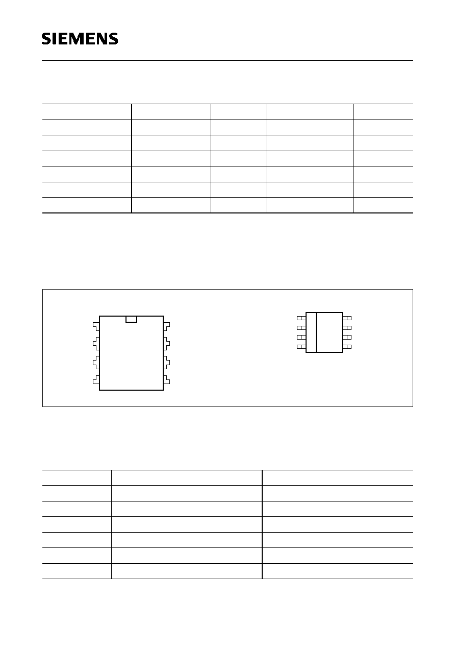
Pin Configuration
Figure 1
Pin Configuration (top view)
Pin Definitions and Functions
Type
Ordering Code
Package
Temperature
Voltage
SLA 24C04-D/P
Q67100-H3527
P-DIP-8-4
≠ 40 ∞C ... + 85 ∞C 4.5 V...5.5 V
SLA 24C04-S/P
Q67100-H3532
P-DSO-8-3 ≠ 40 ∞C ... + 85 ∞C 4.5 V...5.5 V
SLA 24C04-D-3/P
Q67100-H3526
P-DIP-8-4
≠ 40 ∞C ... + 85 ∞C 2.7 V...5.5 V
SLA 24C04-S-3/P
Q67100-H3531
P-DSO-8-3 ≠ 40 ∞C ... + 85 ∞C 2.7 V...5.5 V
SLE 24C04-D/P
Q67100-H3525
P-DIP-8-4
≠ 40∞C ... + 125 ∞C 4.5 V...5.5 V
SLE 24C04-S/P
Q67100-H3530
P-DSO-8-3 ≠ 40∞C ... + 125 ∞C 4.5 V...5.5 V
Table 1
Pin No.
Symbol
Function
1, 2, 3
N.C.
Not connected
4
V
SS
Ground
5
SDA
Serial bidirectional data bus
6
SCL
Serial clock input
7
WP
Write protection input
8
V
CC
Supply voltage
IEP02514
N.C.
5
6
7
8
4
3
2
1
V
SS
WP
SCL
SDA
CC
V
N.C.
N.C.
P-DSO-8-3
IEP02515
CC
V
1
8
WP
V
7
2
SCL
6
3
SDA
5
4
SS
N.C.
N.C.
N.C.
P-DIP-8-4

SLx 24C04/P
Semiconductor Group
5
1998-07-27
Pin Description
Serial Clock (SCL)
The SCL input is used to clock data into the device on the rising edge and to clock data
out of the device on the falling edge.
Serial Data (SDA)
SDA is a bidirectional pin used to transfer addresses, data or control information into the
device or to transfer data out of the device. The output is open drain, performing a wired
AND function with any number of other open drain or open collector devices. The SDA
bus requires a pull-up resistor to
V
CC
.
Write Protection (WP)
WP switched to
V
SS
allows normal read/write operations.
WP switched to
V
CC
protects the entire EEPROM against changes (hardware write
protection).
Additionally write protection is managed by a protection bit associated to each page.
(refer to chapter 7 Page Protection Mode
TM
)

SLx 24C04/P
Semiconductor Group
6
1998-07-27
2
Description
The SLx 24C04/P device is a serial electrically erasable and programmable read only
memory (EEPROM), organized as 512
◊
8 bit. The data memory is divided into
32 pages. The 16 bytes of a page can be programmed simultaneously. Each page may
be protected individually against changes by its associated protection bit.
The device conforms to the specification of the 2-wire serial
I
2
C-Bus. Low voltage design
permits operation down to 2.7 V with low active and standby currents.
The device operates at 5.0 V
±
10% with a maximum clock frequency of 400 kHz and at
2.7 ... 4.5 V with a maximum clock frequency of 100 kHz. The device is available as 5 V
type (
V
CC
= 4.5 ... 5.5 V) with two temperature ranges for industrial and automotive
applications and as 3 V type (
V
CC
= 2.7 ... 5.5 V) for industrial applications. The
EEPROMs are mounted in eight-pin DIP and DSO packages or are also supplied as
chips.
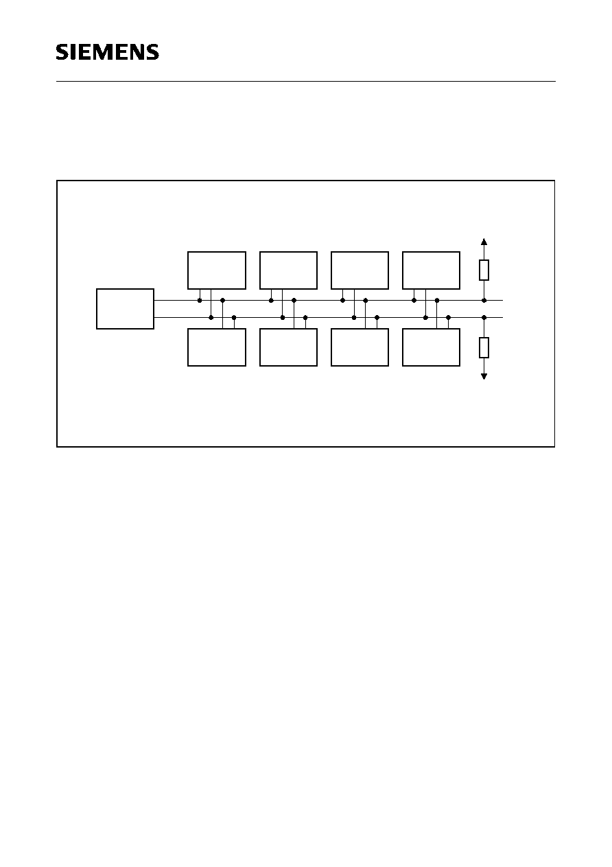
Figure 2
Block Diagram
DEC
X
EEPROM
Y DEC
Dout/ACK
SDA
SCL
IEB02531
Logic
Stop
Start/
Control
Chip Address
Logic
H.V. Pump
Programming
Control
Control
Serial
Logic
Logic
Address
Page Logic
SS
V
CC
V
WP
Prot. Bit
Page
EEPROM
SLx 24C04/P
Semiconductor Group
7
1998-07-27
3
I
2
C-Bus Characteristics
The SLx 24C04/P devices support a master/slave bidirectional bus oriented protocol in
which the EEPROM always takes the role of a slave.
Figure 3
Bus Configuration
Master
Device that initiates the transfer of data and provides the clock for both
transmit and receive operations.
Slave
Device addressed by the master, capable of receiving and transmitting
data.
Transmitter The device with the SDA as output is defined as the transmitter. Due to
the open drain characteristic of the SDA output the device applying a low
level wins.
Receiver
The device with the SDA as input is defined as the receiver.
Slave 1
Slave 2
Slave 3
Slave 4
Slave 8
Slave 5
Slave 6
Slave 7
Master
V
CC
CC
V
IES02183
SCL
SDA
SLx 24C04/P
Semiconductor Group
8
1998-07-27
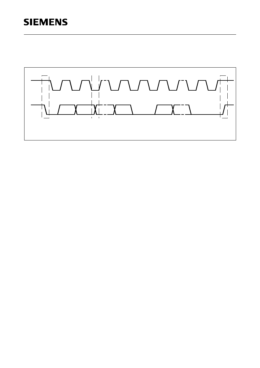
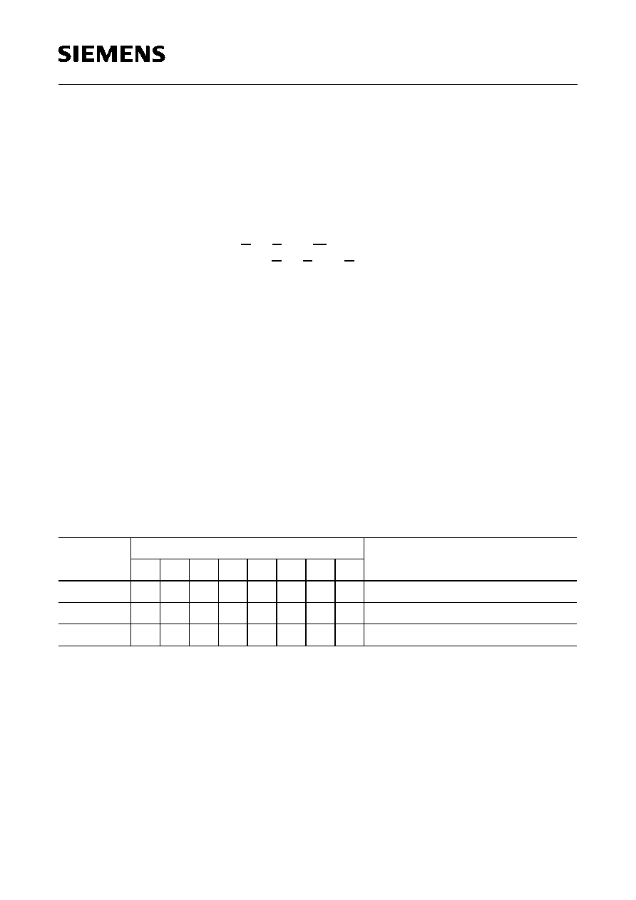
The conventions for the serial clock line and the bidirectional data line are shown in
figure 4.
Figure 4
I
2
C-Bus Timing Conventions for START Condition, STOP Condition, Data Valida-
tion and Transfer of Acknowledge ACK
Standby
Mode in which the bus is not busy (no serial transmission, no
programming): both clock (SCL) and data line (SDA) are in high
state. The device enters the standby mode after a STOP condition
or after a programming cycle.
START Condition
High to low transition of SDA when SCL is high, preceding all
commands.
STOP Condition
Low to high transition of SDA when SCL is high, terminating all
communications. A STOP condition initiates an EEPROM
programming cycle. A STOP condition after reading a data byte
from the EEPROM initiates the Standby mode.
Acknowledge
A successful reception of eight data bits is indicated by the
receiver by pulling down the SDA line during the following clock
cycle of SCL (ACK). The transmitter on the other hand has to
release the SDA line after the transmission of eight data bits.
The EEPROM as the receiving device responds with an
acknowledge, when addressed. The master, on the other side,
acknowledges each data byte transmitted by the EEPROM and
can at any time end a read operation by releasing the SDA line (no
ACK) followed by a STOP condition.
Data Transfer
Data must change only during low SCL state, data remains valid
on the SDA bus during high SCL state. Nine clock pulses are
required to transfer one data byte, the most significant bit (MSB)
is transmitted first.
1
2
8
9
1
9
ACK
ACK
START Condition
Data allowed
STOP Condition
to Change
Acknowledge
SCL
SDA
IED02128
SLx 24C04/P
Semiconductor Group
9
1998-07-27
4
Device Addressing and EEPROM Addressing
After a START condition, the master always transmits a Command Byte CSW or CSR.
After the acknowledge of the EEPROM a Control Byte follows, its content and the
transmitter depend on the previous Command Byte. The description of the Command
and Control Bytes is shown in table 2.
The device has an internal address counter which points to the current EEPROM
address.
The address counter is incremented
≠ after a data byte to be written has been acknowledged, during entry of further data
byte
≠ during a byte read, thus the address counter points to the following address after
reading a data byte.
Command Byte
Selects operation: the least significant bit b0 is low for a write
operation (Chip Select Write Command Byte CSW) or set high for a
read operation (Chip Select Read Command Byte CSR).
Contains address information: in the CSW Command Byte, the
bit position b1 is decoded for the uppermost EEPROM address bit
A8 (in the CSR Command Byte, the bit positions b3 to b1 are left
undefined, in the CSW Command Byte, the bit positions b3 and b2
as well).
Control Byte
Following CSW (b0 = 0): contains the eight lower bits of the
EEPROM address (EEA) bit A7 to A0, or an additional command
byte for the handling of the protection bit.
Following CSR (b0 = 1): contains the data read out, transmitted by
the EEPROM. The EEPROM data are read as long as the master
pulls down SDA after each byte in order to acknowledge the
transfer. The read operation is stopped by the master by releasing
SDA (no acknowledge is applied) followed by a STOP condition.
Table 2
Command and Control Byte for
I
2
C-Bus Addressing of Chip and EEPROM
Definition
Function
b7
b6
b5
b4
b3
b2
b1
b0
CSW
1
0
1
0
x
x
A8
0
Chip Select for Write
CSR
1
0
1
0
x
x
x
1
Chip Select for Read
EEA
A7
A6
A5
A4
A3
A2
A1
A0
EEPROM address

SLx 24C04/P
Semiconductor Group
10
1998-07-27
The timing conventions for read and write operations are described in figures 5 and 6.
Figure 5
Timing of the Command Byte CSW
Figure 6
Timing of the Command Byte CSR
1
2
3
4
5
6
7
8
9
10
11
12
13
14
15
16
17
18
1
0
1
0
X
X
A8
0
A7
A6
A5
A4
A3
A2
A1 A0 ACK
START from Master
Acknowledge from EEPROM
Acknowledge from EEPROM
SCL
SDA
Command Byte (CSW)
Data Transfer to EEPROM
IED02256
1
2
3
4
5
6
7
8
9
10
11
12
13
14
15
16
17
18
1
0
1
0
X
X
X
1
ACK
START from Master
Acknowledge from Master
Acknowledge from EEPROM
SCL
SDA
Command Byte (CSR)
Data Transfer from EEPROM
IED02185
ACK

SLx 24C04/P
Semiconductor Group
11
1998-07-27
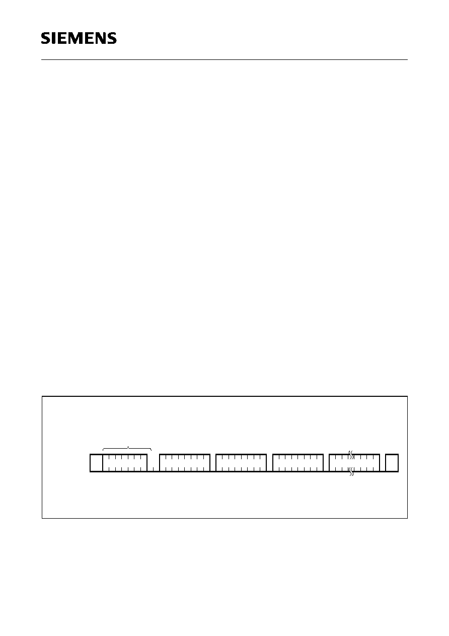
5
Write Operations
Changing of the EEPROM data is initiated by the master with the command byte CSW.
Depending on the state of the Write Protection pin WP and of the Protection Bits (refer
to chapter 7 Page Protection Mode
TM
) either one byte (Byte Write) or up to 16 bytes
(Page Write) are modified in one programming procedure.
5.1
Byte Write
Figure 7
Byte Write Sequence
The erase/write cycle is finished latest after 8 ms. Acknowledge polling may be used for
speed enhancement in order to indicate the end of the erase/write cycle (refer to
chapter 5.3 Acknowledge Polling).
Address Setting
After a START condition the master transmits the Chip Select
Write byte CSW. The EEPROM acknowledges the CSW byte
during the ninth clock cycle. The following byte with the
EEPROM address (A0 to A7) is loaded into the address
counter of the EEPROM and acknowledged by the EEPROM.
Transmission of Data
Finally the master transmits the data byte which is also
acknowledged by the EEPROM into the internal buffer.
Programming Cycle
Then the master applies a STOP condition which starts the
internal programming procedure. The data bytes are written in
the memory location addressed in the EEA byte (A0 to A7)
and the CSW byte (A8). The programming procedure consists
of an internally timed erase/write cycle. In the first step, the
selected byte is erased to "1". With the next internal step, the
addressed byte is written according to the contents of the
buffer.
Command Byte
CSW
S
P
C
K
A
C
K
A
S
T
A
R
T
T
P
O
S
EEPROM Address
EEA
Data Byte
Bus Activity
Master
SDA Line
Bus Activity
EEPROM
IED02129
C
K
A
0
SLx 24C04/P
Semiconductor Group
12
1998-07-27
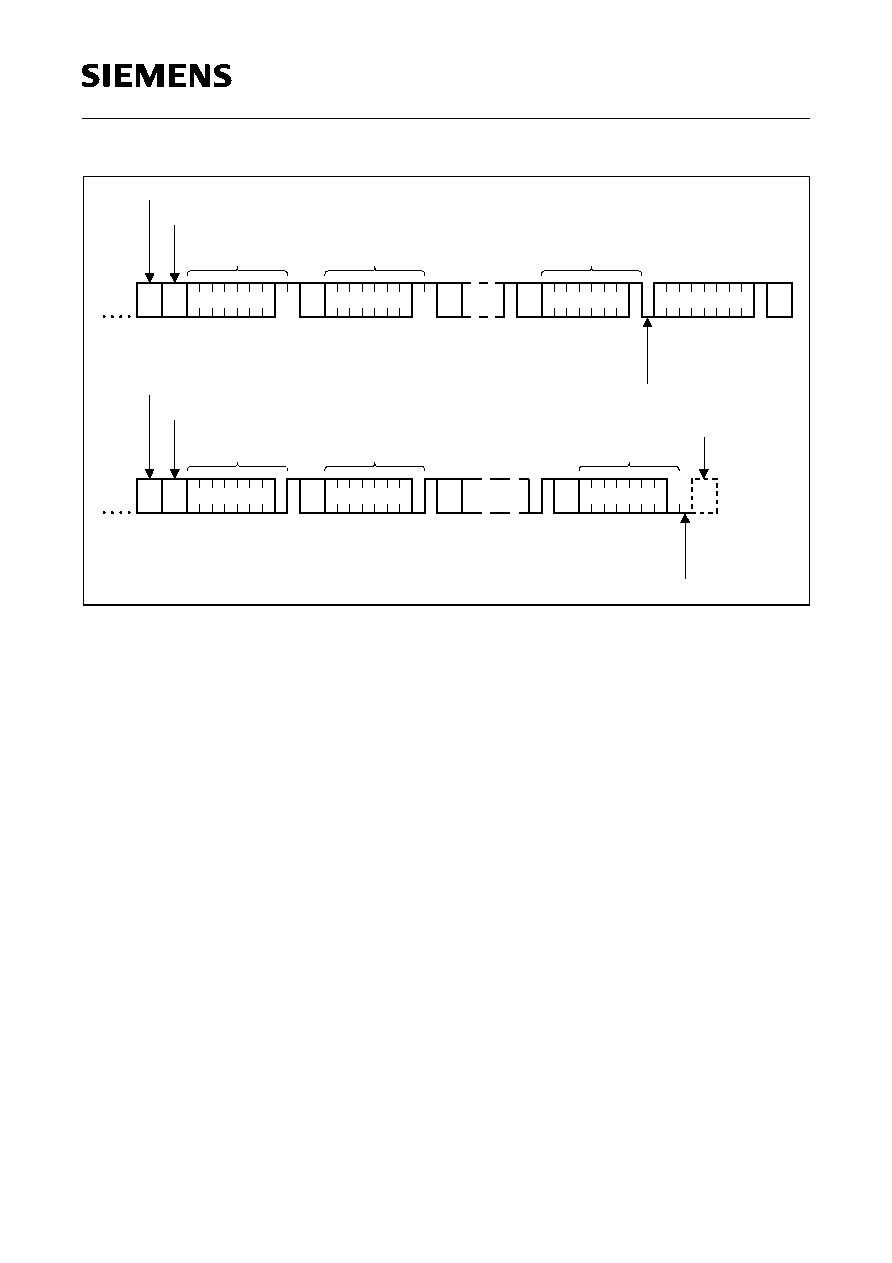
5.2
Page Write
Those bytes of the page that have not been addressed are not included in the
programming.
Figure 8
Page Write Sequence
The erase/write cycle is finished latest after 8 ms. Acknowledge polling may be used for
speed enhancement in order to indicate the end of the erase/write cycle (refer to
chapter 5.3 Acknowledge Polling).
Address Setting
The page write procedure is the same as the byte write
procedure up to the first data byte. In a page write instruction
however, entry of the EEPROM address byte EEA is followed
by a sequence of one to maximum sixteen data bytes with the
new data to be programmed. These bytes are transferred to
the internal page buffer of the EEPROM.
Transmission of Data
The first entered data byte will be stored according to the
EEPROM address n given by EEA (A0 to A7) and CSW (A8).
The internal address counter is incremented automatically
after the entered data byte has been acknowledged. The next
data byte is then stored at the next higher EEPROM address.
EEPROM addresses within the same page have common
page address bits A4 through A8. Only the respective four
least significant address bits A0 through A3 are incremented,
as all data bytes to be programmed simultaneously have to be
within the same page.
Programming Cycle
The master stops data entry by applying a STOP condition,
which also starts the internally timed erase/write cycle. In the
first step, all selected bytes are erased to "1". With the next
internal step, the addressed bytes are written according to the
contents of the page buffer.
Command Byte
CSW
S
P
C
K
A
S
T
A
R
T
T
P
O
S
EEPROM Address
EEA n
Data Byte n
Data Byte n+1
Data Byte n+15
Bus Activity
Master
SDA Line
Bus Activity
EEPROM
IED02140
0
C
K
A
C
K
A
C
K
A
C
K
A

SLx 24C04/P
Semiconductor Group
13
1998-07-27
5.3
Acknowledge Polling
During the erase/write cycle the EEPROM will not respond to a new command byte until
the internal write procedure is completed. At the end of active programming the chip
returns to the standby mode and the last entered EEPROM byte remains addressed by
the address counter. To determine the end of the internal erase/write cycle acknowledge
polling can be initiated by the master by sending a START condition followed by a
command byte CSR or CSW (read with b0 = 1 or write with b0 = 0). If the internal erase/
write cycle is not completed, the device will not acknowledge the transmission. If the
internal erase/write cycle is completed, the device acknowledges the received command
byte and the protocol activities can continue.
Figure 9
Flow Chart "Acknowledge Polling"
Internal Programming
Procedure
Send Start
Send CS-Byte
from EEPROM
Acknowledge
received?
Next Operation
No
Yes
IED02131
SLx 24C04/P
Semiconductor Group
14
1998-07-27
Figure 10
Principle of Acknowledge Polling
CSR
S
SDA
IED02166
1
P
S
1
S
CSR
S
1
P
CSR
STOP from Master initiates erase/write cycle
START from Master
Acknowledge of EEPROM
indicates complete erase/
write cycle
P
S
CSW
SDA
0
S
CSW
0
S
S
0
P
CSW
e.g. STOP condition
STOP from Master initiates erase/write cycle
START from Master
indicates complete erase/
Acknowledge of EEPROM
write cycle
SLx 24C04/P
Semiconductor Group
15
1998-07-27
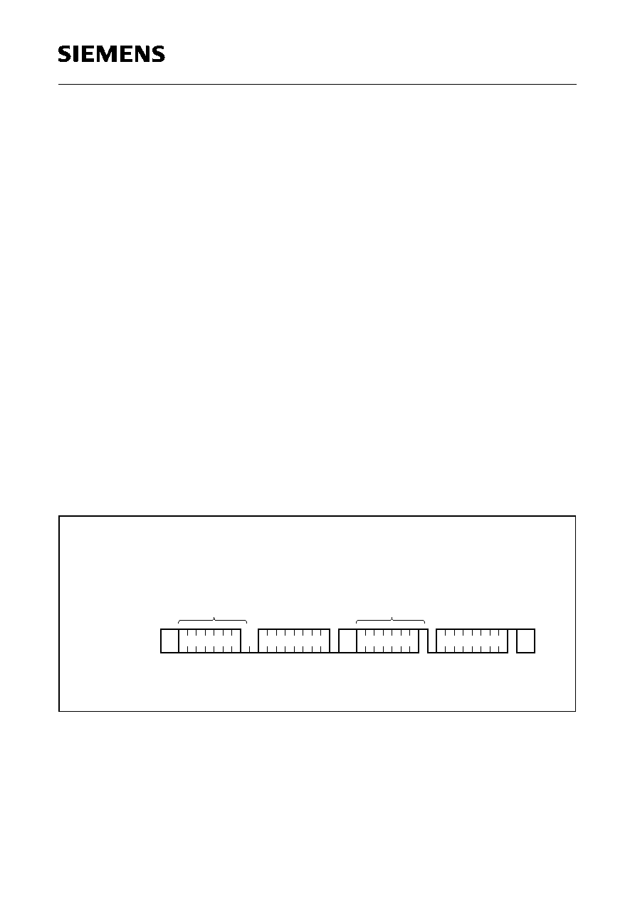
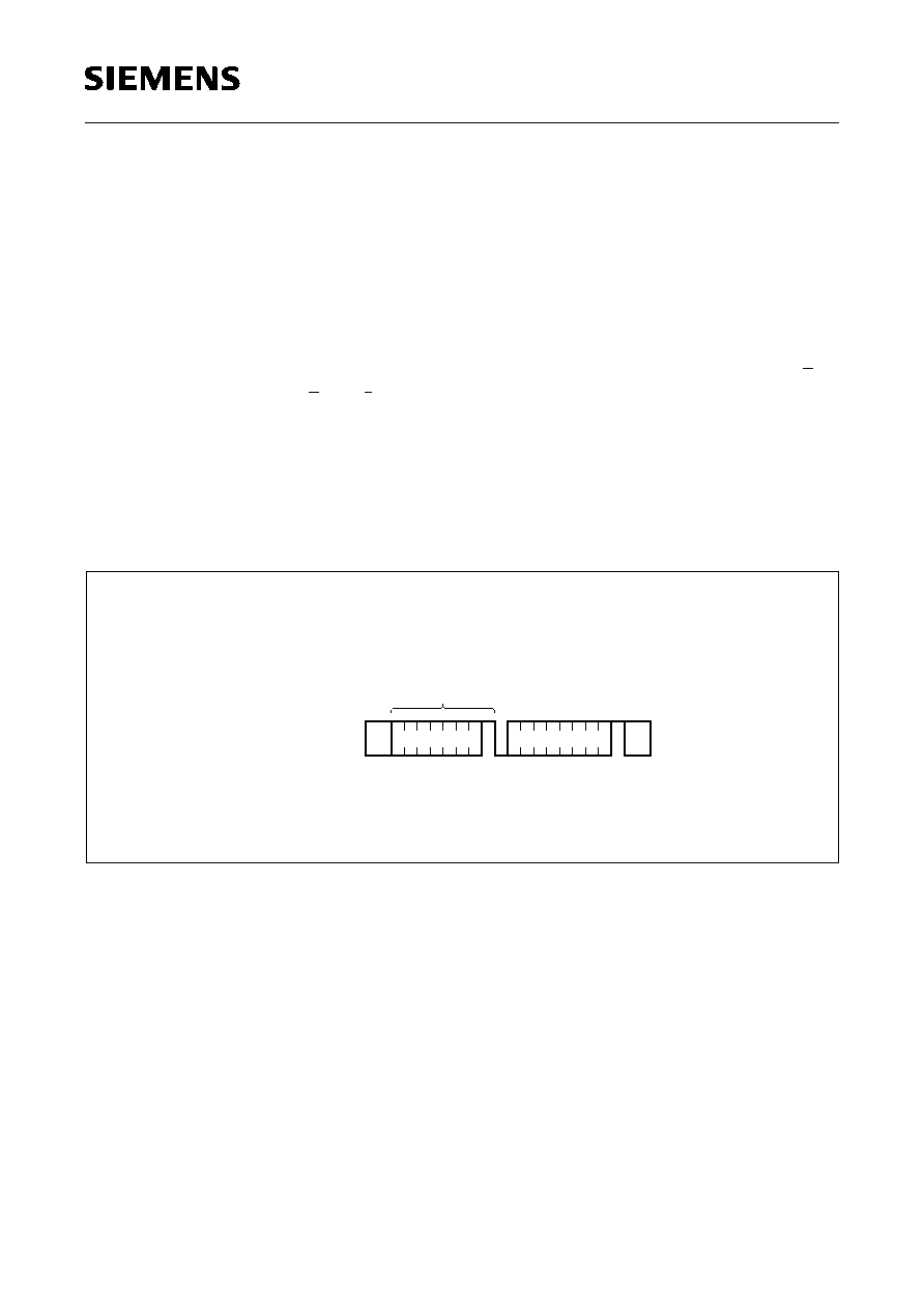
6
Read Operations
Reading of the EEPROM data is initiated by the Master with the command byte CSR.
6.1
Random Read
Random read operations allow the master to access any memory location.
Figure 11
Random Read
Address Setting
The master generates a START condition followed by the
command byte CSW. The receipt of the CSW-byte is
acknowledged by the EEPROM with a low on the SDA line.
Now the master transmits the EEPROM address (EEA) to the
EEPROM and the internal address counter is loaded with the
desired address.
Transmission of CSR
After the acknowledge for the EEPROM address is received,
the master generates a START condition, which terminates
the initiated write operation. Then the master transmits the
command byte CSR for read, which is acknowledged by the
EEPROM.
Transmission of
EEPROM Data
During the next eight clock pulses the EEPROM transmits the
data byte and increments the internal address counter.
STOP Condition from
Master
During the following clock cycle the masters releases the bus
and then transmits the STOP condition.
Command Byte
CSW
S
P
A
C
K
C
K
A
S
T
A
R
T
T
P
O
S
EEPROM Address
EEA n
Bus Activity
Master
SDA Line
Bus Activity
EEPROM
IED02133
C
K
A
Data Byte
1
0
S
T
R
A
T
S
CSR
Command Byte
SLx 24C04/P
Semiconductor Group
16
1998-07-27
6.2
Current Address Read
The EEPROM content is read without setting an EEPROM address, in this case the
current content of the address counter will be used (e.g. to continue a previous read
operation after the Master has served an interrupt).
Figure 12
Current Address Read
Transmission of CSR
For a current address read the master generates a START
condition, which is followed by the command byte CSR (chip
select read). The receipt of the CSR-byte is acknowledged by
the EEPROM with a low on the SDA line.
Transmission of
EEPROM Data
During the next eight clock pulses the EEPROM transmits the
data byte and increments the internal address counter.
STOP Condition from
Master
During the following clock cycle the masters releases the bus
and then transmits the STOP condition.
Command Byte
CSR
S
P
A
C
K
S
T
A
R
T
T
P
O
S
Bus Activity
Master
SDA Line
Bus Activity
EEPROM
IED02132
Data Byte
1

SLx 24C04/P
Semiconductor Group
17
1998-07-27
6.3
Sequential Read
A sequential read is initiated in the same way as a current read or a random read except
that the master acknowledges the data byte transmitted by the EEPROM. The EEPROM
then continues the data transmission. The internal address counter is incremented by
one during each data byte transmission.
A sequential read allows the entire memory to be read during one read operation. After
the highest addressable memory location is reached, the internal address pointer "rolls
over" to the address 0 and the sequential read continues.
The transmission is terminated by the master by releasing the SDA line (no
acknowledge) and generating a STOP condition (see figure 13).
Figure 13
Sequential Read
Data Byte n
EEPROM
Bus Activity
SDA Line
Master
Bus Activity
S
R
T
A
T
S
CSW
Command Byte
1
C
K
A
C
K
A
Data Byte n+x
Data Byte n+1
A
K
C
C
K
A
P
IED02134
S
O
P
T
SLx 24C04/P
Semiconductor Group
18
1998-07-27
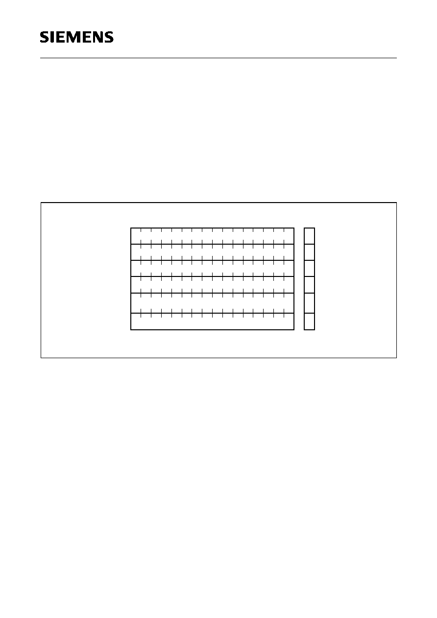
7
Page Protection Mode
TM
Each page (16 bytes) in the Data Memory can be protected against unintended data
changes by an associated protection bit. The protection bit memory consists of an
additional EEPROM of 32 bits (figure 14).
Data in the Data Memory can be modified only if the assigned protection bit is erased
(logical state "1"). After writing the data bytes to a page, the protection is achieved by
writing the associated protection bit (logical state "0"). Further changes in the data in a
protected page is possible only after erasing the protection bit.
Figure 14
Data Page and Assigned Protection Memory
A special procedure to write or erase a protection bit guarantees proper activation or
deactivation respectively of page protection. For protection bit write or erase, all 16 data
bytes of the respective page have to be entered for a second time. The data then are
compared internally with the data to be protected, and in case of identity the protection
bit is written or erased respectively.
1
0
2 3
.
.
.
.
.
.
0
1
2
3
n
Page 0
Page 1
Page 2
Page 3
Page n
Byte
Bit
Data Memory Area
Protection Bit Memory Area
IED02272
15
. . .
.
.
.
SLx 24C04/P
Semiconductor Group
19
1998-07-27
7.1
Protection Bit Handling
The bits of the protection memory can be addressed directly for reading or programming.
A protection bit address corresponds to the lowest address within the respective page
(A4 to A8, A0 to A3 = zero). The status of each protection bit is sensed internally. A
written state ("0") prevents programming in the associated page. If an already protected
memory page is accidentally addressed for programming, the programming procedure
is suppressed.
The conventional
I
2
C-Bus protocol allows data bytes to be read and programmed only.
Therefore an independent instruction sequence for addressing and manipulation of
protection bits is implemented. For protection bit instructions, the command byte CSW
with its preceding START condition followed by the associated control byte has to be
entered twice (figures 15 through 17). The first command byte CSW (with A8) is
followed by the control byte EEA with the bit/page address A0 through A3 always at zero.
The second CSW is required for entering a control byte CTx for protection bit
manipulation. The three control bytes for read, write or erase of a protection bit are listed
below (table 3):
Table 3
Control Byte for Protection Bit Manipulation
Address
Name
Definition
Function
b7
b6
b5
b4
b3
b2
b1
b0
CTR
x
x
x
x
x
x
0
0
Protection bit read
CTW
x
x
x
x
x
x
0
1
Protection bit write
CTE
x
x
x
x
x
x
1
1
Protection bit erase
SLx 24C04/P
Semiconductor Group
20
1998-07-27
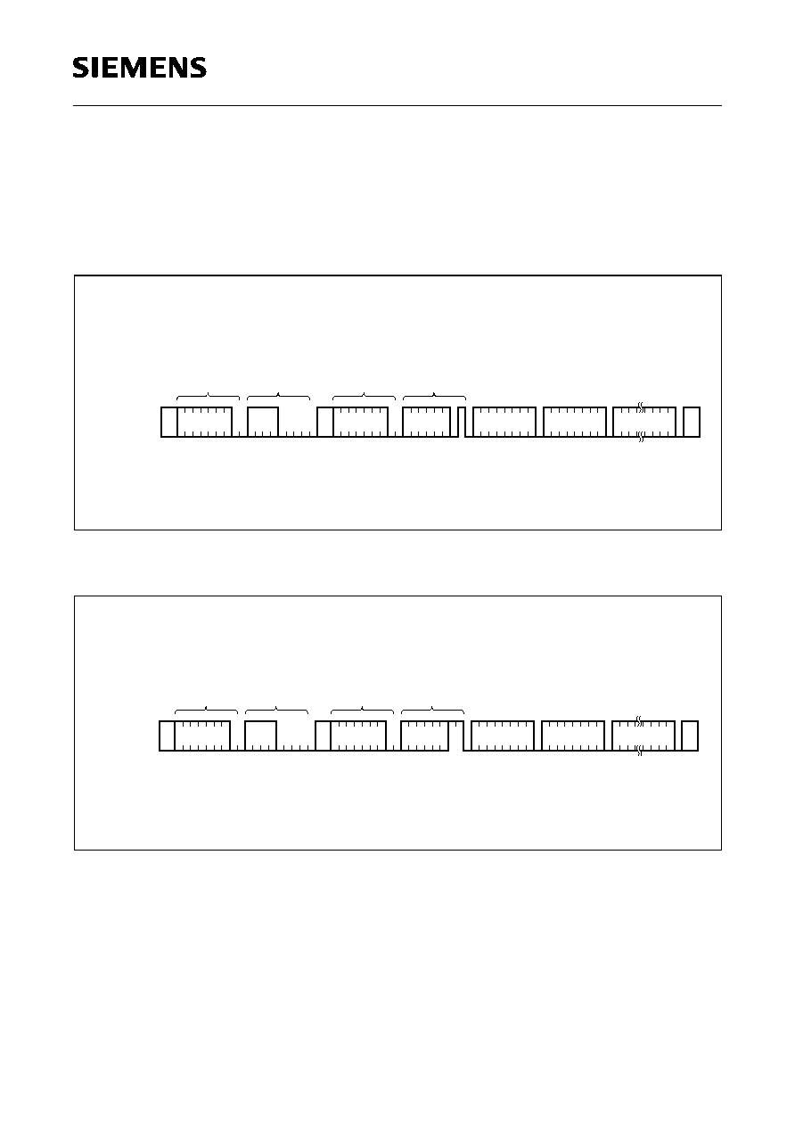
7.2
Protection Bit Write and Erase
For writing or erasing a protection bit, the data of the respective page have to be known
by the master. The data of the page are not affected by the write or erase procedure of
the protection bit. The
I
2
C-Bus protocol is shown in figure 15 for protection bit write and
figure 16 for protection bit erase.
Figure 15
Sequence for Protection Bit Write
Figure 16
Sequence for Protection Bit Erase
The first command byte CSW followed by the control byte EEA addresses the page to
be protected. The second command byte CSW (identical content of first CSW) is
followed by the control byte CTW = 01
H
for protection bit write or CTE = 03
H
for protection
bit erase. Depending on CTx, the addressed protection bit will be either written or
erased.
P
T
P
O
S
Bus Activity
Master
SDA Line
Bus Activity
EEPROM
IED02273
S
R
T
A
T
S
Command
Byte
CSW
EEPROM
Address
EEA n
Byte n
Data
Byte n+1
Data
Byte n+15
Data
C
K
A
1
0
0
0
0
0
0
0
...
C
K
A
C
K
A
C
K
A
C
K
A
C
K
A
C
K
A
R
T
A
T
S
S
Command
Byte
CSW
Control
Byte
CTW
P
T
P
O
S
Bus Activity
Master
SDA Line
Bus Activity
EEPROM
IED02274
S
R
T
A
T
S
Command
Byte
CSW
EEPROM
Address
EEA n
Byte n
Data
Byte n+1
Data
Byte n+15
Data
C
K
A
1
1
0
0
0
0
0
0
...
C
K
A
C
K
A
C
K
A
C
K
A
C
K
A
C
K
A
R
T
A
T
S
S
Command
Byte
CSW
Control
Byte
CTE

SLx 24C04/P
Semiconductor Group
21
1998-07-27
The control byte CTx is followed by 16 parameter bytes identical to the 16 data bytes of
the page to be protected or unprotected. The data of the first entered byte must be
identical to the data byte stored at the lowest address of the current page. The other 15
bytes have to be identical to the bytes stored in ascending address order within the same
page.
A successful verification of each byte is indicated by the EEPROM by pulling the SDA
line to low (acknowledge ACK).
After verification of the last byte, the bit programming procedure is initiated by the STOP
condition. Programming is started only if all 128 bits of a page have been verified
successfully. If bit programming has taken place, the address counter points to the
uppermost address of the respective page. The write or erase cycle is finished latest
after 4 ms. Acknowledge polling may be used for speed enhancement in order to
indicate the end of the write or erase cycle (refer to chapter 5.3 Acknowledge Polling).
SLx 24C04/P
Semiconductor Group
22
1998-07-27
7.3
Protection Bit Read
The byte sequence for random bit read is shown in figure 17.
Figure 17
Byte Sequence for Protection Bit Read
The first command byte CSW followed by the control byte EEA addresses the protection
bit to be read. The second command byte CSW is followed by the control byte 00
H
for
protection bit read. The first bit (MSB) of the transferred byte is the protection bit of the
addressed page. The other 7 bits are not valid. The page protection status is indicated
as following
Protection Bit = 1: A normal write operation changes the data in the associated page
Protection Bit = 0: The data in the associated page are protected against changes.
If the master acknowledges a byte with a low state of the SDA line, the protection bit of
the next page can be read as the first bit of the following byte. If the master releases the
SDA line, a STOP condition has to complete the read procedure. Any number of bytes
with a page protection status at the first bit position can be requested by the master. If
the bit of the uppermost page has been addressed, the counter has its overflow to the
lowest address according to the first page.
0
SDA Line
EEPROM
Bus Activity
Master
Bus Activity
EEA n
Address
EEPROM
CSW
Byte
Command
S
R
T
A
T
0
S
S
0
0 0 0
C
K
A
R
T
A
T
CSW
Byte
Command
S
Data
Byte n
0
C
K
A
CTR
Control
Byte
0
C
K
A
Data
Byte n+1
C
K
A
C
K
A
...
IED02139
P
C
K
A
O
P
T
S
b
b
b
K
C
A
b = Protection Bit
SLx 24C04/P
Semiconductor Group
23
1998-07-27
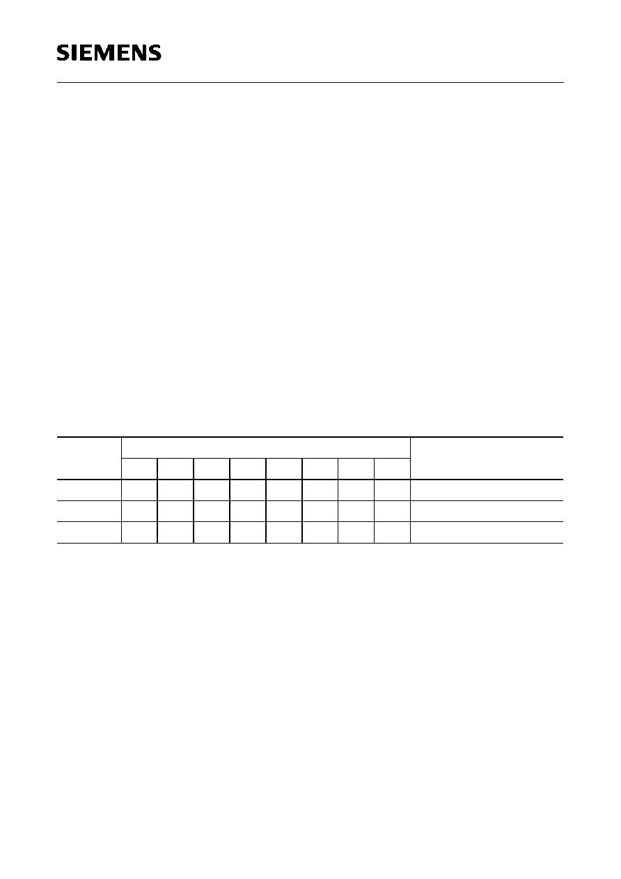
8
Electrical Characteristics
The listed characteristics are ensured over the operating range of the integrated circuit.
Typical characteristics specify mean values expected over the production spread. If not
otherwise specified, typical characteristics apply at
T
A
= 25
∞
C and the given supply
voltage.
8.1
Absolute Maximum Ratings
Stresses above those listed here may cause permanent damage to the device. This is a
stress rating only and functional operation of the device at these or any other conditions
above those indicated in the operational section of this data sheet is not implied.
Exposure to absolute maximum ratings for extended periods may affect device reliability.
Parameter
Limit Values
Units
Operating temperature
range 1 (industrial)
range 2 (automotive)
≠ 40 to + 85
≠ 40 to + 125
∞C
∞C
Storage temperature
≠ 65 to + 150
∞C
Supply voltage
≠ 0.3 to + 7.0
V
All inputs and outputs with respect to ground
≠ 0.3 to
V
CC
+ 0.5
V
ESD protection (human body model)
4000
V
8.2
DC Characteristics
Parameter
Symbol
Limit Values
Units Test Condition
min.
typ. max.
Supply voltage
V
CC
4.5
5.5
V
5 V type
V
CC
2.7
5.5
V
3 V type
Supply current
1)
(write)
I
CC
1
3
mA
V
CC
= 5 V;
f
c
= 100 kHz
Standby
current
2)
I
SB
50
µ
A
Inputs at
V
CC
or
V
SS
Input leakage
current
I
LI
0.1
10
µ
A
V
IN
=
V
CC
or
V
SS
Output leakage
current
I
LO
0.1
10
µ
A
V
OUT
=
V
CC
or
V
SS
Input low
voltage
V
IL
≠ 0.3
0.3
◊
V
CC
V
SLx 24C04/P
Semiconductor Group
24
1998-07-27
1)
The values for
I
CC
are maximum peak values
2)
Valid over the whole temperature range
3)
This parameter is characterized only
Input high
voltage
V
IH
0.7
◊
V
CC
V
CC
+ 0.5 V
Output low
voltage
V
OL
0.4
V
I
OL
= 3 mA;
V
CC
= 5 V
I
OL
= 2.1 mA;
V
CC
= 3 V
Input/output
capacitance
(SDA)
C
I/O
8
3)
pF
V
IN
= 0 V;
V
CC
= 5 V
Input
capacitance
(other pins)
C
IN
6
3)
pF
V
IN
= 0 V;
V
CC
= 5 V
Capacitive load
for each bus line
C
b
400
pF
8.2
DC Characteristics (cont'd)
Parameter
Symbol
Limit Values
Units Test Condition
min.
typ. max.
SLx 24C04/P
Semiconductor Group
25
1998-07-27
1)
The minimum rise and fall times can be calculated as follows: 20 + (0.1/pF)
◊
C
b
[ns]
Example:
C
b
= 100 pF
t
R
= 20 + 0.1
◊
100 [ns] = 30 ns
8.3
AC Characteristics
Parameter
Symbol
Limit Values
V
CC
= 2.7-5.5 V
Limit Values
V
CC
= 4.5-5.5 V
Units
min.
max.
min.
max.
SCL clock frequency
f
SCL
100
400
kHz
Clock pulse width low
t
low
4.7
1.2
µ
s
Clock pulse width high
t
high
4.0
0.6
µ
s
SDA and SCL rise time
t
R
1000
1)
300
ns
SDA and SCL fall time
t
F
300
1)
300
ns
Start set-up time
t
SU.STA
4.7
0.6
µ
s
Start hold time
t
HD.STA
4.0
0.6
µ
s
Data in set-up time
t
SU.DAT
200
100
ns
Data in hold time
t
HD.DAT
0
0
µ
s
SCL low to SDA data out valid
t
AA
0.1
4.5
0.1
0.9
µ
s
Data out hold time
t
DH
100
50
ns
Stop set-up time
t
SU.STO
4.0
0.6
µ
s
Time the bus must be free before
a new transmission can start
t
BUF
4.7
1.2
µ
s
SDA and SCL spike suppression
time at constant inputs
t
l
50
100
50
100
ns
8.4
Erase and Write Characteristics
Parameter
Symbol
Limit Values
V
CC
= 2.7-5.5 V
Limit Values
V
CC
= 4.5-5.5 V
Units
typ.
max.
typ.
max.
Erase + write cycle (per page)
t
WR
5
8
5
8
ms
Erase page protection bit
2.5
4
2.5
4
ms
Write page protection bit
2.5
4
2.5
4
ms
SLx 24C04/P
Semiconductor Group
26
1998-07-27
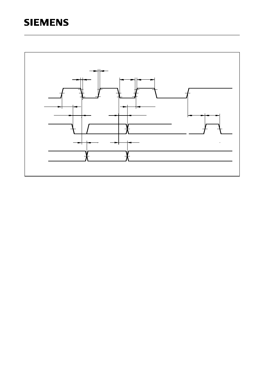
Figure 18
Bus Timing Data
t
F
R
t
HD.STA
t
SU.STA
t
LOW
t
HD.DAT
t
t
SU.DAT
t
HIGH
t
SU.STO
BUF
t
DH
t
t
AA
IED02127
SCL
SDA In
SDA Out
Start Condition
Stop Condition
SLx 24C04/P
Semiconductor Group
27
1998-07-27
9
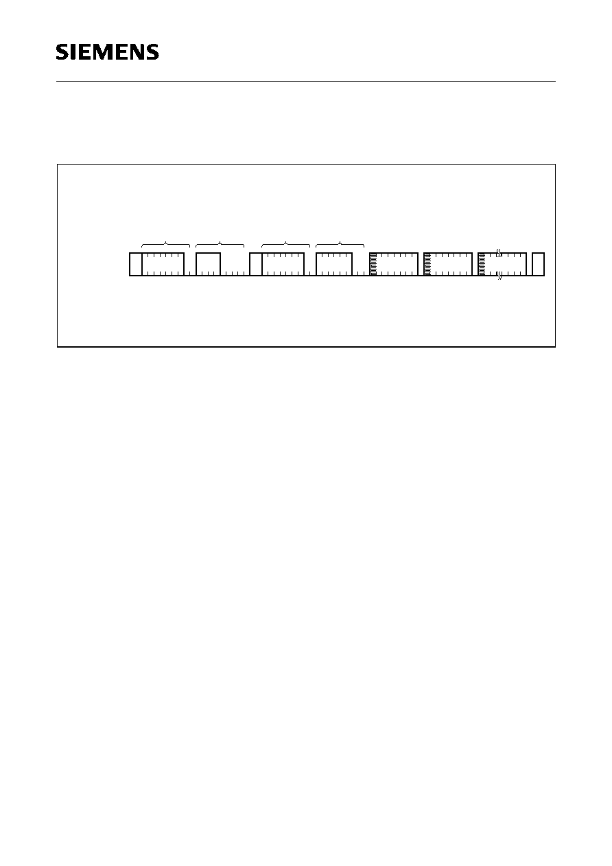
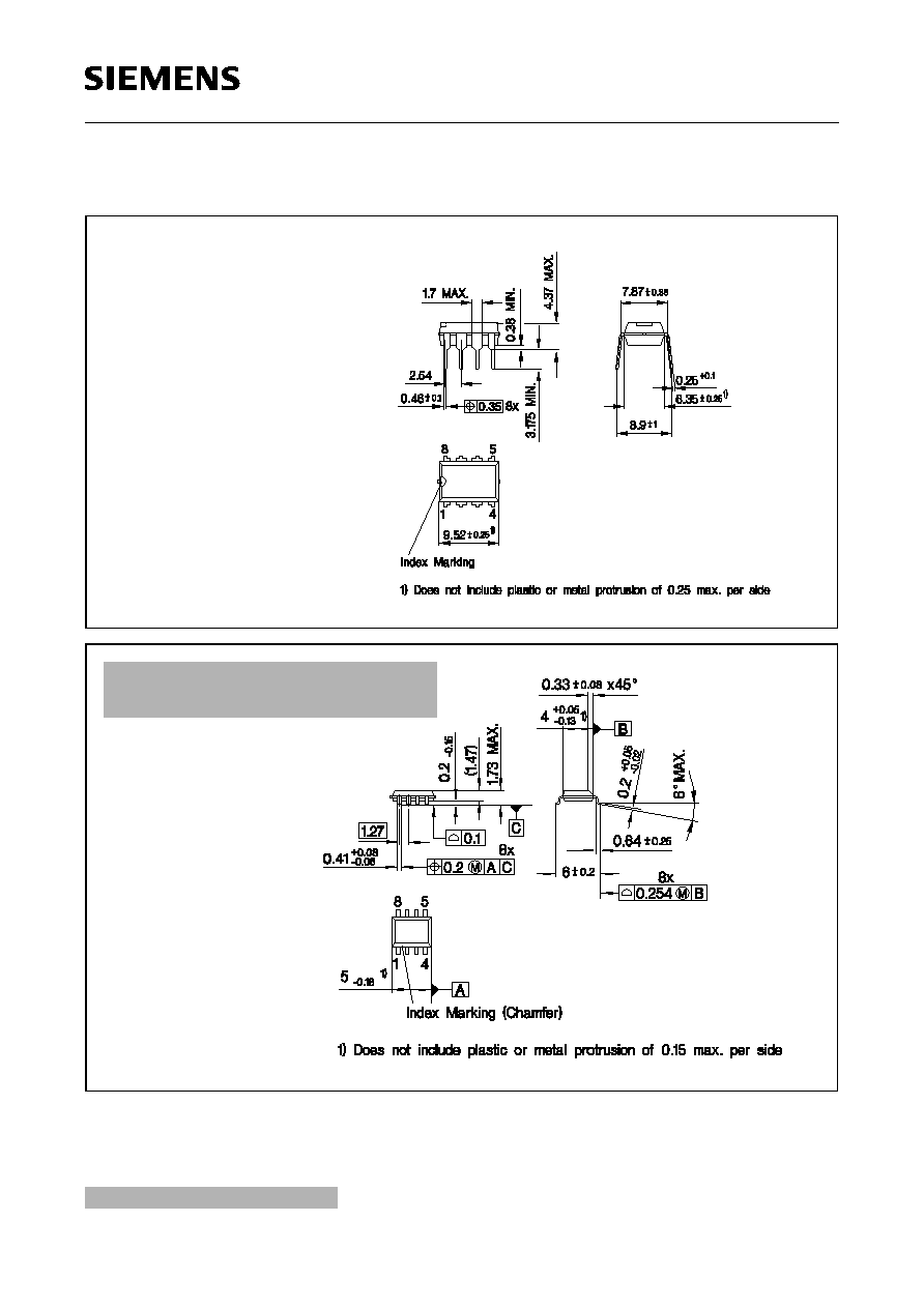
Package Outlines
Sorts of Packing
Package outlines for tubes, trays etc. are contained in our
Data Book "Package Information".
SMD = Surface Mounted Device
Dimensions in mm
GPD
0
558
3
P-DIP-8-4
(Plastic Dual In-line Package)
G
PS0
903
2
P-DSO-8-3
(Plastic Dual Small Outline Package)