
ICs for Consumer Electronics
VPS / PDC-plus Decoder
SDA 5650/X
Data Sheet 02.97

Edition 02.97
This edition was realized using the software system FrameMaker
Æ
.
Published by Siemens AG,
Bereich Halbleiter, Marketing-
Kommunikation, Balanstraþe 73,
81541 M¸nchen
©
Siemens AG 1997.
All Rights Reserved.
Attention please!
As far as patents or other rights of third parties are concerned, liability is only assumed for components, not for applications, processes
and circuits implemented within components or assemblies.
The information describes the type of component and shall not be considered as assured characteristics.
Terms of delivery and rights to change design reserved.
For questions on technology, delivery and prices please contact the Semiconductor Group Offices in Germany or the Siemens Companies
and Representatives worldwide (see address list).
Due to technical requirements components may contain dangerous substances. For information on the types in question please contact
your nearest Siemens Office, Semiconductor Group.
Siemens AG is an approved CECC manufacturer.
Packing
Please use the recycling operators known to you. We can also help you ≠ get in touch with your nearest sales office. By agreement we
will take packing material back, if it is sorted. You must bear the costs of transport.
For packing material that is returned to us unsorted or which we are not obliged to accept, we shall have to invoice you for any costs in-
curred.
Components used in life-support devices or systems must be expressly authorized for such purpose!
Critical components1 of the Semiconductor Group of Siemens AG, may only be used in life-support devices or systems2 with the express
written approval of the Semiconductor Group of Siemens AG.
1 A critical component is a component used in a life-support device or system whose failure can reasonably be expected to cause the
failure of that life-support device or system, or to affect its safety or effectiveness of that device or system.
2 Life support devices or systems are intended (a) to be implanted in the human body, or (b) to support and/or maintain and sustain hu-
man life. If they fail, it is reasonable to assume that the health of the user may be endangered.
SDA 5650/X
Revision History:
Current Version: 02.97
Previous Version:
Page
(in previous
Version)
Page
(in current
Version)
Subjects (major changes since last revision)

SDA 5650/X
Table of Contents
Page
Semiconductor Group
3
02.97
1
General Description . . . . . . . . . . . . . . . . . . . . . . . . . . . . . . . . . . . . . . . . . . . 4
1.1
Features . . . . . . . . . . . . . . . . . . . . . . . . . . . . . . . . . . . . . . . . . . . . . . . . . . . . . 4
1.2
Pin Configurations . . . . . . . . . . . . . . . . . . . . . . . . . . . . . . . . . . . . . . . . . . . . . 5
1.3
Pin Description . . . . . . . . . . . . . . . . . . . . . . . . . . . . . . . . . . . . . . . . . . . . . . . . 6
2
System Description . . . . . . . . . . . . . . . . . . . . . . . . . . . . . . . . . . . . . . . . . . . 8
2.1
Functions . . . . . . . . . . . . . . . . . . . . . . . . . . . . . . . . . . . . . . . . . . . . . . . . . . . . 8
2.2
I
2
C Bus . . . . . . . . . . . . . . . . . . . . . . . . . . . . . . . . . . . . . . . . . . . . . . . . . . . . . . 9
2.2.1
General Information . . . . . . . . . . . . . . . . . . . . . . . . . . . . . . . . . . . . . . . . . . . . 9
2.2.2
Chip Address . . . . . . . . . . . . . . . . . . . . . . . . . . . . . . . . . . . . . . . . . . . . . . . . 10
2.2.3
Write Mode . . . . . . . . . . . . . . . . . . . . . . . . . . . . . . . . . . . . . . . . . . . . . . . . . . 10
2.2.4
Read Mode . . . . . . . . . . . . . . . . . . . . . . . . . . . . . . . . . . . . . . . . . . . . . . . . . . 12
2.3
Order of Data Output on the
I
2
C Bus and Bit Allocation
of PDC/VPS Operating Modes . . . . . . . . . . . . . . . . . . . . . . . . . . . . . . . . . . . 13
2.4
Order of Data Output on the
I
2
C Bus and Bit Allocation
for the Header Time Mode (MAB=0) . . . . . . . . . . . . . . . . . . . . . . . . . . . . . . 17
2.5
Description of DAVN and EHB Outputs . . . . . . . . . . . . . . . . . . . . . . . . . . . . 25
3
Electrical Characteristics . . . . . . . . . . . . . . . . . . . . . . . . . . . . . . . . . . . . . 26
4
PDC/VPS-Receiver . . . . . . . . . . . . . . . . . . . . . . . . . . . . . . . . . . . . . . . . . . . 30
5
Appendix . . . . . . . . . . . . . . . . . . . . . . . . . . . . . . . . . . . . . . . . . . . . . . . . . . . 31
5.1
Control Register Write (
I
2
C-Bus Write) . . . . . . . . . . . . . . . . . . . . . . . . . . . . 31
5.2
Data Register Read (
I
2
C-Bus Read) . . . . . . . . . . . . . . . . . . . . . . . . . . . . . . 31
5.3
DAVN and EHB Timing . . . . . . . . . . . . . . . . . . . . . . . . . . . . . . . . . . . . . . . . 32
5.4
Position of Teletext and VPS Data Lines within
the Vertical Blanking Interval . . . . . . . . . . . . . . . . . . . . . . . . . . . . . . . . . . . . 33
5.5
Definition of Voltage Levels for VPS Data Line . . . . . . . . . . . . . . . . . . . . . . 33
5.6
BDSP 8/30 Format 1 Bit Allocation . . . . . . . . . . . . . . . . . . . . . . . . . . . . . . . 34
5.7
Structure of the Teletext Data Packet 8/30 Format 2 . . . . . . . . . . . . . . . . . . 35
5.8
BDSP 8/30 Format 2 Bit Allocation . . . . . . . . . . . . . . . . . . . . . . . . . . . . . . . 35
5.9
Data Format of Programme Delivery Data in the Dedicated TV Line (VPS) 38
6
Package Outlines . . . . . . . . . . . . . . . . . . . . . . . . . . . . . . . . . . . . . . . . . . . . 40
Purchase of Siemens
I
2
C components conveys the license under the Philips
I
2
C patent to use the components
in the
I
2
C system provided the system conforms to the
I
2
C specifications defined by Philips.
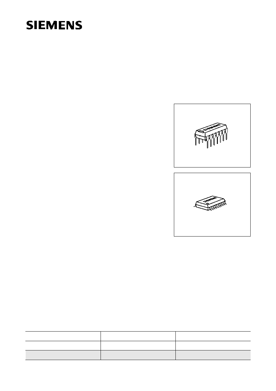
P-DIP-14-1
P-DSO-20-1
VPS / PDC-plus Decoder
SDA 5650/X
Semiconductor Group
4
02.97
CMOS
Type
Ordering Code
Package
SDA 5650
Q67100-H5164
P-DIP-14-1
SDA 5650X
Q67106-H5163
P-DSO-20-1 (SMD)
1
General Description
The PDC plus SDA 5650 decoder chip receives all
VPS and 8/30 Format 1 and 2 data together with the
teletext header information for easy identification of
broadcast transmitter. The SDA 5650 includes a
storage capacity of 16 bytes which can be used in
different ways depending on selected modes.
1.1
Features
∑ Single chip receiver for PDC data for
Broadcast Data Service Packet (BDSP 8/30/2
according to CCIR teletext system B.)
VPS Data in dedicated line no. 16 of the vertical
blanking interval (VBI)
∑ Reception of BDSP packet 8/30/1
Unified Date and Time (UDT)
Network indentification code (NIC)
Short program label (SPL)
∑ Reception of teletext header row
Bytes no. 14 - 45 containing date, clock time and identification
∑ On chip data slicer
∑ Low external component count
∑
I
2
C-Bus interface
Communication with external microcontroller
∑ PDC/VPS operation mode selectable via
I
2
C-Bus register
∑ Pin and software compatible to PDC/VPS decoder SDA 5649
∑ 5 V supply voltage
∑ Video input signal level: 0.7 Vpp to 2.0 Vpp
∑ Technology: CMOS
∑ P-DIP-14-1 and P-DSO-20-1 package
SDA 5650/X
Semiconductor Group
5
02.97
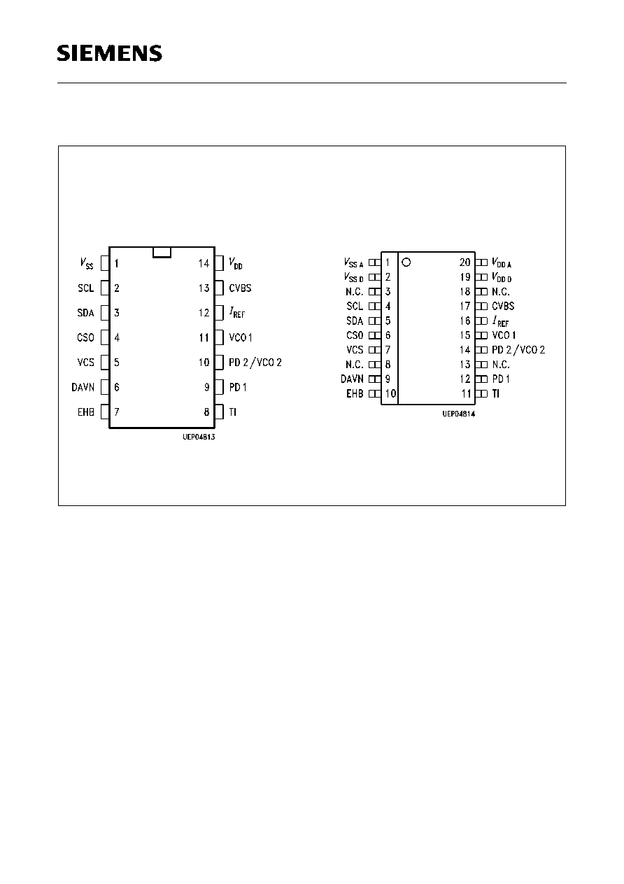
1.2
Pin Configurations
Figure 1
P-DIP-14-1
P-DSO-20-1
SDA 5650/X
Semiconductor Group
6
02.97
1.3
Pin Description
Pin No.
Symbol Function
P-DIP-14-1 P-DSO-20-1
1
V
SS
Ground (0 V)
1
V
SSA
Analog ground (0 V)
2
V
SSD
Digital ground (0 V)
3, 8, 13, 18 N.C.
Not connected
2
4
SCL
Serial clock input of
I
2
C Bus.
3
5
SDA
Serial data input of
I
2
C Bus.
4
6
CS0
Chip select input determining the
I
2
C-Bus addresses:
20
H
/ 21
H
, when pulled low
22
H
/ 23
H
, when pulled high.
5
7
VCS
Video Composite Sync output from sync slicer used for
PLL based clock generation.
6
9
DAVN
Data available output active low, when VPS data is
received.
7
10
EHB
Output signaling the presence of the first field active
high.
8
11
TI
Test input; activates test mode when pulled high.
Connect to ground for operating mode.
9
12
PD1
Phase detector/charge pump output of data PLL
(DAPLL).
10
14
PD2/
VCO2
Connector of the loop filter for the SYSPLL.
11
15
VCO1
Input to the voltage controlled oscillator #1 of the
DAPLL.
12
16
I
REF
Reference current input for the on-chip analog circuit.
13
17
CVBS
Composite video signal input.
14
V
DD
Positive supply voltage (+ 5 V nom.).
19
V
DDD
Positive supply voltage for the digital circuits
(+ 5 V nom.).
20
V
DDA
Positive supply voltage for the analog circuits
(+ 5 V nom.).

SDA 5650/X
Semiconductor Group
7
02.97
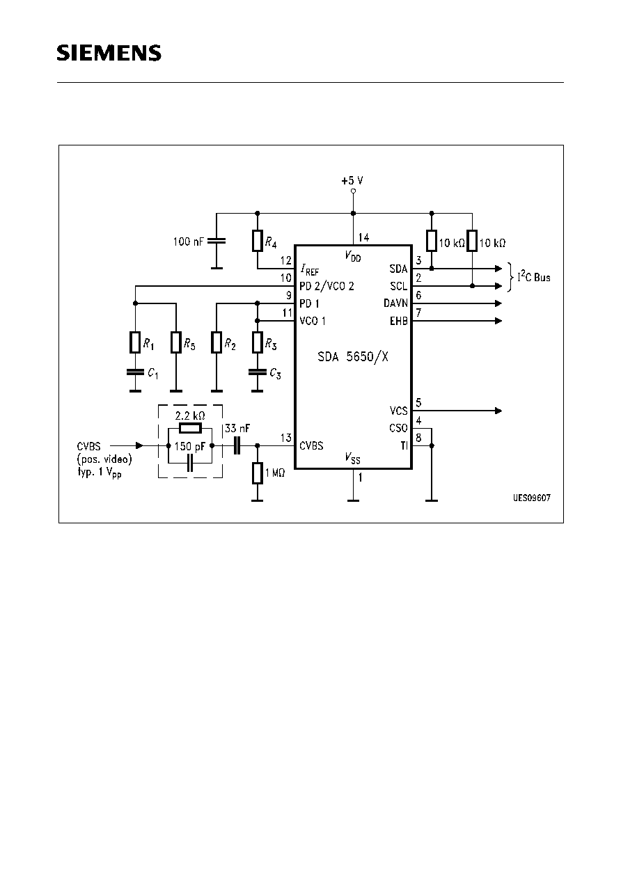
Block Diagram
Figure 2

SDA 5650/X
Semiconductor Group
8
02.97
2
System Description
2.1
Functions
Referring to the functional block diagram of the PDC / VPS decoder, the composite video
signal with negative going sync pulses is coupled to the pin CVBS through a capacitor
which is used for clamping the bottom of the sync pulses to an internally fixed level. The
signal is passed on to the slicer, an analogue circuitry separating the sync and the data
parts of the CVBS signal, thus yielding the digital composite sync signal VCS and a
digital data signal for further processing by comparing those signals to internally
generated slicing levels.
The output of the sync separator is forwarded, on one hand, to the output pin VCS, and
on the other hand, to the clock generator and the timing block. The VCS signal
represents a key signal that is used for deriving a system clock signal by means of a PLL
and all other timing signal.
The data slicer separates the data signal from the CVBS signal by comparing the video
voltage to an internally generated slicing level which is found by averaging the data
signal during TV line no. 16 in the VPS mode or by averaging the data signal during the
clock run-in period of the teletext lines during the data entry window (DEW) in PDC
mode.
The clock generator delivers the system clock needed for the basic timing as well as for
the regeneraton of the dataclock. It is based on two phase locked loops (PLL's) all parts
of which are integrated on chip with the exception of the loop filter components. Each of
the PLL's is composed of a voltage controlled relaxation oscillator (VCO), a phase/
frequency detector (PFD), and a charge pump which converts the digital output signals
of the PFD to an analogue current. That current is transformed to a control voltage for
the VCO by the off-chip loop filter. The generated VCO frequencies are 10 MHz and
13.875 MHz for VPS mode and PDC mode, respectively.
All signals necessary for the control of sync and data slicing as well as for the data
acquisition are generated by the Timing block.
The SDA 5650 can be operated in three different modes: Depending on the selected
operating mode, either teletext lines carrying 8/30 packages, the dedicated TV line
no. 16 (VPS) or the teletext header bytes 38-45, 30-37, 22-29 and 14-21 are acquired.
In PDC mode, only teletext rows 8/30 containing Broadcast Data Service Package
(BDSP) information are acquired. The relevant bytes of 8/30 format 1 (8/30/1) and 8/30
format 2 (8/30/2) are extracted. The 8/30/1-bytes are stored in the acquisition register in
a transparent way without any bit manipulation, whereas the Hamming coded bytes of
packet 8/30/2 are Hamming-checked and bytes with one bit error are corrected. The
storage of error free or corrected 8/30/2-data bytes in the transfer register to the
I
2
C Bus
is signalled by the DAVN output going low.

SDA 5650/X
Semiconductor Group
9
02.97
In VPS mode, the extracted data bits of TV line no. 16 are checked for biphase errors.
With no biphase errors encountered, the acquired bytes are stored in the transfer
register to the
I
2
C Bus. That transfer is signalled by a H/L transition of the DAVN output,
as well.
In TTX header mode A bytes 38-45 and 30-37 are accessed in this order. This assures
software compatibility to the SDA 5649. In mode B bytes 22-29 and 14-21 are accessed
in this order.
In all three operating modes data are updated when a new data line has been received,
provided that the chip is not accessed via the
I
2
C Bus at the same time.
A micro controller can read the stored bytes via the
I
2
C-Bus interface at any time.
However, one must be aware that the storage of new data from the acquisition interface
is inhibited as long as the PDC decoder is being accessed via the
I
2
C Bus.
Note: In order to achieve maximum system performance it is recommended to start the
SDA 5650 in VPS mode (state after power on) and read the register to check
whether line 16 is received. After reception of VPS data inline 16 the SDA 5650
can be switched to 8/30 mode and waiting for packet 8/30 data. Since VPS data
in line 16 is transmitted every frame and PDC data in packet 8/30 is transmitted
nearly every second the recognition of both VPS and 8/30 packets can be done
within PDC-system constraints (about 1 sec).
2.2
I
2
C Bus
2.2.1
General Information
The
I
2
C-Bus interface implemented on the PDC decoder is a slave transmitter/receiver,
i. e., both reading from and writing to the PDC / VPS decoder is possible. The clock line
SCL is controlled only by the bus master usually being a micro controller, whereas the
SDA line is controlled either by the master or by the slave. A data transfer can only be
initiated by the bus master when the bus is free, i. e., both SDA and SCL lines are in a
high state. As a general rule for the
I
2
C Bus, the SDA line changes state only when the
SCL line is low. The only exception to that rule are the Start Condition and the Stop
Condition. Further Details are given below. The following abbreviations are used:
START:
Start Condition generated by master
AS:
Acknowledge by slave
AM:
Acknowledge by master
NAM:
No Acknowledge by master
STOP:
Stop condition generated by master
SDA 5650/X
Semiconductor Group
10
02.97
2.2.2
Chip Address
There are two pairs of chip addresses, which are selected by the CS0-input pin
according to the following table:
2.2.3
Write Mode
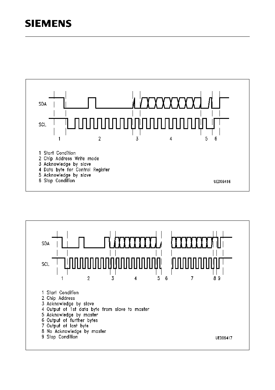
For writing to the PDC decoder, the following format has to be used:
Description of Data Transfer (Write Mode)
Step1:
In order to start a data transfer the master generates a Start Condition on the
bus by pulling the SDA line low while the SCL line is held high.
Step 2:
The bus master puts the chip address on the SDA line during the next eight
SCL pulses.
Step 3:
The master releases the SDA line during the ninth clock pulse. Thus the slave
can generate an acknowledge (AS) by pulling the SDA line to a low level.
Step 4:
The controller transmits the data byte to set the Control register
Step 5:
The slave acknowledges the reception of the byte.
Step 6:
The master concludes the data communication by generating a Stop
Condition.
The write mode is used to set the
I
2
C-Bus control register which determines the
operating mode:
CS0 Input
Write Mode
Read Mode
Low
20 (hex)
21 (hex)
High
22 (hex)
23 (hex)
Start Chipaddress and Write Mode
AS
Byte to set Control Register
AS
Stop

SDA 5650/X
Semiconductor Group
11
02.97
Control Register:
Default: All bits are set to 0 on power-up.
Bits 4 through 7 are used for test purposes and must not be changed for normal
operation by user software!
Bit 0:
determines, which kind of data is accessed via the
I
2
C Bus when PDC
mode is active:
Bit 1:
determines the operating mode:
Bit 2:
determines whether BDSP 8/30/1-data or header row data is
accessible:
Bit 3:
determines mode of teletext header access:
Bit Number: 7
6
5
4
3
2
1
0
T4
T3
T2
T1
MAB
HDT
PDC/
VPS
FOR1/
FOR2
Value
0
1
BDSP 8/ 30/ 2 data accessible
BDSP 8/ 30/ 1 or header row
data accessible (refer to description of
Bit 2)
Value
0
1
VPS mode active
PDC mode active
Value
0
1
BDSP 8/30/1 data accessible
Bytes of teletext header in mode A or B
(see Bit 3)
Value
0
1
Mode A: header bytes in order 38-45,
30-37
Mode B: header bytes in order 22-29,
14-21

SDA 5650/X
Semiconductor Group
12
02.97
2.2.4
Read Mode
For reading from the PDC decoder, the following format has to be used
The contents of up to 16 registers (bytes) can be read starting with byte 1 bit 7 (refer to
the table Order of Data Output on the
I
2
C Bus and...) depending on the selected
operating mode.
Description of Data Transfer (Read Mode)
Step1:
To start a data transfer the master generates a Start Condition on the bus by
pulling the SDA line low while the SCL line is held high. The byte address
counter in the decoder is reset and points to the first byte to be output.
Step 2:
The bus master puts the chip address on the SDA line during the next eight
SCL pulses.
Step 3:
The master releases the SDA line during the ninth clock pulse. Thus the slave
can generate an acknowledge (AS) by pulling the SDA line to a low level. At
this moment, the slave switches to transmitting mode.
Step 4:
During the next eight clock pulses the slave puts the addressed data byte
onto the SDA line.
Step 5:
The reception of the byte is acknowledged by the master device which, in
turn, pulls down the SDA line during the next SCL clock pulse. By
acknowledging a byte, the master prompts the slave to increment its internal
address counter and to provide the output of the next data byte.
Step 6:
Steps no. 4 and no. 5 are repeated, until the desired amount of bytes have
been read.
Step 7:
The last byte is output by the slave since it will not be acknowledged by the
master.
Step 8:
To conclude the read operation, the master doesn't acknowledge the last byte
to be received. A No Acknowledge by the master (NAM) causes the slave to
switch from transmitting to receiving mode. Note that the master can
prematurely cease any reading operation by not acknowledging a byte.
Step 9:
The master gains control over the SDA line and concludes the data transfer
by generating a Stop Condition on the bus, i. e., by producing a low/high
transition on the SDA line while the SCL line is in a high state. With the SDA
and the SCL lines being both in a high state, the
I
2
C Bus is free and ready for
another data transfer to be started.
Start
Chipaddress Read Mode AS 1st Byte AM ..... Last Byte NAM
Stop

SDA 5650/X
Semiconductor Group
13
02.97
2.3
Order of Data Output on the
I
2
C Bus and Bit Allocation of PDC/VPS
Operating Modes
I
2
C Bus
PDC Packet 8/30
VPS Mode
Format 1
Format 2
Byte 1
bit 7
6
5
4
3
2
1
0
byte 15
bit 0
2)
1
2
3
4
5
6
7
byte 16
bit 0
1)
1
2
3
byte 17
bit 0
1
2
3
byte 11
bit 0
2)
1
2
3
4
5
6
7
Byte 2
bit 7
6
5
4
3
2
1
0
byte 16
bit 0
1
2
3
4
5
6
7
byte 18
bit 0
1
2
3
byte 19
bit 0
1
2
3
byte 12
bit 0
1
2
3
4
5
6
7
Byte 3
bit 7
6
5
4
3
2
1
0
byte 17
bit 0
1
2
3
4
5
6
7
byte 20
bit 0
1
2
3
byte 21
bit 0
1
2
3
byte 13
bit 0
1
2
3
4
5
6
7
Byte 4
bit 7
6
5
4
3
2
1
0
byte 18
bit 0
1
2
3
4
5
6
7
byte 22
bit 0
1
2
3
byte 23
bit 0
1
2
3
byte 14
bit 0
1
2
3
4
5
6
7
1) Message bit numbers according to EBU specification of PDC system.
2) Transmission bit number.
t

SDA 5650/X
Semiconductor Group
14
02.97
Byte 5
bit 7
6
5
4
3
2
1
0
byte 19
bit 0
1
2
3
4
5
6
7
byte 14
bit 0
1
2
3
byte 15
bit 0
1
2
3
byte 5
bit 0
1
2
3
4
5
6
7
Byte 6
bit 7
6
5
4
3
2
1
0
byte 20
bit 0
1
2
3
4
5
6
7
byte 24
bit 0
1
2
3
byte 25
bit 0
1
2
3
byte 15
bit 0
1
2
3
4
5
6
7
Byte 7
bit 7
6
5
4
3
2
1
0
byte 21
bit 0
1
2
3
4
5
6
7
byte 13
bit 0
1
2
3
≠ set to "1"
≠ set to "1"
≠ set to "1"
≠ set to "1"
≠ set to "1"
≠ set to "1"
≠ set to "1"
≠ set to "1"
≠ set to "1"
≠ set to "1"
≠ set to "1"
≠ set to "1"
Byte 8
bit 7
6
5
4
3
2
1
0
byte 13
bit 0
1
2
3
4
5
6
7
1) Message bit numbers according to EBU specification of PDC system.
2) Transmission bit number.
2.3
Order of Data Output on the
I
2
C Bus and Bit Allocation of PDC/VPS
Operating Modes (cont'd)
I
2
C Bus
PDC Packet 8/30
VPS Mode
Format 1
Format 2

SDA 5650/X
Semiconductor Group
15
02.97
Byte 9
bit 7
6
5
4
3
2
1
0
byte 14
bit 0
1
2
3
4
5
6
7
Byte 10
bit 7
6
5
4
3
2
1
0
byte 22
bit 0
1
2
3
4
5
6
7
Byte 11
bit 7
6
5
4
3
2
1
0
byte 23
bit 0
1
2
3
4
5
6
7
1) Message bit numbers according to EBU specification of PDC system.
2) Transmission bit number.
2.3
Order of Data Output on the
I
2
C Bus and Bit Allocation of PDC/VPS
Operating Modes (cont'd)
I
2
C Bus
PDC Packet 8/30
VPS Mode
Format 1
Format 2

SDA 5650/X
Semiconductor Group
16
02.97
Byte 12
bit 7
6
5
4
3
2
1
0
byte 24
bit 0
1
2
3
4
5
6
7
Byte 13 bit7
6
5
4
3
2
1
0
byte 25
bit 0
1
2
3
4
5
6
7
1) Message bit numbers according to EBU specification of PDC system.
2) Transmission bit number.
2.3
Order of Data Output on the
I
2
C Bus and Bit Allocation of PDC/VPS
Operating Modes (cont'd)
I
2
C Bus
PDC Packet 8/30
VPS Mode
Format 1
Format 2

SDA 5650/X
Semiconductor Group
17
02.97
2.4
Order of Data Output on the
I
2
C Bus and Bit Allocation for the Header
Time Mode (MAB=0)
I
2
C Bus
Header Time Mode
Byte 1
bit 7
6
5
4
3
2
1
0
byte 38
bit 0
2)
1
2
3
4
5
6
7
Byte 2
bit 7
6
5
4
3
2
1
0
byte 39
bit 0
1
2
3
4
5
6
7
Byte 3
bit 7
6
5
4
3
2
1
0
byte 40
bit 0
1
2
3
4
5
6
7
Byte 4
bit 7
6
5
4
3
2
1
0
byte 41
bit 0
1
2
3
4
5
6
7
1) Message bit numbers according to EBU specification of PDC system.
2) Transmission bit number.
t

SDA 5650/X
Semiconductor Group
18
02.97
Byte 5
bit 7
6
5
4
3
2
1
0
byte 42
bit 0
2)
1
2
3
4
5
6
7
Byte 6
bit 7
6
5
4
3
2
1
0
byte 43
bit 0
1
2
3
4
5
6
7
Byte 7
bit 7
6
5
4
3
2
1
0
byte 44
bit 0
1
2
3
4
5
6
7
Byte 8
bit 7
6
5
4
3
2
1
0
byte 45
bit 0
1
2
3
4
5
6
7
1) Message bit numbers according to EBU specification of PDC system.
2) Transmission bit number.
2.4
Order of Data Output on the
I
2
C Bus and Bit Allocation for the Header
Time Mode (MAB=0) (cont'd)
I
2
C Bus
Header Time Mode
t
SDA 5650/X
Semiconductor Group
19
02.97
Byte 9
bit 7
6
5
4
3
2
1
0
byte 30
bit 0
2)
1
2
3
4
5
6
7
Byte 10
bit 7
6
5
4
3
2
1
0
byte 31
bit 0
1
2
3
4
5
6
7
Byte 11
bit 7
6
5
4
3
2
1
0
byte 32
bit 0
1
2
3
4
5
6
7
Byte 12
bit 7
6
5
4
3
2
1
0
byte 33
bit 0
1
2
3
4
5
6
7
1) Message bit numbers according to EBU specification of PDC system.
2) Transmission bit number.
2.4
Order of Data Output on the
I
2
C Bus and Bit Allocation for the Header
Time Mode (MAB=0) (cont'd)
I
2
C Bus
Header Time Mode
t

SDA 5650/X
Semiconductor Group
20
02.97
Byte 13
bit 7
6
5
4
3
2
1
0
byte 34
bit 0
2)
1
2
3
4
5
6
7
Byte 14
bit 7
6
5
4
3
2
1
0
byte 35
bit 0
1
2
3
4
5
6
7
Byte 15
bit 7
6
5
4
3
2
1
0
byte 36
bit 0
1
2
3
4
5
6
7
Byte 16
bit 7
6
5
4
3
2
1
0
byte 37
bit 0
1
2
3
4
5
6
7
1) Message bit numbers according to EBU specification of PDC system.
2) Transmission bit number.
2.4
Order of Data Output on the
I
2
C Bus and Bit Allocation for the Header
Time Mode (MAB=0) (cont'd)
I
2
C Bus
Header Time Mode
t

SDA 5650/X
Semiconductor Group
21
02.97
Byte 1
bit 7
6
5
4
3
2
1
0
byte 22
bit 0
2)
1
2
3
4
5
6
7
Byte 2
bit 7
6
5
4
3
2
1
0
byte 23
bit 0
1
2
3
4
5
6
7
Byte 3
bit 7
6
5
4
3
2
1
0
byte 24
bit 0
1
2
3
4
5
6
7
Byte 4
bit 7
6
5
4
3
2
1
0
byte 25
bit 0
1
2
3
4
5
6
7
1) Message bit numbers according to EBU specification of PDC system.
2) Transmission bit number.
2.4
Order of Data Output on the
I
2
C Bus and Bit Allocation for the Header
Time Mode (MAB=0) (cont'd)
I
2
C Bus
Header Time Mode
t

SDA 5650/X
Semiconductor Group
22
02.97
Byte 5
bit 7
6
5
4
3
2
1
0
byte 26
bit 0
2)
1
2
3
4
5
6
7
Byte 6
bit 7
6
5
4
3
2
1
0
byte 27
bit 0
1
2
3
4
5
6
7
Byte 7
bit 7
6
5
4
3
2
1
0
byte 28
bit 0
1
2
3
4
5
6
7
Byte 8
bit 7
6
5
4
3
2
1
0
byte 29
bit 0
1
2
3
4
5
6
7
1) Message bit numbers according to EBU specification of PDC system.
2) Transmission bit number.
2.4
Order of Data Output on the
I
2
C Bus and Bit Allocation for the Header
Time Mode (MAB=0) (cont'd)
I
2
C Bus
Header Time Mode
t

SDA 5650/X
Semiconductor Group
23
02.97
Byte 9
bit 7
6
5
4
3
2
1
0
byte 14
bit 0
2)
1
2
3
4
5
6
7
Byte 10
bit 7
6
5
4
3
2
1
0
byte 15
bit 0
1
2
3
4
5
6
7
Byte 11
bit 7
6
5
4
3
2
1
0
byte 16
bit 0
1
2
3
4
5
6
7
Byte 12
bit 7
6
5
4
3
2
1
0
byte 17
bit 0
1
2
3
4
5
6
7
1) Message bit numbers according to EBU specification of PDC system.
2) Transmission bit number.
2.4
Order of Data Output on the
I
2
C Bus and Bit Allocation for the Header
Time Mode (MAB=0) (cont'd)
I
2
C Bus
Header Time Mode
t

SDA 5650/X
Semiconductor Group
24
02.97
Byte 13
bit 7
6
5
4
3
2
1
0
byte 18
bit 0
2)
1
2
3
4
5
6
7
Byte 14
bit 7
6
5
4
3
2
1
0
byte 19
bit 0
1
2
3
4
5
6
7
Byte 15
bit 7
6
5
4
3
2
1
0
byte 20
bit 0
1
2
3
4
5
6
7
Byte 16
bit 7
6
5
4
3
2
1
0
byte 21
bit 0
1
2
3
4
5
6
7
1) Message bit numbers according to EBU specification of PDC system.
2) Transmission bit number.
2.4
Order of Data Output on the
I
2
C Bus and Bit Allocation for the Header
Time Mode (MAB=0) (cont'd)
I
2
C Bus
Header Time Mode
t

SDA 5650/X
Semiconductor Group
25
02.97
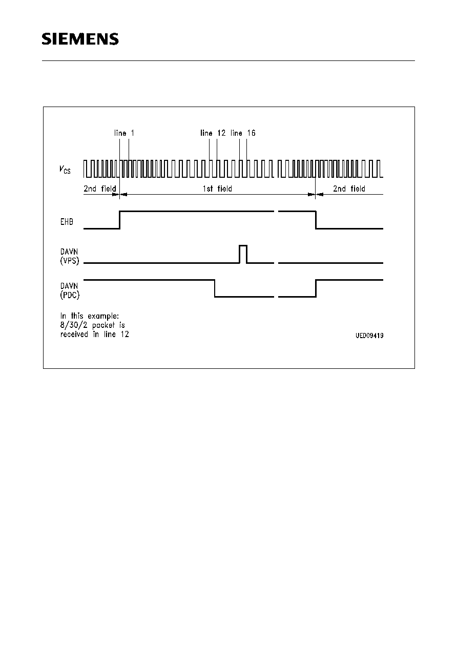
2.5
Description of DAVN and EHB Outputs
DAVN
(Data Valid active low)
EHB
(First Field active high)
In test mode (i.e. TI = high), both DAVN and EHB are controlled by the CS0 pin and
reproduce the state of the CS0 input.
Signal Output
VPS Mode
PDC Mode
8/30/2 Mode
8/30/1 Mode
Header Time
DAVN
H/L-transition
(set low)
in line 16 when
valid VPS data is
received
in the line
carrying
valid
8/30/2 data
in the line
carrying
valid
8/30/1 data
in the line
carrying
valid
header
row X/0 data
L/H-transition
(set high)
at the start of
line 16
at the beginning of the next field
i.e., at the start of the next data entry window
always set high
on power-up or during
I
2
C-Bus accesses when the bus master
doesn't acknowledge in order to generate the stop condition
EHB
L/H-transition
at the beginning of the first field
H/L-transition
at the beginning of the second field

SDA 5650/X
Semiconductor Group
26
02.97
3
Electrical Characteristics
Absolute Maximum Ratings
T
A
= 25
∞
C
Parameter
Symbol
Limit Values
Unit Test
Condition
min.
typ.
max.
Ambient temperature
T
A
0
70
∞
C
in operation
Storage temperature
T
stg
≠ 40
125
∞
C
by storage
Total power dissipation
P
tot
300
mW
Power dissipation per
output
P
DQ
10
mW
Input voltage
V
IM
≠ 0.3
6
V
Supply voltage
V
DD
≠ 0.3
6
V
Thermal resistance
R
th SU
80
K/W
Note: Maximum ratings are absolute ratings; exceeding any one of these values may
cause irreversible damage to the integrated circuit.
Operating Range
Supply voltage
V
DD
4.5
5
5.5
V
Supply current
I
DD
5
15
mA
Ambient temperature
range
T
A
0
70
∞
C
Note: In the operating range the functions given in the circuit description are fulfilled.
SDA 5650/X
Semiconductor Group
27
02.97
Electrical Characteristics
T
A
= 25
∞
C
Parameter
Symbol
Limit Values
Unit Test Condition
min.
typ.
max.
Input Signals SDA, SCL, CS0
H-input voltage
V
IH
0.7
◊
V
DD
V
DD
V
L-input voltage
V
IL
0
0.3
◊
V
DD
V
Input capacitance
C
I
10
pF
Input current
I
IM
10
µ
A
Input Signal TI
H-input voltage
V
IH
0.9
◊
V
DD
V
DD
V
L-input voltage
V
IL
0
0.1
◊
V
DD
V
Input capacitance
C
I
10
pF
Input current
I
IM
10
µ
A
Input Signals CVBS
(pos. Video, neg. Sync)
Video input signal
level
V
CVBS
0.7
1.0
2.0
V
2 Vpp with
0.8 V
V
SYNC
and
1.2 V
V
DAT
Synchron signal
amplitude
V
SYNC
0.15
0.3
0.8 (1.0)
V
1.0 V only
related to VCS
signal generation
Data amplitude
V
DAT
0.25
1.5
◊
V
SYNC
0.5
1.2
V
Coupling capacitor
C
C
33
nF
H-input current
I
IH
10
µ
A
V
I
= 5 V
L-input current
I
IL
≠ 1000
≠ 400 ≠ 100
µ
A
V
I
= 0 V
Source impedance
R
S
250
Leakage resistance
at coupling capacitor
R
C
0.91
1
1.2
M

SDA 5650/X
Semiconductor Group
28
02.97
Output Signals DAVN, EHB, VCS
H-output voltage
V
QH
V
DD
≠ 0.5
V
I
Q
= ≠ 100
µ
A
L-output voltage
V
QL
0.4
V
I
Q
= 1.6 mA
Output Signals SDA (Open-Drain-Stage)
L-output voltage
V
QL
0.4
V
I
Q
= 3.0 mA
Permissible output
voltage
5.5
V
PLL-Loop Filter Components (see application circuit)
Resistance at PD2/
VCO2
R
1
6.8
k
Resistance at VCO1
R
2
1200
k
Attenuation
resistance
R
3
6.8
k
Resistance at PD2/
VCO2
R
5
1200
k
Integration capacitor
C
1
2.2
nF
Integration capacitor
C
3
33
nF
VCO ≠ Frequence Range Adjustment
Resistance at IREF
(for bias current
adjustment)
R
4
100
k
Note: The listed characteristics are ensured over the operating range of the integrated
circuit. Typical characteristics specify mean values expected over the production
spread. If not otherwise specified, typical characteristics apply at
T
A
= 25
∞
C and
the given supply voltage.
Electrical Characteristics (cont'd)
T
A
= 25
∞
C
Parameter
Symbol
Limit Values
Unit Test Condition
min.
typ.
max.

SDA 5650/X
Semiconductor Group
29
02.97
Figure 3
I
2
C-Bus Timing
All values referred to
V
IH
and
V
IL
levels.
Parameter
Symbol
Limit Values
Unit
min.
max.
Clock frequency
f
SCL
0
100
kHz
Inactive time prior to new transmission start-up
t
BUF
4.7
µ
s
Hold time during start condition
t
HD; STA
4.0
µ
s
Low-period of clock
t
LOW
4.7
µ
s
High-period of clock
t
HIGH
4.0
µ
s
Set-up time for data
t
SU;DAT
250
ns
Rise time for SDA and SCL signal
t
TLH
1
µ
s
Fall time for SDA and SCL signal
t
THL
300
ns
Set-up time for SCL clock during stop condition
t
SU; STO
4.7
µ
s
SDA 5650/X
Semiconductor Group
30
02.97
4
PDC/VPS-Receiver
Figure 4
SDA 5650/X
Semiconductor Group
31
02.97
5
Appendix
5.1
Control Register Write (
I
2
C-Bus Write)
Figure 5
5.2
Data Register Read (
I
2
C-Bus Read)
Figure 6
SDA 5650/X
Semiconductor Group
32
02.97
5.3
DAVN and EHB Timing
Figure 7

SDA 5650/X
Semiconductor Group
33
02.97
5.4
Position of Teletext and VPS Data Lines within the Vertical Blanking
Interval
Figure 8
5.5
Definition of Voltage Levels for VPS Data Line
Figure 9
SDA 5650/X
Semiconductor Group
34
02.97
5.6
BDSP 8/30 Format 1 Bit Allocation
Note: This corresponds to the coding adopted in CCIR teletext system B BDSP 8/30
format 1.
NB: The received bytes are output on the
I
2
C Bus in a transparent way, i.e., on a
bit-first-in-first-out basis. No bit manipulation is performed on the chip in this
operating mode.
Concerning bytes no. 16 through 21: When evaluating the numbers, note that
each 4-bit-digit has been incremented by one prior to transmission, and the least
significant bits are transmitted first.
Byte No.
Bit No.
Contents
0
1
2
3
4
5
6
7
13
Network Identification 1. Byte
14
Network Identification 2. Byte
15
Weight
Weight
Sign
Time Offset Code
2
≠ 2
2
≠ 1
2
0
2
1
2
2
2
3
0
1
16
MJD Digit
Weight 10
4
1
1
1
1
Modified Julian Date (MJD)
1. Byte
17
MJD Digit
Weight 10
2
MJD Digit
Weight 10
3
Modified Julian Date
2. Byte
18
MJD Digit
Weight 10
0
MJD Digit
Weight 10
1
Modified Julian Date (MJD)
3. Byte
19
UTC Hours
Units
UTC Hours
Tens
Universal Time Coordinated
(UTC)
1. Byte
20
UTC Minutes
Units
UTC Minutes
Tens
Universal Time Coordinated
2. Byte
21
UTC Seconds
Units
UTC Seconds
Tens
Universal Time Coordinated
3. Byte
22
Short Programme Label 1. Byte
23
Short Programme Label 2. Byte
24
Short Programme Label 3. Byte
25
Short Programme Label 4. Byte
SDA 5650/X
Semiconductor Group
35
02.97
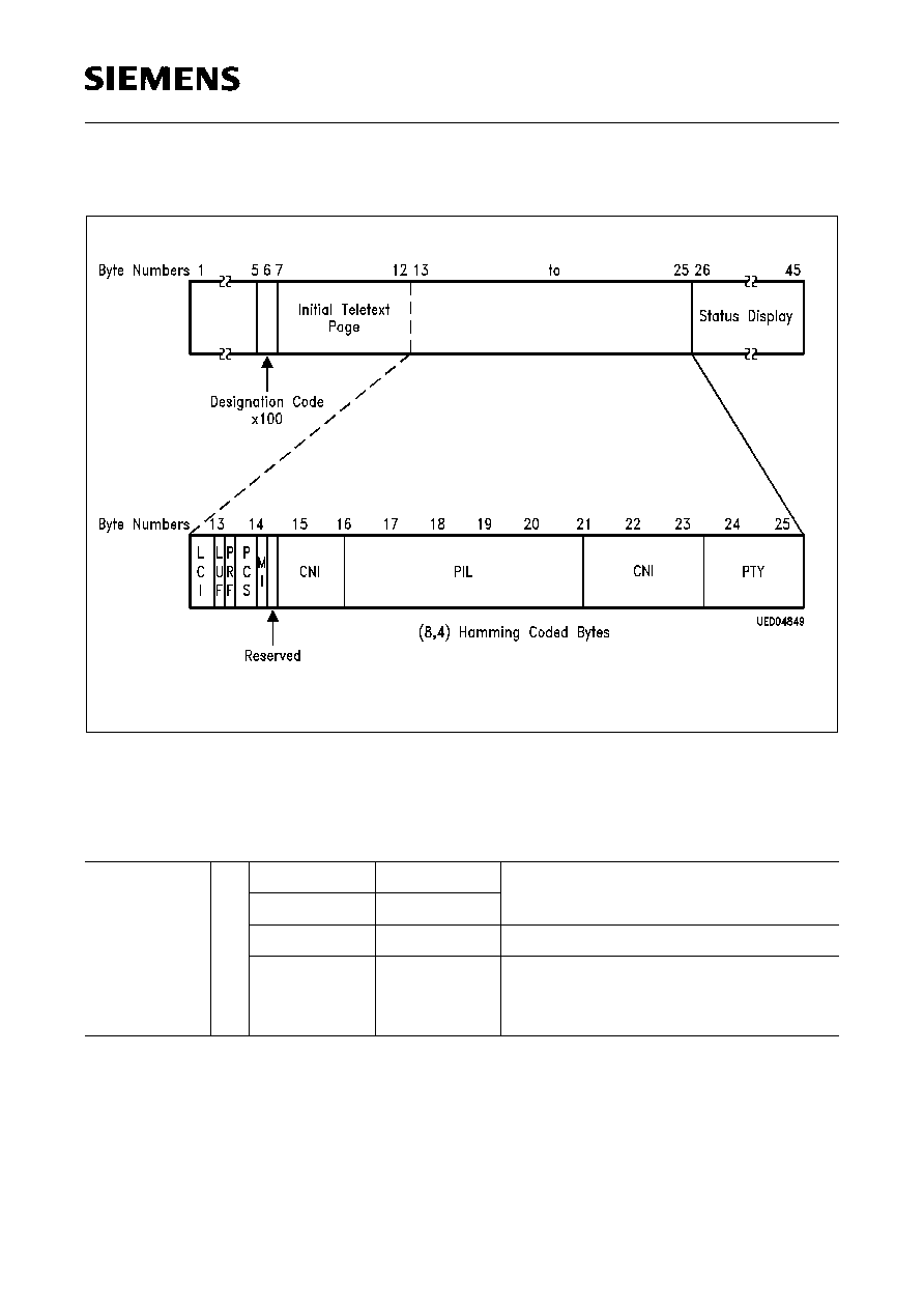
5.7
Structure of the Teletext Data Packet 8/30 Format 2
Figure 10
:
5.8
BDSP 8/30 Format 2 Bit Allocation
The four message bits of byte 13 are used as follows
byte 13
bit 0 ≠ LCI
b
1
label channel identifier
1 ≠ LCI
b
2
2 ≠ LUF
label update flag
3 ≠ reserved
but as yet
undefined

SDA 5650/X
Semiconductor Group
36
02.97
The message bits of bytes 14-25 are used in a way similar to the coding of the label in
the dedicated television line as follows:
byte 14
bit 0 PCS
b
1
status of analogue sound
1 PCS
b
2
2
reserved but yet
3
undefined
byte 15
bit 0 CNI
b
1
country
1 CNI
b
2
2 CNI
b
3
3 CNI
b
4
byte 16
bit 0 CNI
b
9
network (or programme provider)
1 CNI
b
10
2 PIL
b
1
day
3 PIL
b
2
byte 17
bit 0 PIL
b
3
1 PIL
b
4
2 PIL
b
5
3 PIL
b
6
month
byte 18
bit 0 PIL
b
7
1 PIL
b
8
2 PIL
b
9
3 PIL
b
10
hour
byte 19
bit 0 PIL
b
11
1 PIL
b
12
2 PIL
b
13
3 PIL
b
14
5.8
BDSP 8/30 Format 2 Bit Allocation (cont'd)
SDA 5650/X
Semiconductor Group
37
02.97
byte 20
bit 0 PIL
b
15
minute
1 PIL
b
16
2 PIL
b
17
3 PIL
b
18
byte 21
bit 0 PIL
b
19
1 PIL
b
20
2 CNI
b
5
country
3 CNI
b
6
byte 22
bit 0 CNI
b
7
1 CNI
b
8
2 CNI
b
11
network (or programme provider)
3 CNI
b
12
byte 23
bit 0 CNI
b
13
1 CNI
b
14
2 CNI
b
15
3 CNI
b
16
byte 24
bit 0 PTY
b
1
programme type
1 PTY
b
2
2 PTY
b
3
3 PTY
b
4
byte 25
bit 0 PTY
b
5
1 PTY
b
6
2 PTY
b
7
3 PTY
b
8
5.8
BDSP 8/30 Format 2 Bit Allocation (cont'd)

SDA 5650/X
Semiconductor Group
38
02.97
5.9
Data Format of Programme Delivery Data in the Dedicated TV Line (VPS)
Figure 11
SDA 5650/X
Semiconductor Group
39
02.97
Figure 12

SDA 5650/X
Semiconductor Group
40
02.97
6
Package Outlines
P-DIP-14-1
(Plastic Dual In-line Package)
GPD05005
Sorts of Packing
Package outlines for tubes, trays etc. are contained in our
Data Book "Package Information".
Dimensions in mm
SDA 5650/X
Semiconductor Group
41
02.97
P-DSO-20-1
(Plastic Dual Small Outline Package)
GPS05094
Sorts of Packing
Package outlines for tubes, trays etc. are contained in our
Data Book "Package Information".
Dimensions in mm
SMD = Surface Mounted Device