
Semiconductor Group
1
1998-10-01
∑ 1 048 576 words by 16-bit organization
∑ 0 to 70
∞
C operating temperature
∑ Fast Page Mode operation
∑ Performance:
∑ Power Dissipation, Refresh & Addressing:
∑ Read, write, read-modify-write, CAS-before-RAS refresh, RAS-only refresh and hidden refresh
∑ All inputs, outputs and clocks fully TTL (5 V versions) and LV-TTL (3.3 V version)-compatible
∑ Plastic Package:
P-SOJ-42-1
400 mil
-50
-60
t
RAC
RAS access time
50
60
ns
t
CAC
CAS access time
13
15
ns
t
AA
Access time from address
25
30
ns
t
RC
Read/Write cycle time
84
104
ns
t
PC
Fast page mode cycle time
35
40
ns
HYB5118160
HYB3118160
-50
-60
-50
-60
Power Supply
5 V
±
10 %
3.3 V
±
0.3 V
Addressing
10/10
10/10
Refresh
1024 cycles / 16 ms
Active
715
632
468
414
mW
TTL Standby
11
7.2
mW
CMOS Standby
5.5
3.6
mW
1M
◊
16-Bit Dynamic RAM
1k Refresh
(Fast Page Mode)
Advanced Information
HYB 5118160BSJ-50/-60
HYB 3118160BSJ-50/-60

HYB 5118160BSJ-50/-60
HYB 3118160BSJ-50/-60
1M
◊
16 DRAM
Semiconductor Group
2
1998-10-01
The HYB 5(3)118160 are 16 MBit dynamic RAMs based on die revisions "G" & "F" and organized
as 1 048 576 words by 16-bits. The HYB 5(3)118)160 utilizes a submicron CMOS silicon gate
process technology, as well as advanced circuit techniques to provide wide operating margins, both
internally and for the system user. Multiplexed address inputs permit the HYB 5(3)118160 to be
packaged in a standard SOJ-42 plastic package with 400 mil width. This package provide high
system bit densities and is compatible with commonly used automatic testing and insertion
equipment.
Ordering Information
Type
Ordering Code
Package
Descriptions
HYB 5118160BSJ-50
Q67100-Q1072
P-SOJ-42-1 400 mil
5 V
50 ns FPM-DRAM
HYB 5118160BSJ-60
Q67100-Q1073
P-SOJ-42-1 400 mil
5 V
60 ns FPM-DRAM
HYB 3118160BSJ-50
on request
P-SOJ-42-1 400 mil
3.3 V 50 ns FPM-DRAM
HYB 3118160BSJ-60
on request
P-SOJ-42-1 400 mil
3.3 V 60 ns FPM-DRAM
Pin Names
HYB 5(3)118160
Row Address Inputs
A0 - A9
Column Address Inputs
A0 - A9
Row Address Strobe
RAS
Upper Column Address Strobe
UCAS
Lower Column Address Strobe
LCAS
Output Enable
OE
Data Input/Output
I/O1 - I/O16
Read/Write Input
WE
Power Supply
V
CC
Ground (0 V)
V
SS
Not Connected
N.C.

HYB 5118160BSJ-50/-60
HYB 3118160BSJ-50/-60
1M
◊
16 DRAM
Semiconductor Group
3
1998-10-01
Pin Configuration
1
2
3
4
5
6
7
8
9
10
11
12
13
14
15
16
17
23
24
25
26
27
28
29
30
31
32
33
34
35
36
37
38
39
A5
A6
A7
OE
A8
UCAS
A9
I/O11
I/O13
I/O12
A0
A1
A2
I/O3
I/O4
I/O5
I/O6
I/O7
WE
RAS
N.C.
N.C.
SPP02812
V
SS
SS
V
CC
V
I/O8
I/O10
I/O16
I/O15
SS
V
I/O1
I/O2
V
CC
21
19
20
18
22
V
CC
N.C.
N.C.
A3
A4
LCAS
N.C.
42
41
40
I/O9
I/O14
P-SOJ-42 (400 mil)
HYB 5118160BSJ-50/-60
HYB 3118160BSJ-50/-60
1M
◊
16 DRAM
Semiconductor Group
4
1998-10-01
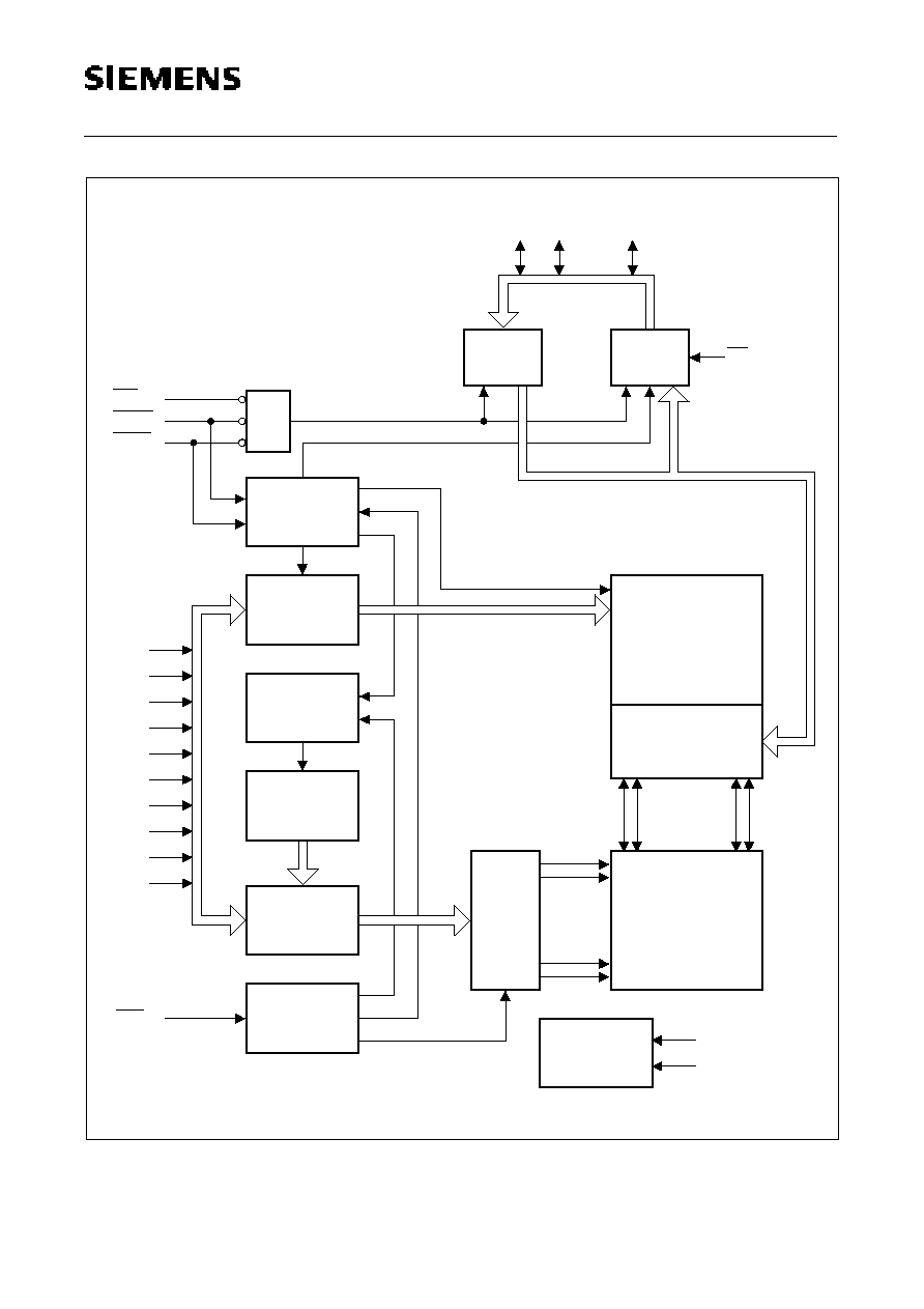
Block Diagram for HYB 5118160BSJ
Data In
Buffer
Data Out
Buffer
I/O1 I/O2
I/O16
OE
Column
Decoder
Sense Amplifier
I/O Gating
&
No.2 Clock
Generator
Column
Address
Buffers (10)
Refresh
Controller
Refresh
Counter (10)
Buffers (10)
Address
Row
No.1 Clock
Generator
10
10
Memory Array
Decoder
Row
.
.
.
.
.
.
. .
.
.. .
16
16
16
10
10
WE
LCAS
RAS
SPB02826
. . .
10
. . ..
UCAS
Generator
Voltage Down
V
CC
CC
V
(internal)
1024 x 1024 x 16
1024
1024
16
x
A9
A8
A7
A6
A5
A4
A3
A2
A1
A0
HYB 5118160BSJ-50/-60
HYB 3118160BSJ-50/-60
1M
◊
16 DRAM
Semiconductor Group
5
1998-10-01
Absolute Maximum Ratings
Operating temperature range ........................................................................................... 0 to 70
∞
C
Storage temperature range........................................................................................ ≠ 55 to 150
∞
C
Input/output voltage (5 V versions) .................................................... ≠ 0.5 to min (
V
CC
+ 0.5, 7.0) V
Input/output voltage (3.3 V versions) ................................................. ≠ 0.5 to min (
V
CC
+ 0.5, 4.6) V
Power supply voltage (5 V versions) ....................................................................... ≠ 1.0 V to 7.0 V
Power supply voltage (3.3 V versions) .................................................................... ≠ 1.0 V to 4.6 V
Power dissipation (5 V versions) ............................................................................................. 1.0 W
Power dissipation (3.3 V versions) .......................................................................................... 0.5 W
Data out current (short circuit) ................................................................................................ 50 mA
Note: Stresses above those listed under
"
Absolute Maximum Ratings
"
may cause permanent
damage of the device. Exposure to absolute maximum rating conditions for extended periods
may affect device reliability.
DC Characteristics
T
A
= 0 to 70
∞
C,
V
SS
= 0 V,
t
T
= 2 ns
Parameter
Symbol
Limit Values
Unit Test
Condition
min.
max.
5 V Versions
Power supply voltage
V
CC
4.5
5.5
V
Input high voltage
V
IH
2.4
V
CC
+ 0.5 V
1
Input low voltage
V
IL
≠ 0.5
0.8
V
1
Output high voltage (
I
OUT
= ≠ 5 mA)
V
OH
2.4
≠
V
1
Output low voltage (
I
OUT
= 4.2 mA)
V
OL
≠
0.4
V
1
3.3 V Versions
Power supply voltage
V
CC
3.0
3.6
V
Input high voltage
V
IH
2.0
V
CC
+ 0.5 V
1
Input low voltage
V
IL
≠ 0.5
0.8
V
1
TTL Output high voltage (
I
OUT
= ≠ 2 mA)
V
OH
2.4
≠
V
1
TTL Output low voltage (
I
OUT
= 2 mA)
V
OL
≠
0.4
V
1
CMOS Output high voltage (
I
OUT
= ≠ 100
µ
A)
V
OH
V
CC
≠ 0.2 ≠
V
CMOS Output low voltage (
I
OUT
= 100
µ
A)
V
OL
≠
0.2
V

HYB 5118160BSJ-50/-60
HYB 3118160BSJ-50/-60
1M
◊
16 DRAM
Semiconductor Group
6
1998-10-01
DC Characteristics (cont'd)
T
A
= 0 to 70
∞
C,
V
SS
= 0 V,
t
T
= 2 ns
Parameter
Symbol
Limit
Values
Unit
Notes
min.
max.
Common Parameters
Input leakage current
(0 V
V
IH
V
CC
+ 0.3 V, all other pins = 0 V)
I
I(L)
≠ 10
10
µ
A
1
Output leakage current
(DO is disabled, 0 V
V
OUT
V
CC
+ 0.3 V)
I
O(L)
≠ 10
10
µ
A
1
Average
V
CC
supply current
-50 ns version
-60 ns version
(RAS, CAS, address cycling:
t
RC
=
t
RC MIN.
)
I
CC1
≠
≠
130
115
mA
mA
2, 3, 4
2, 3, 4
Standby
V
CC
supply current (RAS = CAS =
V
IH
)
I
CC2
≠
2
mA
≠
Average
V
CC
supply current, during RAS-only refresh
cycles
-50 ns version
-60 ns version
(RAS cycling, CAS =
V
IH
,
t
RC
=
t
RC MIN.
)
I
CC3
≠
≠
130
115
mA
mA
2, 4
2, 4
Average
V
CC
supply current, during fast page mode
-50 ns version
-60 ns version
(RAS =
V
IL
, CAS, address cycling:
t
PC
=
t
PC MIN.
)
I
CC4
≠
≠
40
30
mA
mA
2, 3, 4
2, 3, 4
Standby
V
CC
supply current
(RAS = CAS =
V
CC
≠ 0.2 V)
I
CC5
≠
1
mA
1
Average
V
CC
supply current, during CAS-before-RAS
refresh mode
-50 ns version
-60 ns version
(RAS, CAS cycling:
t
RC
=
t
RC MIN.
)
I
CC6
≠
≠
130
115
mA
mA
2, 4
2, 4

HYB 5118160BSJ-50/-60
HYB 3118160BSJ-50/-60
1M
◊
16 DRAM
Semiconductor Group
7
1998-10-01
Capacitance
T
A
= 0 to 70
∞
C,
f
= 1 MHz
Parameter
Symbol
Limit Values
Unit
min.
max.
Input capacitance (A0 to A11)
C
I1
≠
5
pF
Input capacitance (RAS, UCAS, LCAS, WE, OE)
C
I2
≠
7
pF
I/O capacitance (I/O1 - I/O16)
C
IO
≠
7
pF
AC Characteristics
5, 6
T
A
= 0 to 70
∞
C,
V
CC
= 5 V
±
10 % /
V
CC
= 3.3 V
±
0.3 V,
t
T
= 5 ns
Parameter
Symbol
Limit Values
Unit Note
-50
-60
min.
max. min.
max.
Common Parameters
Random read or write cycle time
t
RC
90
≠
110
≠
ns
RAS precharge time
t
RP
30
≠
40
≠
ns
RAS pulse width
t
RAS
50
10k
60
10k
ns
CAS pulse width
t
CAS
13
10k
15
10k
ns
Row address setup time
t
ASR
0
≠
0
≠
ns
Row address hold time
t
RAH
8
≠
10
≠
ns
Column address setup time
t
ASC
0
≠
0
≠
ns
Column address hold time
t
CAH
10
≠
15
≠
ns
RAS to CAS delay time
t
RCD
18
37
20
45
RAS to column address delay time
t
RAD
13
25
15
30
ns
RAS hold time
t
RSH
13
≠
15
≠
ns
CAS hold time
t
CSH
50
≠
60
≠
ns
CAS to RAS precharge time
t
CRP
5
≠
5
≠
ns
Transition time (rise and fall)
t
T
3
50
3
50
ns
7
Refresh period for 1k-refresh version
t
REF
≠
16
≠
16
ms
Read Cycle
Access time from RAS
t
RAC
≠
50
≠
60
ns
8 ,9
Access time from CAS
t
CAC
≠
13
≠
15
ns
8, 9
Access time from column address
t
AA
≠
25
≠
30
ns
8, 10
OE access time
t
OEA
≠
13
≠
15
ns
HYB 5118160BSJ-50/-60
HYB 3118160BSJ-50/-60
1M
◊
16 DRAM
Semiconductor Group
8
1998-10-01
Column address to RAS lead time
t
RAL
25
≠
30
≠
ns
Read command setup time
t
RCS
0
≠
0
≠
ns
Read command hold time
t
RCH
0
≠
0
≠
ns
11
Read command hold time referenced to RAS
t
RRH
0
≠
0
≠
ns
11
CAS to output in low-Z
t
CLZ
0
≠
0
≠
ns
8
Output buffer turn-off delay
t
OFF
0
13
0
15
ns
12
Output buffer turn-off delay from OE
t
OEZ
0
13
0
15
ns
12
Data to OE low delay
t
DZO
0
≠
0
≠
ns
13
CAS high to data delay
t
CDD
13
≠
15
≠
ns
14
OE high to data delay
t
ODD
13
≠
15
≠
ns
14
Write Cycle
Write command hold time
t
WCH
8
≠
10
≠
ns
Write command pulse width
t
WP
8
≠
10
≠
ns
Write command setup time
t
WCS
0
≠
0
≠
ns
15
Write command to RAS lead time
t
RWL
13
≠
15
≠
ns
Write command to CAS lead time
t
CWL
13
≠
15
≠
ns
Data setup time
t
DS
0
≠
0
≠
ns
16
Data hold time
t
DH
10
≠
10
≠
ns
16
Data to CAS low delay
t
DZC
0
≠
0
≠
ns
13
Read-Modify-Write Cycle
Read-write cycle time
t
RWC
126
≠
150
≠
ns
RAS to WE delay time
t
RWD
68
≠
80
≠
ns
15
CAS to WE delay time
t
CWD
31
≠
35
≠
ns
15
Column address to WE delay time
t
AWD
43
≠
50
≠
ns
15
OE command hold time
t
OEH
13
≠
15
≠
ns
Fast Page Mode Cycle
Fast page mode cycle time
t
PC
35
≠
40
≠
ns
CAS precharge time
t
CP
10
≠
10
≠
ns
AC Characteristics (cont'd)
5, 6
T
A
= 0 to 70
∞
C,
V
CC
= 5 V
±
10 % /
V
CC
= 3.3 V
±
0.3 V,
t
T
= 5 ns
Parameter
Symbol
Limit Values
Unit Note
-50
-60
min.
max. min.
max.
HYB 5118160BSJ-50/-60
HYB 3118160BSJ-50/-60
1M
◊
16 DRAM
Semiconductor Group
9
1998-10-01
Access time from CAS precharge
t
CPA
≠
30
≠
35
ns
7
RAS pulse width
t
RAS
50
200k
60
200k
ns
CAS precharge to RAS Delay
t
RHPC
30
≠
35
≠
ns
Fast Page Mode Read-Modify-Write Cycle
Fast page mode read-write cycle time
t
PRWC
71
≠
80
≠
ns
CAS precharge to WE
t
CPWD
48
≠
55
≠
ns
CAS-before-RAS Refresh Cycle
CAS setup time
t
CSR
10
≠
10
≠
ns
CAS hold time
t
CHR
10
≠
10
≠
ns
RAS to CAS precharge time
t
RPC
5
≠
5
≠
ns
Write to RAS precharge time
t
WRP
10
≠
10
≠
ns
Write hold time referenced to RAS
t
WRH
10
≠
10
≠
ns
CAS-before-RAS Counter Test Cycle
CAS precharge time
t
CPT
35
≠
40
≠
ns
AC Characteristics (cont'd)
5, 6
T
A
= 0 to 70
∞
C,
V
CC
= 5 V
±
10 % /
V
CC
= 3.3 V
±
0.3 V,
t
T
= 5 ns
Parameter
Symbol
Limit Values
Unit Note
-50
-60
min.
max. min.
max.

HYB 5118160BSJ-50/-60
HYB 3118160BSJ-50/-60
1M
◊
16 DRAM
Semiconductor Group
10
1998-10-01
Notes
1. All voltages are referenced to
V
SS
.
2.
I
CC1
,
I
CC3
,
I
CC4
and
I
CC6
depend on cycle rate.
3.
I
CC1
and
I
CC4
depend on output loading. Specified values are measured with the output open.
4. Address can be changed once or less while RAS =
V
IL
. In the case of
I
CC4
it can be changed once
or less during a fast page mode cycle (
t
PC
).
5. An initial pause of 200
µ
s is required after power-up followed by 8 RAS cycles of which at least
one cycle has to be a refresh cycle, before proper device operation is achieved. In case of using
internal refresh counter, a minimum of 8 CAS-before-RAS initialization cycles instead of 8 RAS
cycles are required.
6. AC measurements assume
t
T
= 5 ns.
7.
V
IH (MIN.)
and
V
IL (MAX.)
are reference levels for measuring timing of input signals. Transition times
are also measured between
V
IH
and
V
IL
.
8. Measured with a load equivalent to 100 pF and at
V
OH
= 2.0 V (
I
OH
= ≠ 2 mA),
V
OL
= 0.8 V
(
I
OL
= 2 mA).
9. Operation within the
t
RCD (MAX.)
limit ensures that
t
RAC (MAX.)
can be met.
t
RCD (MAX.)
is specified as
a reference point only: If
t
RCD
is greater than the specified
t
RCD (MAX.)
limit, then access time is
controlled by
t
CAC
.
10.Operation within the
t
RAD (MAX.)
limit ensures that
t
RAC (MAX.)
can be met.
t
RAD (MAX.)
is specified as
a reference point only: If
t
RAD
is greater than the specified
t
RAD (MAX.)
limit, then access time is
controlled by
t
AA
.
11.Either
t
RCH
or
t
RRH
must be satisfied for a read cycle.
12.
t
OFF (MAX.)
and
t
OEZ (MAX.)
define the time at which the outputs achieve the open-circuit condition
and are not referenced to output voltage levels.
13.Either
t
DZC
or
t
DZO
must be satisfied.
14.Either
t
CDD
or
t
ODD
must be satisfied.
15.
t
WCS
,
t
RWD
,
t
CWD
,
t
AWD
and
t
CPWD
are not restrictive operating parameters. They are included in the
data sheet as electrical characteristics only. If
t
WCS
>
t
WCS (MIN.)
, the cycle is an early write cycle
and the I/O pin will remain open-circuit (high impedance) through the entire cycle; if
t
RWD
>
t
RWD (MIN.)
,
t
CWD
>
t
CWD (MIN.)
,
t
AWD
>
t
AWD (MIN.)
and
t
CPWD
>
t
CPWD (MIN.)
, the cycle is a read-
write cycle and I/O pins will contain data read from the selected cells. If neither of the above sets
of conditions is satisfied, the condition of the I/O pins (at access time) is indeterminate.
16.These parameters are referenced to the CAS leading edge in early write cycles and to the WE
leading edge in read-write cycles.

HYB 5118160BSJ-50/-60
HYB 3118160BSJ-50/-60
1M
◊
16 DRAM
Semiconductor Group
11
1998-10-01
Read Cycle
SPT03043
"H" or "L"
OEA
CAC
RAL
t
OH
OL
V
(Inputs)
(Outputs)
I/O
I/O
V
IH
V
IL
V
OE
WE
V
IL
V
IH
V
IL
V
IH
RAC
t
Hi
DZO
Z
t
CLZ
t
t
DZC
t
RCS
AA
t
t
LCAS
V
Address
V
IL
V
IH
IL
UCAS
RAS
IL
V
IH
V
V
IH
t
RAD
ASR
t
Row
t
Column
RAH
ASC
t
CAH
t
t
RCD
t
CSH
t
t
RAS
t
t
ODD
RRH
Valid Data OUT
OEZ
t
t
CDD
OFF
t
Hi Z
t
t
RSH
CAS
t
RC
t
RCH
ASR
t
Row
CRP
t
t
RP

HYB 5118160BSJ-50/-60
HYB 3118160BSJ-50/-60
1M
◊
16 DRAM
Semiconductor Group
12
1998-10-01
Write Cycle (Early Write)
SPT03044
"H" or "L"
RWL
RAL
WCS
OH
(Inputs)
(Outputs)
I/O
I/O
IL
V
OL
V
V
V
IH
OE
WE
IH
V
IL
V
V
IL
V
IH
t
DS
t
Valid
DH
Data IN
WCH
t
t
WP
t
LCAS
V
Address
IH
V
V
IL
IL
UCAS
RAS
V
IH
IH
V
V
IL
t
RAD
ASR
t
t
RAH
Row
t
Column
ASC
t
CWL
t
CAH
t
t
RCD
t
CSH
t
t
RAS
t
Z
Hi
t
RC
CAS
RSH
t
ASR
t
Row
CRP
t
t
RP

HYB 5118160BSJ-50/-60
HYB 3118160BSJ-50/-60
1M
◊
16 DRAM
Semiconductor Group
13
1998-10-01
Write Cycle (OE Controlled Write)
SPT03045
"H" or "L"
DS
RAL
CAS
V
OH
V
(Inputs)
(Outputs)
I/O
I/O
V
V
OL
IL
V
IH
OE
WE
V
IL
IL
V
IH
V
IH
t
DZO
Hi Z
t
CLZ
t
OEA
t
OEZ
t
DZC
ODD
t
t
V
Address
IL
V
V
IH
LCAS
UCAS
RAS
V
IL
V
IH
IL
V
IH
RAD
ASR
t
RAH
t
Row
t
t
Column
ASC
t
CAH
RCD
t
t
t
CSH
t
RAS
t
Hi
Valid Data
t
DH
OEH
t
Z
RWL
CWL
t
t
WP
t
RSH
t
ASR
t
Row
CRP
t
t
RC
t
RP

HYB 5118160BSJ-50/-60
HYB 3118160BSJ-50/-60
1M
◊
16 DRAM
Semiconductor Group
14
1998-10-01
Read-Write (Read-Modify-Write) Cycle
SPT03046
"H" or "L"
AWD
OEA
CSH
RWD
OH
I/O
(Outputs) V
OL
(Inputs)
I/O
IL
V
V
V
IH
OE
WE
V
IL
V
IH
V
IL
V
IH
RAC
t
t
DZC
t
DZO
t
CLZ
t
CAC
t
RCS
t
AA
t
V
Address
V
IL
V
IH
LCAS
UCAS
RAS
IH
V
IL
V
V
IL
IH
RAH
Row
ASR
t
t
RAD
t
Column
ASC
t
t
t
CAH
t
RCD
t
t
t
WP
Data
OUT
DS
ODD
OEZ
t
t
t
t
Data IN
Valid
t
DH
OEH
Row
t
CWD
t
CAS
t
t
RSH
RWL
t
t
CWL
ASR
t
CRP
t
RP
t
RWC
t
RAS
HYB 5118160BSJ-50/-60
HYB 3118160BSJ-50/-60
1M
◊
16 DRAM
Semiconductor Group
15
1998-10-01
Fast Page Mode Read Cycle
SPT03047
"H" or "L"
RASP
Column
WE
OH
OL
IH
IH
(Outputs)
I/O
V
V
(Inputs)
I/O
IL
V
V
OE
V
IL
V
V
IL
CLZ
Data OUT
Valid
RAC
t
DZC
t
t
t
t
CAC
DZO
t
OEZ
OFF
t
ODD
t
OEA
AA
t
t
DZC
t
IH
IH
IH
IH
Address
IL
V
V
V
LCAS
UCAS
V
IL
V
RAS
IL
V
V
t
Column
Row
ASR
t
RAD
RCS
t
t
ASC
t
t
RAH
RCD
t
t
CAH
t
RCH
ASC
t
PC
CSH
CAS
t
t
CP
t
t
OFF
CLZ
CLZ
Data OUT
Valid
Data OUT
Valid
t
t
t
t
CAC
DZO
OEZ
t
OFF
t
ODD
t
AA
t
CPA
t
OEA
t
DZC
t
t
CAC
t
DZO
OEZ
t
t
t
ODD
AA
t
CPA
t
OEA
t
CDD
t
RP
t
RCS
ASC
Column
CAH
t
RCS
t
t
t
CAS
t
t
CAH
t
RRH
RHCP
t
t
RSH
CAS
t
t
CRP
RCH
t
Row
ASR
t

HYB 5118160BSJ-50/-60
HYB 3118160BSJ-50/-60
1M
◊
16 DRAM
Semiconductor Group
16
1998-10-01
Fast Page Mode Early Write Cycle
SPT03048
"H" or "L"
Data IN
ASC
Column
WCS
t
t
WCS
IL
IH
IL
IH
OH
OL
IH
IL
(Outputs) V
OE
I/O
(Inputs)
I/O
V
V
V
V
WE
V
V
V
Data IN
DS
t
Valid
DH
t
DS
t
WCH
WP
t
t
IH
IL
IL
IH
IH
IL
Address
V
V
LCAS
RAS
UCAS
V
V
V
V
Column
Row
ASR
t
RAD
t
ASC
RAH
t
t
t
RCD
CWL
t
CAH
t
t
PC
t
CAS
t
CP
t
t
t
WCS
Valid
Hi Z
DH
t
t
DS
WCH
WP
t
t
Valid
Data IN
DH
t
WCH
WP
t
t
ASR
CRP
RASP
ASC
Column
t
CWL
CAH
t
t
t
CAS
t
RWL
CWL
t
RAL
CAH
t
t
t
t
RSH
CAS
t
t
t
RP
Row

HYB 5118160BSJ-50/-60
HYB 3118160BSJ-50/-60
1M
◊
16 DRAM
Semiconductor Group
17
1998-10-01
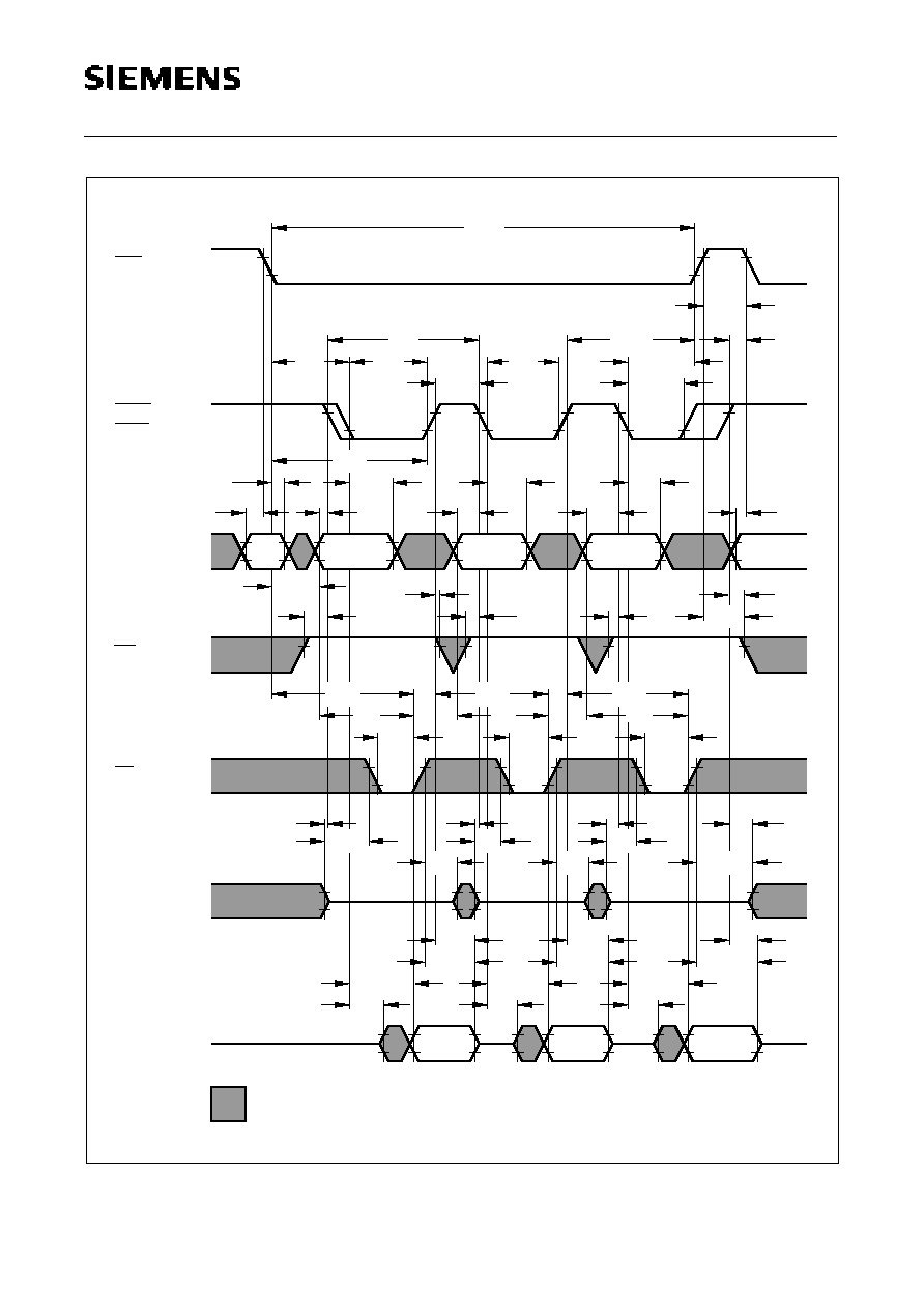
Fast Page Mode Late Write and Read-Modify-Write Cycle
SPT03049
"H" or "L"
IL
Data
RAC
(Outputs)
I/O
V
OH
OL
V
OUT
Data
OEZ
t
I/O
(Inputs)
OE
CLZ
t
V
IL
V
IH
DZC
t
t
CAC
t
DS
DZO
t
ODD
t
V
IL
IH
V
t
AWD
t
AA
t
OEA
t
t
OEH
AA
DS
AA
OUT
Data
t
OUT
Data
OEZ
OEZ
t
ODD
IN
DH
t
t
t
DZC
CPA
t
t
IN
Data
DH
t
t
t
CAC
t
DZC
t
t
CPA
OEH
CLZ
t
WP
t
t
OEA
t
AWD
t
CLZ
t
t
WP
OEA
t
AWD
t
IN
Data
DS
t
DH
t
ODD
t
WP
t
OEH
t
Address
WE
LCAS
UCAS
V
RCS
V
V
IH
t
Row
V
IL
IH
t
CWD
t
CWL
RWD
t
Column
IL
V
ASR
t
t
RAH
ASC
t
RAD
t
IH
V
RCD
t
t
CAH
CAS
t
RAS
IL
V
V
IH
t
CSH
CWD
CWL
t
CWD
t
Column
CPWD
t
t
t
CPWD
Column
PRWC
ASC
t
CAH
t
t
CP
CAS
t
t
ASC
t
t
CAH
CWL
t
RWL
t
Row
CRP
t
RAL
RSH
CAS
t
t
t
ASR
t
RAS
t
t
RP

HYB 5118160BSJ-50/-60
HYB 3118160BSJ-50/-60
1M
◊
16 DRAM
Semiconductor Group
18
1998-10-01
RAS-only Refresh Cycle
SPT03050
"H" or "L"
OH
OL
(Outputs)
Address
I/O
V
V
V
IL
IH
V
Row
LCAS
UCAS
RAS
IL
V
V
IH
V
IL
IH
V
RAH
ASR
t
t
RAS
t
Row
Z
Hi
t
RC
t
RPC
ASR
t
CRP
t
RP
t

HYB 5118160BSJ-50/-60
HYB 3118160BSJ-50/-60
1M
◊
16 DRAM
Semiconductor Group
19
1998-10-01
CAS-before-RAS Refresh Cycle
SPT03051
"H" or "L"
V
IL
IH
IH
IL
OL
OH
IL
(Outputs)
I/O
V
V
(Inputs)
OE
I/O
V
V
V
V
t
OFF
OEZ
t
t
CDD
ODD
t
IH
IL
IH
IH
IL
LCAS
WE
UCAS
V
V
V
RAS
V
V
WRP
CSR
t
t
CP
t
RPC
t
RP
t
t
WRH
t
CHR
Hi Z
RAS
t
RC
t
t
RPC
t
RP
CRP
t

HYB 5118160BSJ-50/-60
HYB 3118160BSJ-50/-60
1M
◊
16 DRAM
Semiconductor Group
20
1998-10-01
Hidden Refresh Cycle (Read)
SPT03053
"H" or "L"
V
I/O
(Outputs)
OL
V
(Inputs)
I/O
OH
V
V
IL
IH
V
OE
WE
V
IL
IH
V
IL
IH
V
CLZ
RAC
t
t
DZO
t
t
DZC
t
CAC
OEA
AA
t
t
Address
V
IL
IH
V
LCAS
UCAS
RAS
V
IL
IH
V
IL
V
IH
V
Column
RAS
t
t
RAH
Row
ASR
t
t
RCS
ASC
t
t
RCD
RAD
t
CAH
t
RRH
t
WRP
t
t
RSH
t
RC
RP
t
Valid Data OUT
OEZ
t
OFF
t
ODD
t
Hi Z
t
CDD
Row
WRH
t
t
CHR
RAS
t
ASR
t
CRP
t
RC
t
t
RP

HYB 5118160BSJ-50/-60
HYB 3118160BSJ-50/-60
1M
◊
16 DRAM
Semiconductor Group
21
1998-10-01
Hidden Refresh Cycle (Early Write)
SPT03054
"H" or "L"
WRP
Column
Row
Address
(Output)
(Input)
I/O
I/O
OL
V
OH
V
IN
V
V
IL
WE
IL
V
IH
V
V
IL
Valid Data
t
DS
t
WCS
t
DH
WP
t
WCH
t
t
ASR
V
LCAS
UCAS
IH
V
t
IL
IH
V
RAS
V
IL
IH
V
RAS
RAD
ASC
RAH
t
t
t
RCD
t
t
CAH
t
RSH
t
t
RC
RP
t
Row
Hi Z
t
WRH
RC
t
RAS
CHR
t
t
ASR
t
CRP
t
RP
t

HYB 5118160BSJ-50/-60
HYB 3118160BSJ-50/-60
1M
◊
16 DRAM
Semiconductor Group
22
1998-10-01
CAS-before-RAS Refresh Counter Test Cycle
SPT03055
"H" or "L"
t
WCH
t
t
DZC
t
(Inputs)
(Outputs)
I/O
I/O
OH
OL
V
IL
V
V
IH
V
Write Cycle
OE
WE
IL
IL
V
IH
V
V
IH
V
(Inputs)
(Outputs)
I/O
I/O
OL
V
OH
V
IL
V
IH
V
t
DS
Z
Hi
Data IN
t
WRP
WRH
t
DH
t
t
DZO
WCS
t
t
t
CLZ
OE
WE
IL
V
IH
V
IL
V
IH
V
LCAS
Address
UCAS
IH
IL
V
V
V
IL
IH
V
Read Cycle
RAS
V
IH
IL
V
WRP
t
WRH
t
t
RCS
AA
t
CAC
t
ASC
t
t
CAH
Column
CSR
t
CHR
t
CP
t
RAS
t
RWL
CWL
t
Data OUT
t
OEZ
t
OFF
t
ODD
OEA
t
RRH
RAL
CAS
t
CDD
t
RCH
t
t
ASR
Row
RSH
t
t
RP
HYB 5118160BSJ-50/-60
HYB 3118160BSJ-50/-60
1M
◊
16 DRAM
Semiconductor Group
23
1998-10-01
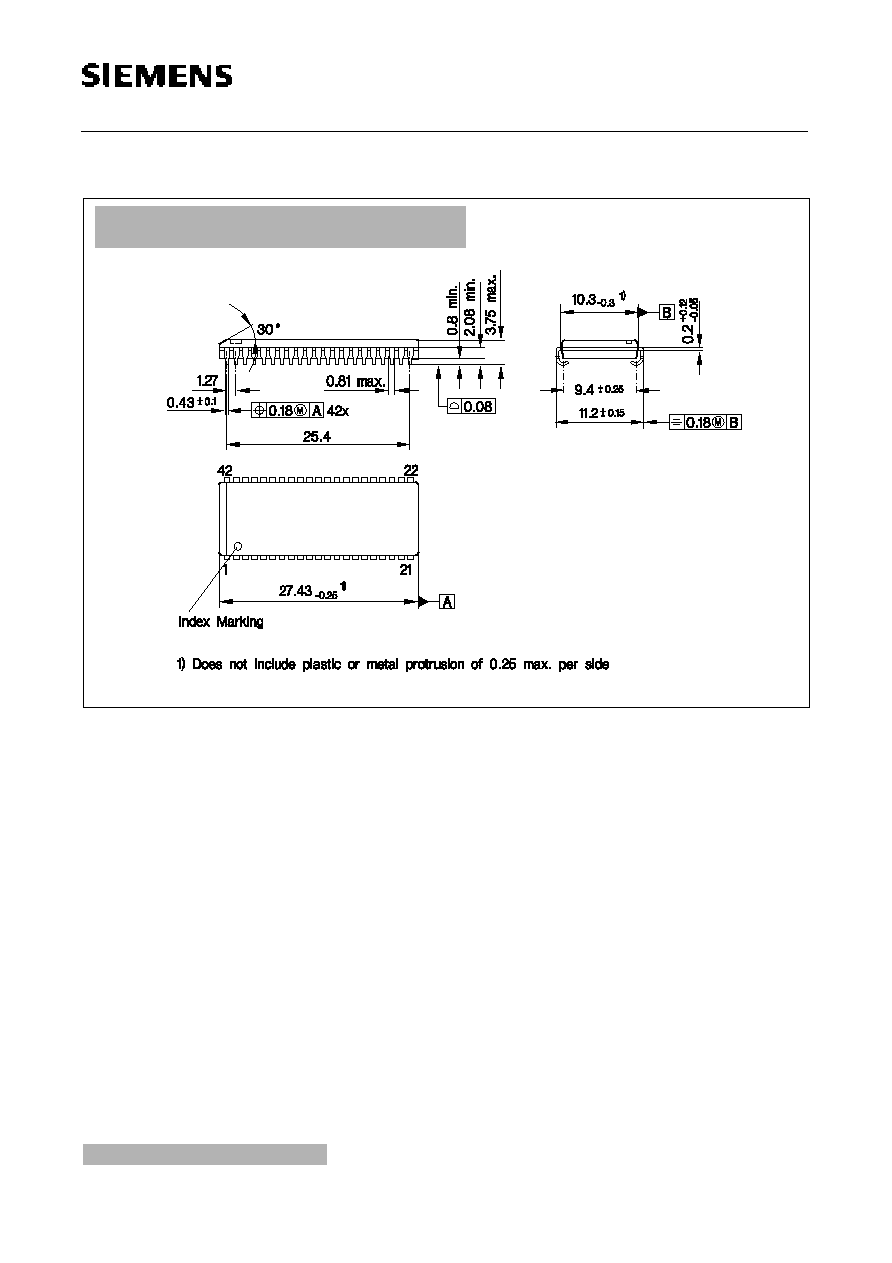
Package Outlines
Plastic Package P-SOJ-42-1 (SMD) (400mil)
(Plastic small outline J-leaded)
GPJ05853
Sorts of Packing
Package outlines for tubes, trays etc. are contained in our
Data Book "Package Information".
Dimensions in mm
SMD = Surface Mounted Device

HYB 5118160BSJ-50/-60
HYB 3118160BSJ-50/-60
1M
◊
16 DRAM
Semiconductor Group
24
1998-10-01
GPX05958
20.95
±0.13
1)
1
25
50
26
0.4
+0.05
-0.1
0.1
1
0.1
±0.2
11.76
±0.1
0.5
50x
±0.05
±0.05
0.15
-0.03
+0.06
15∞
±5∞
15∞
±5∞
6 max
2.5 max
11 15
10.16
±0.13
2)
3)
Index Marking
Does not include dambar protrusion of 0.13 max per side
Does not include plastic protrusion of 0.25 max per side
Does not include plastic or metal protrusion of 0.15 max per side
3)
2)
1)
0.8
19.2
24x 0.8 =
0.2
M
50x
36
40
Plastic Package P-TSOPII-50/44-1 (400 mil) (SMD)
(Plastic Thin Small Outline Package (Type II))
Sorts of Packing
Package outlines for tubes, trays etc. are contained in our
Data Book "Package Information".
Dimensions in mm
SMD = Surface Mounted Device