
Semiconductor Group 1 3.96
∑
4 194 304 words by 4-bit organization
∑
0 to 70 ∞C operating temperature
∑
Performance
∑
Single + 3.3 V (± 0.3V ) supply
∑
Low power dissipation
max. 396 active mW (HYB3117405BJ/BT-50)
max. 363 active mW (HYB3117405BJ/BT-60)
max. 330 active mW (HYB3117405BJ/BT-70)
max. 360 active mW (HYB3116405BJ/BT-50)
max. 324 active mW (HYB3116405BJ/BT-60)
max. 288 active mW (HYB3116405BJ/BT-70)
7.2 mW standby (LV-TTL)
3.6 mW standby (LV-CMOS)
720
µ
W standby for L-version
∑
Output unlatched at cycle end allows two-dimensional chip selection
∑
Read, write, read-modify-write, CAS-before-RAS refresh, RAS-only refresh, hidden refresh,
Self Refresh and test mode
∑
Hyper page mode (EDO) capability
∑
All inputs, outputs and clocks fully TTL-compatible
∑
2048 refresh cycles / 32 ms for HYB3117405
4096 refresh cycles / 64 ms for HYB3116405
∑
Plastic Package:
P-SOJ-26/24-1 (300 mil)
P-TSOPII-26/24-1 (300mil)
-50
-60
-70
tRAC
RAS access time
50
60
70
ns
tCAC
CAS access time
13
15
20
ns
tAA
Access time from address
25
30
35
ns
tRC
Read/Write cycle time
84
104
124
ns
tHPC
Hyper page mode (EDO)
cycle time
20
25
30
ns
3.3V 4M x 4-Bit EDO-Dynamic RAM
Advanced Information
HYB3116405BJ/BT(L) -50/-60/-70
HYB3117405BJ/BT(L) -50/-60/-70

Semiconductor Group
2
HYB 3116(7)405BJ/BT(L) -50/-60/-70
3.3V 4Mx4-DRAM
The HYB 3116(7)405BJ/BT(L) is a 16MBit dynamic RAM organized as 4194304 words by 4-bits.
The HYB 3116(7)405BJ/BT(L) utilizes a submicron CMOS silicon gate process technology, as well
as advanced circuit techniques to provide wide operating margins, both internally and for the system
user. Multiplexed address inputs permit the HYB 3116(7)405BJ/BT(L) to be packaged in a standard
SOJ 26/24 300 mil or TSOPII-26/24 300 mil wide plastic package. These packages provide high
system bit densities and are compatible with commonly used automatic testing and insertion
equipment. System-oriented features include single + 3.3 V (± 0.3 V) power supply, direct
interfacing with high-performance logic device families.The HYB3116405BTL parts have a very low
power ,,sleep mode" supported by Self Refresh.
Ordering Information
Type
Ordering Code
Package
Descriptions
HYB 3117405BJ-50
Q67100-Q1119
P-SOJ-26/24-1 300 mil
DRAM (access time 50 ns)
HYB 3117405BJ-60
Q67100-Q1120
P-SOJ-26/24-1 300 mil
DRAM (access time 60 ns)
HYB 3117405BJ-70
P-SOJ-26/24-1 300 mil
DRAM (access time 70 ns)
HYB 3117405BT-50
Q67100-Q1135
P-TSOPII-26/24-1 300 mil
DRAM (access time 50 ns)
HYB 3117405BT-60
Q67100-Q1136
P-TSOPII-26/24-1 300 mil
DRAM (access time 60 ns)
HYB 3117405BT-70
Q67100-Q1184
P-TSOPII-26/24-1 300 mil
DRAM (access time 70 ns)
HYB 3116405BJ-50
Q67100-Q1127
P-SOJ-26/24-1 300 mil
DRAM (access time 50 ns)
HYB 3116405BJ-60
Q67100-Q1128
P-SOJ-26/24-1 300 mil
DRAM (access time 60 ns)
HYB 3116405BJ-70
P-SOJ-26/24-1 300 mil
DRAM (access time 70 ns)
HYB 3116405BT-50
Q67100-Q1143
P-TSOPII-26/24-1 300 mil
DRAM (access time 50 ns)
HYB 3116405BT-60
Q67100-Q1144
P-TSOPII-26/24-1 300 mil
DRAM (access time 60 ns)
HYB 3116405BT-70
Q67100-Q1186
P-TSOPII-26/24-1 300 mil
DRAM (access time 70 ns)
HYB 3116405BTL-50
on request
P-TSOPII-26/24-1 300 mil
LP-DRAM (access time 50 ns)
HYB 3116405BTL-60
on request
P-TSOPII-26/24-1 300 mil
LP-DRAM (access time 60 ns)
HYB 3116405BTL-70
on request
P-TSOPII-26/24-1 300 mil
LP-DRAM (access time 70 ns)

Semiconductor Group
3
HYB 3116(7)405BJ/BT(L) -50/-60/-70
3.3V 4Mx4-DRAM
Pin Configuration
Pin Names
A0 to A10
Row & Column Address Inputs for HYB3117405
A0 to A11
Row Address Inputs for HYB3116405
A0 to A9
Column Address Inputs for HYB3116405
RAS
Row Address Strobe
OE
Output Enable
I/O1 -I/O4
Data Input/Output
CAS
Column Address Strobe
WE
Read/Write Input
V
CC
Power Supply (+ 3.3 V)
V
SS
Ground (0 V)
N.C.
not connected
P-SOJ-26/24-1 (300mil)
P-TSOPII-26/24-1 (300mil)
Vcc
I/O1
I/O2
WE
RAS
N.C.
A10
A0
A1
A2
A3
VCC
1
2
3
4
5
6
8
9
10
11
12
13
26
25
24
23
22
21
19
18
17
16
15
14
Vss
I/O4
I/O3
CAS
OE
A9
A8
A7
A6
A5
A4
Vss
HYB3117405BJ/BT
Vcc
I/O1
I/O2
WE
RAS
A11
A10
A0
A1
A2
A3
VCC
1
2
3
4
5
6
8
9
10
11
12
13
26
25
24
23
22
21
19
18
17
16
15
14
Vss
I/O4
I/O3
CAS
OE
A9
A8
A7
A6
A5
A4
Vss
HYB3116405BJ/BT

Semiconductor Group
4
HYB 3116(7)405BJ/BT(L) -50/-60/-70
3.3V 4Mx4-DRAM
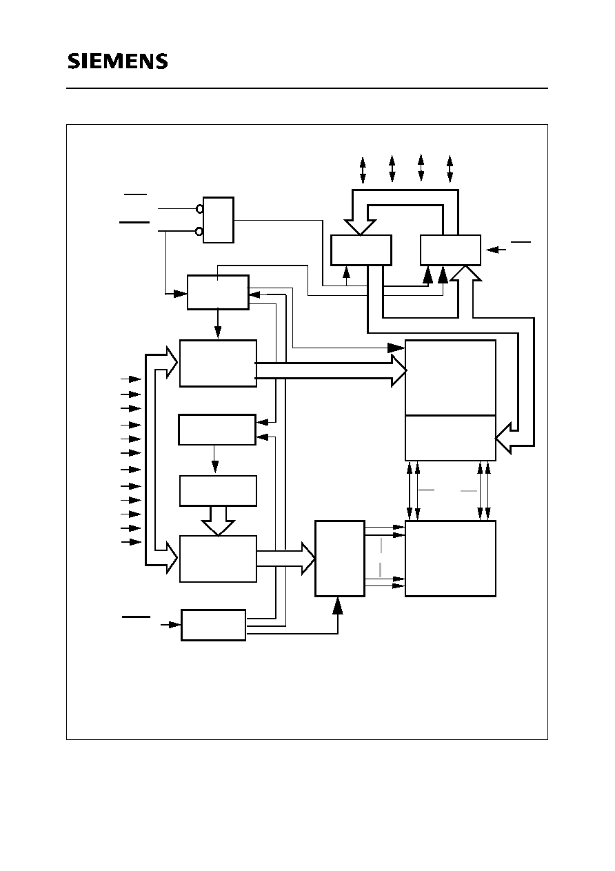
Block Diagram for HYB3117405
No. 2 Clock
Generator
Column
Address
Buffer(11)
Refresh
Controller
Refresh
Counter (11)
Address
Buffers(11)
Row
No. 1 Clock
Generator
&
Data in
Buffer
Data out
Buffer
Column
Decoder
Sense Amplifier
I/O Gating
Memory Array
2048x2048x4
Row
Decoder
A0
A1
A2
A3
A4
A5
A6
A7
A8
A9
WE
CAS
2048
2048
x4
.
RAS
11
11
11
4
4
4
I/O1 I/O2 I/O3 I/O4
OE
11
11
A10
Semiconductor Group
5
HYB 3116(7)405BJ/BT(L) -50/-60/-70
3.3V 4Mx4-DRAM
Block Diagram for HYB3116405
No. 2 Clock
Generator
Column
Address
Buffer(10)
Refresh
Controller
Refresh
Counter (12)
Address
Buffers(12)
Row
No. 1 Clock
Generator
&
Data in
Buffer
Data out
Buffer
Column
Decoder
Sense Amplifier
I/O Gating
Memory Array
4096x1024x4
Row
Decoder
A0
A1
A2
A3
A4
A5
A6
A7
A8
A9
WE
CAS
4096
1024
x4
.
RAS
10
12
10
4
4
4
I/O1 I/O2 I/O3 I/O4
OE
12
12
A10
A11

Semiconductor Group
6
HYB 3116(7)405BJ/BT(L) -50/-60/-70
3.3V 4Mx4-DRAM
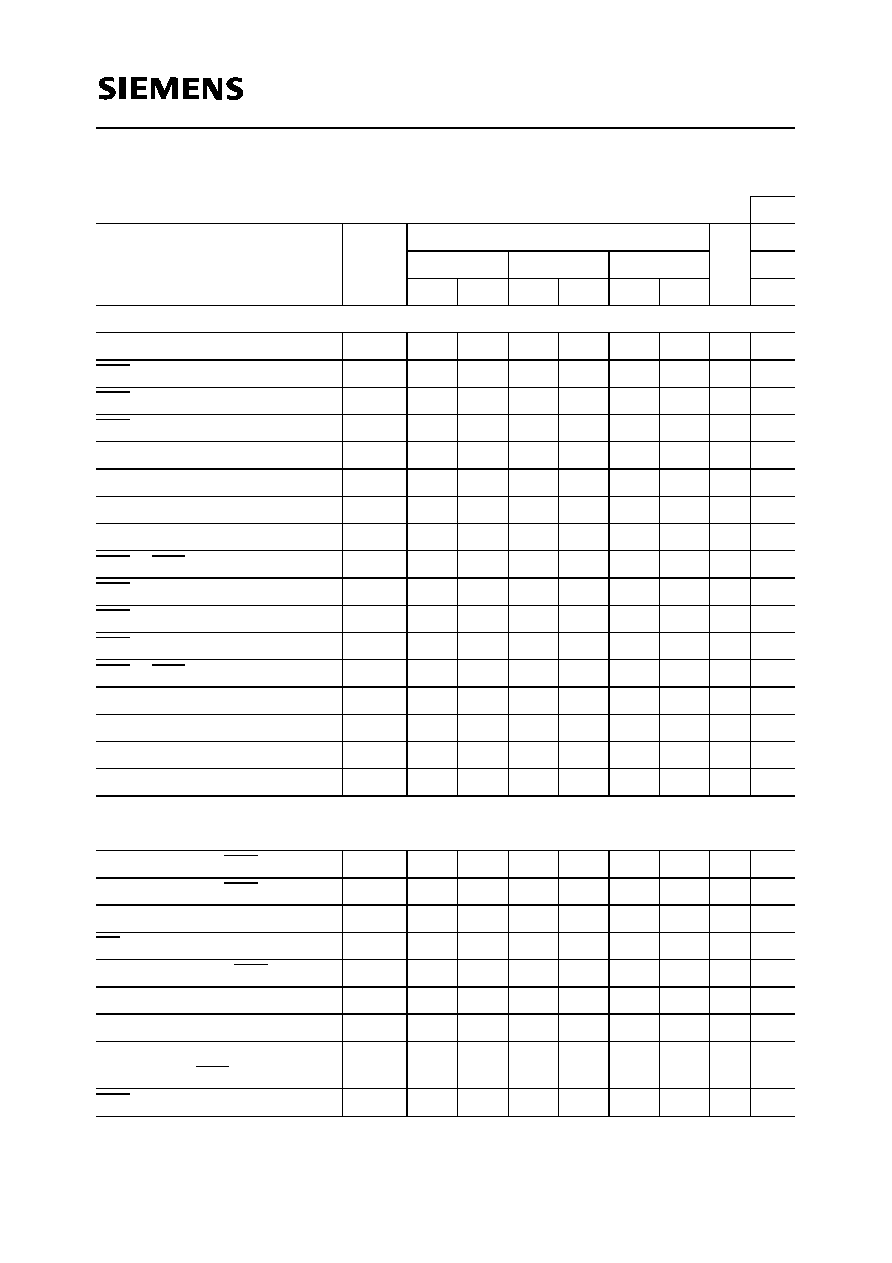
Absolute Maximum Ratings
Operating temperature range ............................................................................................0 to 70 ∞C
Storage temperature range.........................................................................................≠ 55 to 150 ∞C
Input/output voltage ................................................................................-0.5 to min(Vcc+0.5, 4.6) V
Power supply voltage.................................................................................................- 0.5 V to 4.6 V
Power dissipation.................................................................................................................... 0.5 W
Data out current (short circuit) ................................................................................................ 50 mA
Note:
Stresses above those listed under "Absolute Maximum Ratings" may cause permanent damage of
the device. Exposure to absolute maximum rating conditions for extended periods may affect device
reliability.
DC Characteristics (values in brackets for HYB3117405)
T
A
= 0 to 70 ∞C,
V
SS
= 0 V,
V
CC
= 3.3 V
±
0.3 V,
t
T
= 2 ns
Parameter
Symbol
Limit Values
Unit Test
Condition
min.
max.
Input high voltage
V
IH
2.0
Vcc+0.5
V
1)
Input low voltage
V
IL
≠ 0.5
0.8
V
1)
TTL Output high voltage (
I
OUT
= ≠ 2 mA)
V
OH
2.4
≠
V
1)
TTL Output low voltage (
I
OUT
= 2 mA)
V
OL
≠
0.4
V
1)
CMOS Output high voltage (
I
OUT
= ≠100 uA)
V
OH
VCC-0.2
≠
V
CMOS Output low voltage (
I
OUT
= 100 uA)
V
OL
≠
0.2
V
Input leakage current
(0 V
V
IH
Vcc + 0.3V, all other pins = 0 V)
I
I(L)
≠ 10
10
µ
A
1)
Output leakage current
(DO is disabled, 0 V
V
OUT
Vcc + 0.3V)
I
O(L)
≠ 10
10
µ
A
1)
Average
V
CC
supply current:
-50 ns version
-60 ns version
-70 ns version
(RAS, CAS, address cycling,
t
RC
=
t
RC
min.)
I
CC1
≠
≠
≠
100(120)
90 (110)
80 (100)
mA
mA
mA
2) 3) 4)
2) 3) 4)
2) 3) 4)
Standby
V
CC
supply current (RAS = CAS =
V
IH
)
I
CC2
≠
2
mA
≠

Semiconductor Group
7
HYB 3116(7)405BJ/BT(L) -50/-60/-70
3.3V 4Mx4-DRAM
Average
V
CC
supply current, during RAS-only
refresh cycles:
-50 ns version
-60 ns version
-70 ns version
(RAS cycling: CAS =
V
IH
,
t
RC
=
t
RC
min.)
I
CC3
≠
≠
≠
100(120)
90 (110)
80 (100)
mA
mA
mA
2) 4)
2) 4)
2) 4)
Average
V
CC
supply current, during hyper page
mode EDO): -50 ns version
-60 ns version
-70 ns version
(RAS =
V
IL
, CAS, address cycling,
t
PC
=
t
PC
min.
)
I
CC4
≠
≠
≠
70 (70)
55 (55)
45 (45)
mA
mA
mA
2) 3) 4)
2) 3) 4)
2) 3) 4)
Standby
V
CC
supply current
(RAS = CAS =
V
CC
≠ 0.2 V)
I
CC5
≠
1
200
mA
µ
A
1)
L-version
Average
V
CC
supply current, during CAS-
before-RAS refresh mode: -50 ns version
-60 ns version
-70 ns version
(RAS, CAS cycling,
t
RC
=
t
RC
min.)
I
CC6
≠
≠
≠
100(120)
90 (110)
80 (100)
mA
mA
mA
2) 4)
2) 4)
2) 4)
Average Self Refresh Current
(CBR cylce with tRAS>TRASSmin., CAS held low,
WE=Vcc-0.2V, Address and Din=Vcc-0.2V or 0.2V)
I
CC7
_
1
250
mA
µ
A
L-version
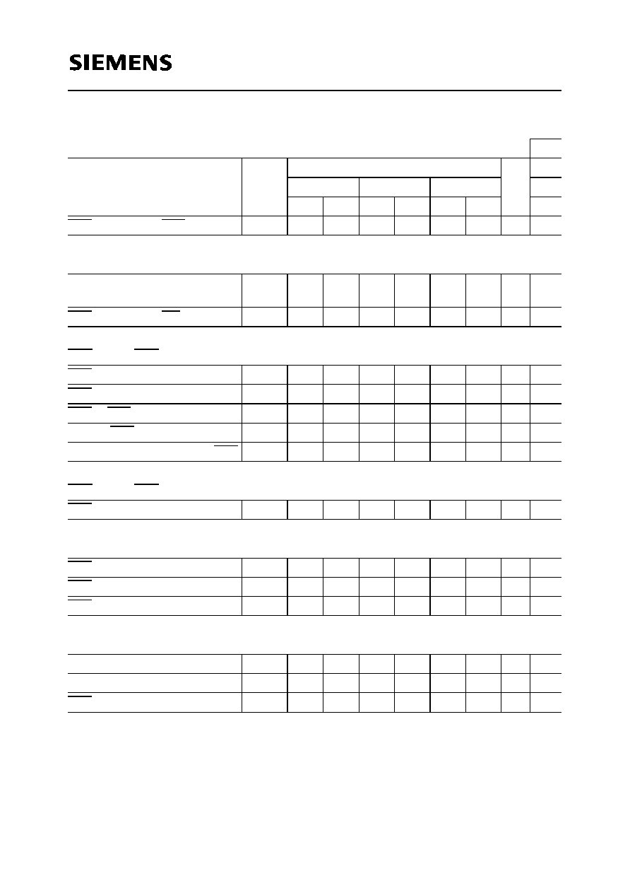
Capacitance
T
A
= 0 to 70 ∞C,
V
CC
= 3.3 V
±
0.3V,
f
= 1 MHz
Parameter
Symbol
Limit Values
Unit
min.
max.
Input capacitance (A0 to A10, A11)
C
I1
≠
5
pF
Input capacitance (RAS, CAS, WE, OE)
C
I2
≠
7
pF
I/O capacitance (I/O1 - I/O4)
C
IO
≠
7
pF
DC Characteristics (values in brackets for HYB3117405)
T
A
= 0 to 70 ∞C,
V
SS
= 0 V,
V
CC
= 3.3 V
±
0.3 V,
t
T
= 2 ns
Parameter
Symbol
Limit Values
Unit Test
Condition
min.
max.
Semiconductor Group
8
HYB 3116(7)405BJ/BT(L) -50/-60/-70
3.3V 4Mx4-DRAM
AC Characteristics 5)6)
16E
T
A
= 0 to 70 ∞C,
V
CC
= 5 V
±
10 %,
t
T
= 2 ns
Parameter
Symbol
Limit Values
Unit
Note
-50
-60
-70
min.
max. min.
max. min.
max.
common parameters
Random read or write cycle time
t
RC
84
≠
104
≠
124
≠
ns
RAS precharge time
t
RP
30
≠
40
≠
50
≠
ns
RAS pulse width
t
RAS
50
10k
60
10k
70
10k
ns
CAS pulse width
t
CAS
8
10k
10
10k
12
10k
ns
Row address setup time
t
ASR
0
≠
0
≠
0
≠
ns
Row address hold time
t
RAH
8
≠
10
≠
10
≠
ns
Column address setup time
t
ASC
0
≠
0
≠
0
≠
ns
Column address hold time
t
CAH
8
≠
10
≠
12
≠
ns
RAS to CAS delay time
t
RCD
12
37
14
45
14
53
ns
RAS to column address delay
t
RAD
10
25
12
30
12
35
ns
RAS hold time
t
RSH
13
15
≠
17
≠
ns
CAS hold time
t
CSH
40
50
≠
60
≠
ns
CAS to RAS precharge time
t
CRP
5
≠
5
≠
5
≠
ns
Transition time (rise and fall)
t
T
1
50
1
50
1
50
ns
7
Refresh period for HYB5116405
t
REF
≠
64
≠
64
≠
64
ms
Refresh period for HYB5117405
t
REF
≠
32
≠
32
≠
32
ms
Refresh period for L-version
t
REF
≠
256
≠
256
≠
256
ms
Read Cycle
Access time from RAS
t
RAC
≠
50
≠
60
≠
70
ns
8, 9
Access time from CAS
t
CAC
≠
13
≠
15
≠
17
ns
8, 9
Access time from column address
t
AA
≠
25
≠
30
≠
35
ns
8,10
OE access time
t
OEA
≠
13
≠
15
≠
17
ns
Column address to RAS lead time
t
RAL
25
≠
30
≠
35
≠
ns
Read command setup time
t
RCS
0
≠
0
≠
0
≠
ns
Read command hold time
t
RCH
0
≠
0
≠
0
≠
ns
11
Read command hold time
referenced to RAS
t
RRH
0
≠
0
≠
0
≠
ns
11
CAS to output in low-Z
t
CLZ
0
≠
0
≠
0
≠
ns
8

Semiconductor Group
9
HYB 3116(7)405BJ/BT(L) -50/-60/-70
3.3V 4Mx4-DRAM
Output buffer turn-off delay
t
OFF
0
13
0
15
0
17
ns
12
Output turn-off delay from OE
t
OEZ
0
13
0
15
0
17
ns
12
Data to CAS low delay
t
DZC
0
≠
0
≠
0
≠
ns
13
Data to OE low delay
t
DZO
0
≠
0
≠
0
≠
ns
13
CAS high to data delay
t
CDD
10
≠
13
≠
15
≠
ns
14
OE high to data delay
t
ODD
10
≠
13 ≠
15
≠
ns
14
Write Cycle
Write command hold time
t
WCH
8
≠
10
≠
10
≠
ns
Write command pulse width
t
WP
8
≠
10
≠
10
≠
ns
Write command setup time
t
WCS
0
≠
0
≠
0
≠
ns
15
Write command to RAS lead time
t
RWL
13
≠
15
≠
17
≠
ns
Write command to CAS lead time
t
CWL
13
≠
15
≠
17
≠
ns
Data setup time
t
DS
0
≠
0
≠
0
≠
ns
16
Data hold time
t
DH
8
≠
10
≠
12
≠
ns
16
Read-modify-Write Cycle
Read-write cycle time
t
RWC
113
≠
138
≠
162
≠
ns
RAS to WE delay time
t
RWD
64
≠
77
≠
89
≠
ns
15
CAS to WE delay time
t
CWD
27
≠
32
≠
36
≠
ns
15
Column address to WE delay time
t
AWD
39
≠
47
≠
54
≠
ns
15
OE command hold time
t
OEH
10
≠
13
≠
15
≠
ns
Hyper Page Mode (EDO) Cycle
Hyper page mode (EDO) cycle
time
t
HPC
20
≠
25
≠
30
≠
ns
CAS precharge time
t
CP
8
≠
10
≠
10
≠
ns
Access time from CAS precharge
t
CPA
≠
27
≠
32
≠
37
ns
7
Output data hold time
t
COH
5
≠
5
≠
5
≠
ns
RAS pulse width in EDO mode
t
RAS
50
200k
60
200k 70
200k
ns
AC Characteristics
(cont'd)
5)6)
16E
T
A
= 0 to 70 ∞C,
V
CC
= 5 V
±
10 %,
t
T
= 2 ns
Parameter
Symbol
Limit Values
Unit
Note
-50
-60
-70
min.
max. min.
max. min.
max.
Semiconductor Group
10
HYB 3116(7)405BJ/BT(L) -50/-60/-70
3.3V 4Mx4-DRAM
CAS precharge to RAS Delay
t
RHPC
27
≠
32
≠
37
≠
ns
Hyper Page Mode (EDO) Read-modify-Write Cycle
Hyper page mode (EDO) read-
write cycle time
t
PRWC
58
≠
68
≠
77
≠
ns
CAS precharge to WE
t
CPWD
41
≠
49
≠
56
≠
ns
CAS-before-RAS Refresh Cycle
CAS setup time
t
CSR
10
≠
10
≠
10
≠
ns
CAS hold time
t
CHR
10
≠
10
≠
10
≠
ns
RAS to CAS precharge time
t
RPC
5
≠
5
≠
5
≠
ns
Write to RAS precharge time
t
WRP
10
≠
10
≠
10
≠
ns
Write hold time referenced to RAS
t
WRH
10
≠
10
≠
10
≠
ns
CAS-before-RAS Counter Test Cycle
CAS precharge time
t
CPT
35
≠
40
≠
40
≠
ns
Self Refresh Cycle
RAS pulse width
t
RASS
100k
_
100k
_
100k
_
ns
17
RAS precharge
t
RPS
95
_
110
_
130
_
ns
17
CAS hold time
t
CHS
-50
_
-50
_
-50
_
ns
17
Test Mode
Write command setup time
t
WTS
10
≠
10
≠
10
≠
ns
Write command hold time
t
WTH
10
≠
10
≠
10
≠
ns
CAS hold time
t
CHRT
30
≠
30
≠
30
≠
ns
AC Characteristics
(cont'd)
5)6)
16E
T
A
= 0 to 70 ∞C,
V
CC
= 5 V
±
10 %,
t
T
= 2 ns
Parameter
Symbol
Limit Values
Unit
Note
-50
-60
-70
min.
max. min.
max. min.
max.
Semiconductor Group
11
HYB 3116(7)405BJ/BT(L) -50/-60/-70
3.3V 4Mx4-DRAM
Notes:
1) All voltages are referenced to
V
SS
.
2)
I
CC1
,
I
CC3
,
I
CC4
and
I
CC6
depend on cycle rate.
3)
I
CC1
and
I
CC4
depend on output loading. Specified values are obtained with the output open.
4) Address can be changed once or less while RAS = Vil. In case of ICC4 it can be changed once or less during
a hyper page mode (EDO) cycle
5) An initial pause of 200
µ
s is required after power-up followed by 8 RAS cycles of which at least one cycle has
to be a refresh cycle, before proper device operation is achieved. In case of using the internal refresh counter,
a minimum of 8 CAS-before-RAS initialization cycles instead of 8 RAS cycles are required.
6) AC measurements assume
t
T
= 2 ns.
7)
V
I
H
(min.)
and
V
I
L (max.)
are reference levels for measuring timing of input signals. Transition times are also
measured between
V
I
H
and
V
I
L
.
8) Measured with the specified current load and 100 pF at Vol = 0.8 V and Voh = 2.0 V. Access time is determined
by the latter of tRAC, tCAC, tAA,tCPA, tOEA . tCAC is measured from tristate.
9) Operation within the
t
RCD (max.)
limit ensures that
t
RAC (max.)
can be met.
t
RCD (max.)
is specified as a reference point
only. If
t
RCD
is greater than the specified
t
RCD (max.)
limit, then access time is controlled by
t
CAC
.
10) Operation within the
t
RAD (max.
)
limit ensures that
t
RAC (max.)
can be met.
t
RAD (max.)
is specified as a reference point
only. If
t
RAD
is greater than the specified
t
RAD (max.)
limit, then access time is controlled by
t
AA
.
11) Either
t
RCH
or
t
RRH
must be satisfied for a read cycle.
12)
t
OFF (max.)
,
t
OEZ (max.)
define the time at which the output achieves the open-circuit conditions and are not
referenced to output voltage levels.
t
OFF
is referenced from the rising edge of RAS or CAS, whichever occurs
last.
13) Either
t
DZC
or
t
DZO
must be satisfied.
14) Either
t
CDD
or
t
ODD
must be satisfied.
15)
t
WCS
,
t
RWD
,
t
CWD
and
t
AWD
are not restrictive operating parameters. They are included in the data sheet as
electrical characteristics only. If
t
WCS
>
t
WCS (min.)
, the cycle is an early write cycle and data out pin will remain
open-circuit (high impedance) through the entire cycle; if
t
RWD
>
t
RWD (min.)
,
t
CWD
>
t
CWD (min.)
and
t
AWD
>
t
AWD (min.)
,
the cycle is a read-write cycle and I/O will contain data read from the selected cells. If neither of the above
sets of conditions is satisfied, the condition of I/O (at access time) is indeterminate.
16) These parameters are referenced to the CAS leading edge in early write cycles and to the WE leading edge
in read-write cycles.
17)When using Self Refresh mode, the following refresh operations must be performed to ensure proper DRAM
operation:
If row addresses are being refreshed on an evenly distributed manner over the refresh interval using CBR
refresh cycles, then only one CBR cycle must be performed immediately after exit from Self Refresh.
If row addresses are being refreshed in any other manner (ROR - Distributed/Burst; or CBR-Burst) over the
refresh interval, then a full set of row refreshes must be performed immediately before entry to and immediately
after exit from Self Refresh

Semiconductor Group
12
HYB 3116(7)405BJ/BT(L) -50/-60/-70
3.3V 4Mx4-DRAM
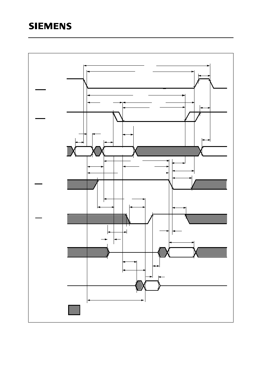
Waveforms
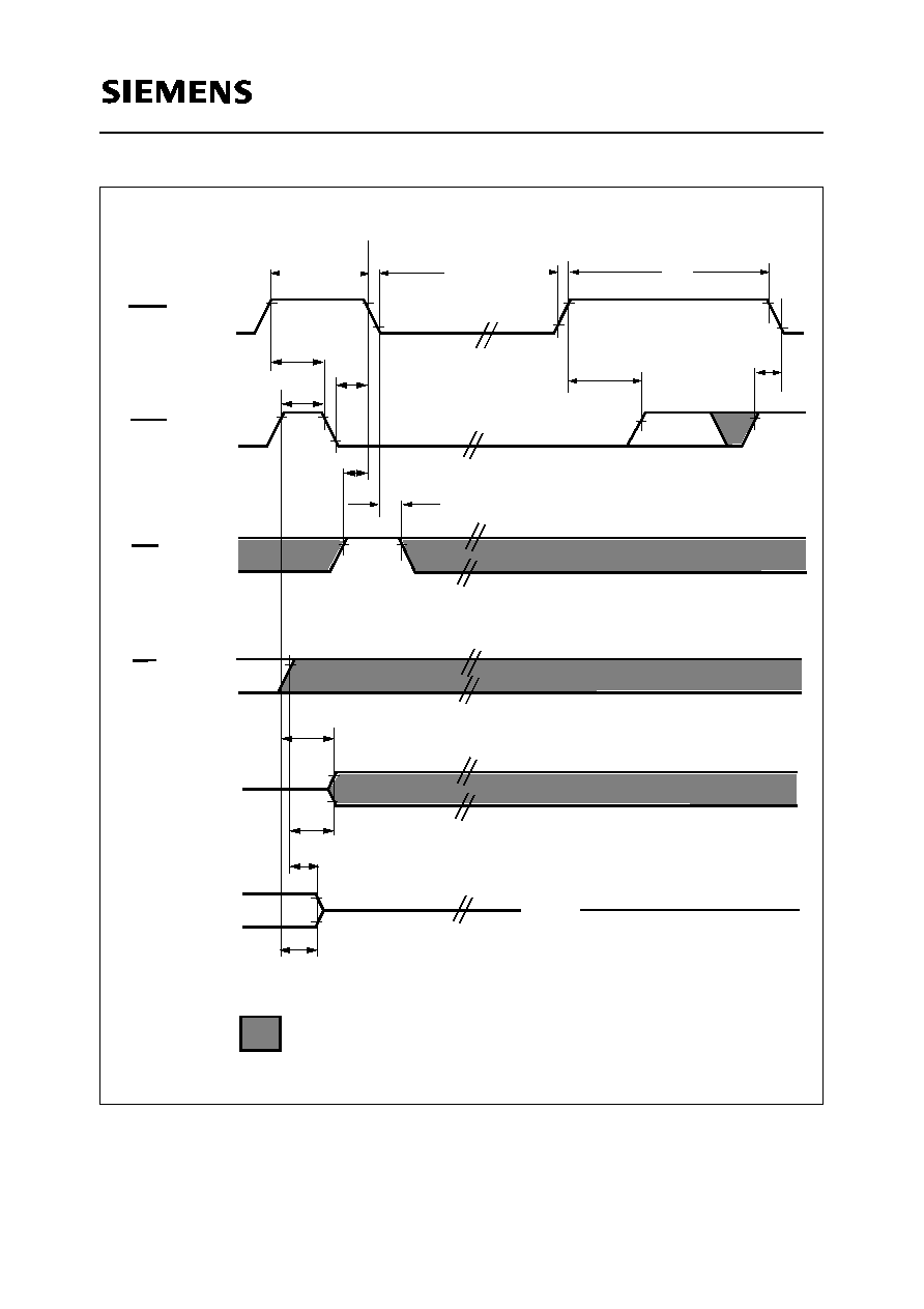
Read Cycle
Row
Column
Row
Valid Data Out
RAS
CAS
Address
WE
OE
I/O
(Inputs)
I/O
(Outputs)
V
IH
V
IL
V
IH
V
IL
V
IH
V
IL
V
IH
V
IL
V
IH
V
IL
V
IH
V
IL
V
OH
V
OL
t
RAS
t
RC
t
CSH
t
RAD
t
CAS
t
RP
t
RAH
t
CRP
t
RSH
t
RCD
t
RAL
t
ASR
t
CAH
t
ASC
t
ASR
t
RCH
t
RRH
t
RCS
t
AA
t
OEA
t
CLZ
t
CAC
t
OEZ
t
ODD
t
CDD
t
OFF
t
DZC
t
DZO
t
RAC
Hi Z
Hi Z
"H" or "L"
WL1

Semiconductor Group
13
HYB 3116(7)405BJ/BT(L) -50/-60/-70
3.3V 4Mx4-DRAM
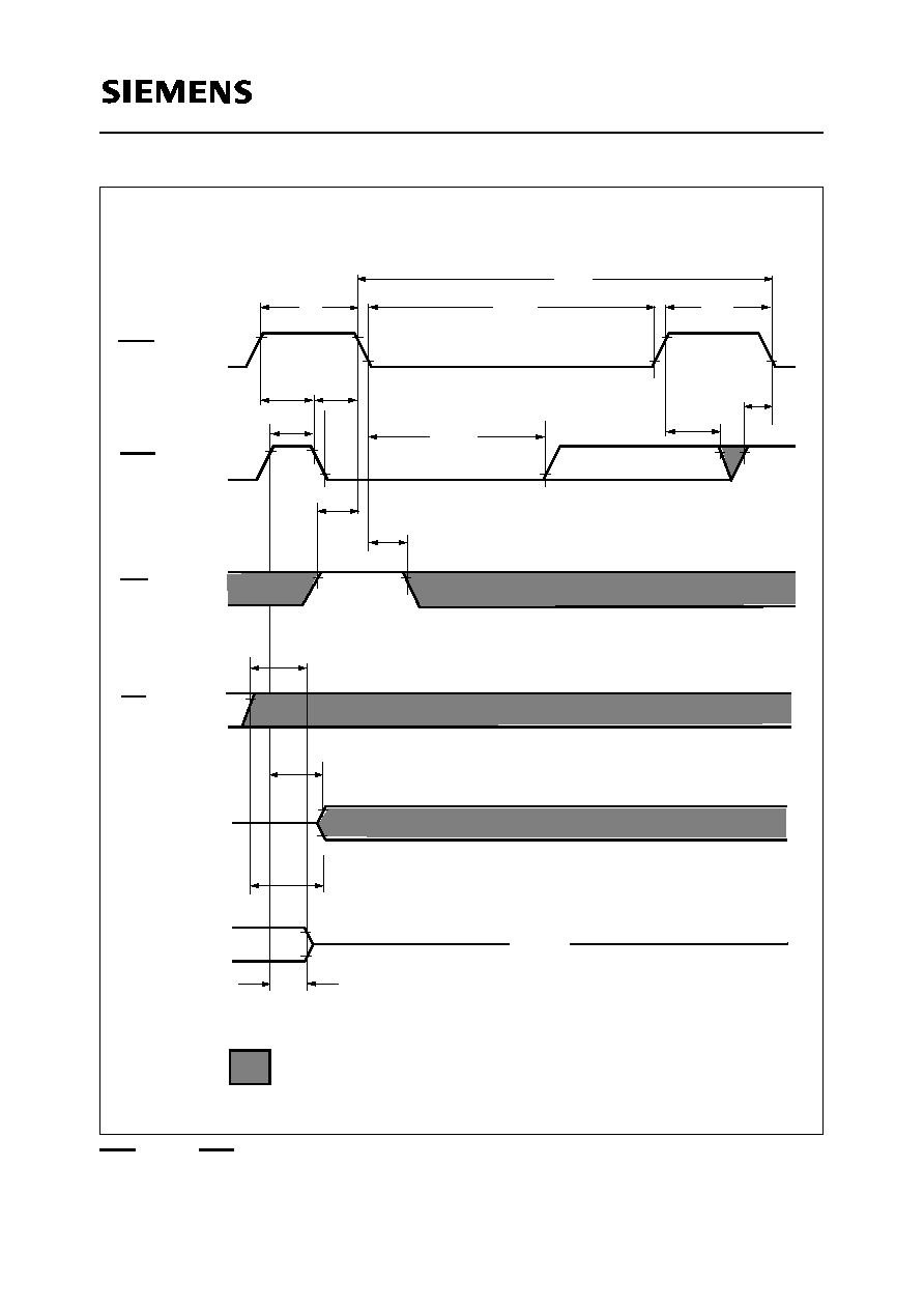
Write Cycle (Early Write)
RAS
CAS
Address
WE
OE
I/O
(Inputs)
I/O
(Outputs)
V
IH
V
IL
V
IH
V
IL
V
IH
V
IL
V
IH
V
IL
V
IH
V
IL
V
IH
V
IL
V
OH
V
OL
.
t
RAS
t
RC
t
CSH
t
RAD
t
CAS
t
RP
t
CRP
t
RSH
t
RCD
t
RAL
t
ASR
t
CAH
t
ASR
t
CWL
t
RWL
t
WP
t
ASC
t
WCH
Valid Data In
t
DS
t
DH
Hi Z
Column
Row
Row
t
RAH
t
WCS
"H" or "L"
WL2

Semiconductor Group
14
HYB 3116(7)405BJ/BT(L) -50/-60/-70
3.3V 4Mx4-DRAM
Write Cycle (OE Controlled Write)
Valid Data
t
RWL
t
WP
t
OEH
t
ODD
t
CWL
t
DZO
t
OEA
t
CLZ
t
DS
t
OEZ
t
DH
t
RC
V
IH
V
IL
Row
t
DZC
"H" or "L"
Hi-Z
Hi-Z
Column
Row
t
ASC
t
RAD
t
RAL
t
CAH
t
RAH
RAS
CAS
Address
WE
OE
I/O
(Inputs)
I/O
(Outputs)
V
IH
V
IL
V
IH
V
IL
V
IH
V
IL
V
IH
V
IL
V
IH
V
IL
V
OH
V
OL
.
t
RAS
t
CSH
t
CAS
t
RP
t
CRP
t
RSH
t
RCD
t
ASR
t
ASR
WL3
Semiconductor Group
15
HYB 3116(7)405BJ/BT(L) -50/-60/-70
3.3V 4Mx4-DRAM
Read-Write (Read-Modify-Write) Cycle
Row
Row
t
CSH
t
CAS
t
CRP
t
RWC
t
AWD
t
ASR
t
RP
t
RAS
t
RAH
t
CAH
I/O
(Outputs)
V
OH
V
OL
V
IH
V
IL
V
IH
V
IL
I/O
(Inputs)
OE
WE
V
IH
V
IL
t
ASR
Column
t
RCD
t
DH
t
RSH
t
RAD
t
CWD
t
OEH
t
RWD
t
RWL
t
CWL
t
CLZ
t
WP
t
RCS
t
AA
t
OEA
t
DS
t
DZC
t
DZO
t
ODD
t
CAC
t
OEZ
Valid
Data in
Data
Out
t
RAC
"H" or "L"
t
ASC
V
IH
V
IL
V
IH
V
IL
RAS
CAS
Address
V
IH
V
IL
WL4
Semiconductor Group
16
HYB 3116(7)405BJ/BT(L) -50/-60/-70
3.3V 4Mx4-DRAM
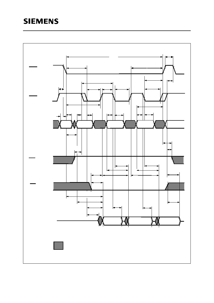
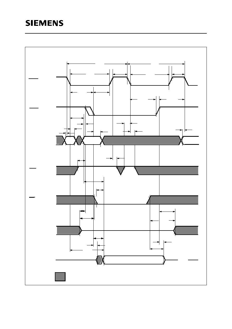
Hyper Page Mode (EDO) Read Cycle
t
RP
t
RSH
t
CAS
t
CAS
t
CP
t
CRP
t
RAL
t
CAH
t
CAH
t
ASC
t
CSH
t
CAS
t
RCD
t
RAH
t
ASR
Column 2
Row
Data Out
RAS
I/O
WE
Address
CAS
V
IH
V
IL
V
IH
V
IL
V
IH
V
IL
VIH
V
IL
V
IH
V
IL
"H" or "L"
V
OH
V
OL
OE
t
RAS
t
CRP
t
ASC
t
HPC
t
CAH
t
RAD
t
RHCP
t
ASC
t
RCS
t
RRH
t
RCH
(Output)
t
RAC
t
AA
t
CAC
t
CLZ
t
OEA
t
OES
t
COH
t
CAC
t
AA
t
CPA
Data Out
Column N
Column 1
Data Out
t
OEZ
t
OFF
t
CAC
t
AA
t
CPA
1
2
t
COH
N
WL5
Semiconductor Group
17
HYB 3116(7)405BJ/BT(L) -50/-60/-70
3.3V 4Mx4-DRAM
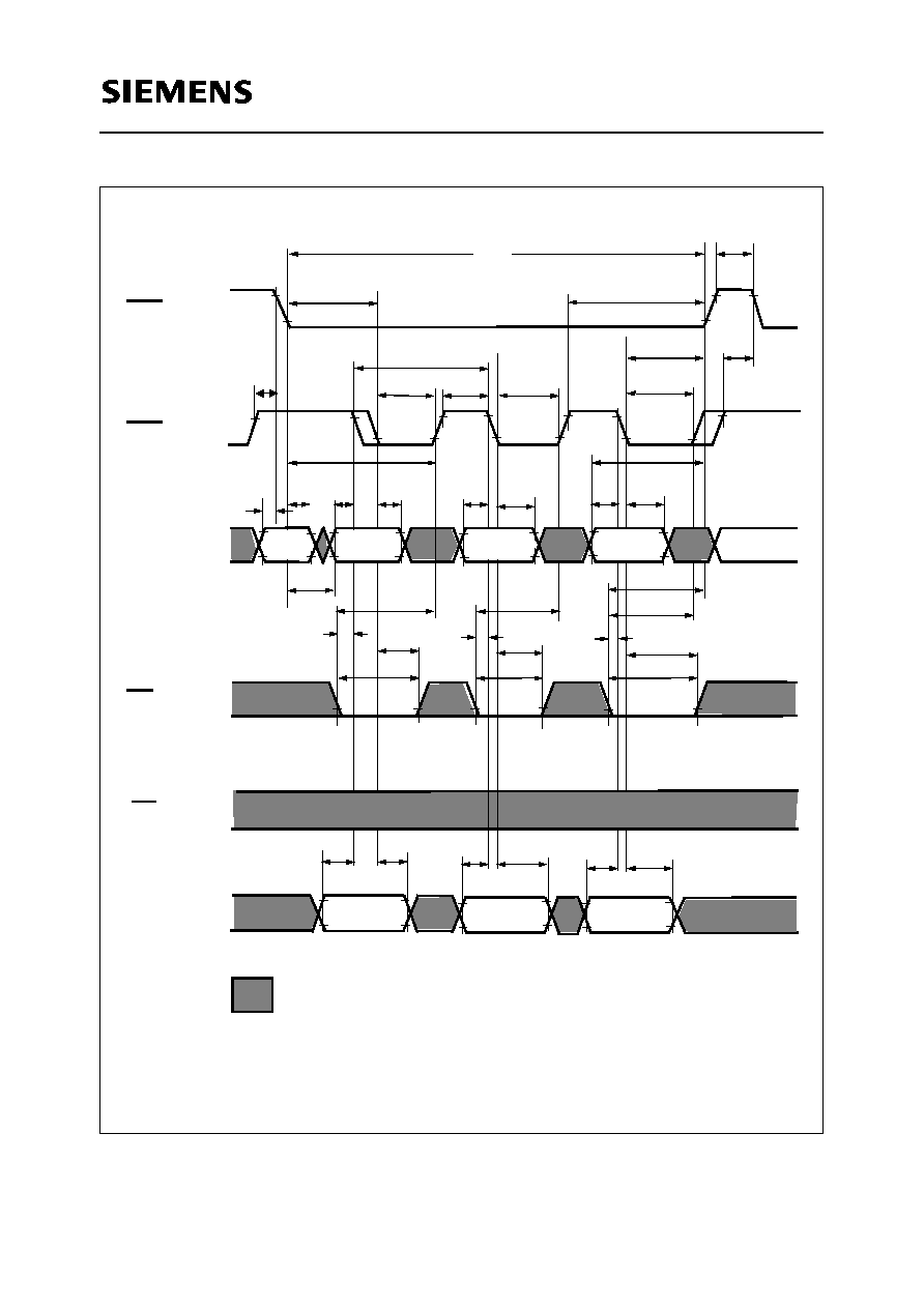
Hyper Page Mode (EDO) Early Write Cycle
t
RP
t
RSH
t
CAS
t
CAS
t
CP
t
CRP
t
RAL
t
CAH
t
CAH
t
ASC
t
CWL
t
WCS
t
WP
t
WCH
t
CSH
t
CAS
t
RCD
t
RAH
t
ASR
t
DH
t
DS
t
DH
t
DS
Column 1
Column 2
Row
Addr
Data In N
Data In 2
Data In 1
Column N
RAS
I/O (Input)
WE
Address
CAS
V
IH
V
IL
V
IH
V
IL
V
IH
V
IL
VIH
V
IL
V
IH
V
IL
"H" or "L"
V
OH
V
OL
OE
t
RAS
t
CRP
t
ASC
t
CWL
t
WCS
t
WP
t
WCH
t
CWL
t
WCS
t
WP
t
WCH
t
RWL
t
DH
t
DS
t
HPC
t
CAH
t
RAD
t
RHCP
t
ASC
WL8
Semiconductor Group
18
HYB 3116(7)405BJ/BT(L) -50/-60/-70
3.3V 4Mx4-DRAM
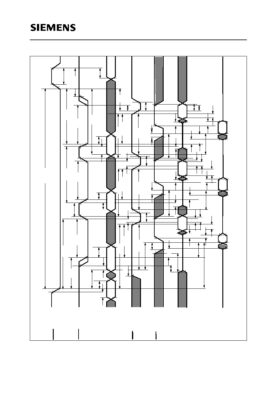
Hyper Page Mode (EDO) Late Write and Read-Modify-Write Cycle
t
CA
H
t
CP
t
DZC
t
DZO
t
RA
C
t
CA
C
t
CL
Z
t
RC
S
t
AA
t
OE
A
t
RC
D
t
RA
D
t
RA
H
t
AS
R
t
ASC
t
CA
S
t
CA
S
t
PRW
C
t
CW
D
t
CAH
t
AS
C
t
CAS
t
RSH
t
RP
t
CR
P
t
AS
R
t
CA
H
t
ASC
t
RAL
t
CW
D
t
RW
D
t
CW
L
t
CW
L
t
CW
D
t
AW
D
t
AW
D
t
WP
t
WP
t
CW
L
t
RW
L
t
AW
D
t
WP
t
ODD
t
OE
H
t
DH
t
DS
t
CP
A
t
OE
Z
t
CL
Z
t
DZ
C
t
AA
t
CA
C
t
OE
A
t
DS
t
OE
Z
t
DH
t
OE
H
t
AA
t
OD
D
t
DZC
t
CP
A
t
OE
A
t
CL
Z
t
DS
t
DH
t
OE
H
t
ODD
RAS
V
IH
V
IL
CAS
V
IH
V
IL
V
IH
V
IL
V
IH
V
IL
V
IH
V
IL
V
IH
V
IL
V
OH
V OL
WE
OE
Address
I/O
(Inputs)
I/O
(Outputs)
D
a
ta
I
n
D
a
ta
In
Da
t
a
I
n
Da
t
a
Ou
t
Ou
t
Da
t
a
Da
t
a
Ou
t
Ro
w
Co
l
u
mn
Co
l
u
m
n
Ro
w
t
RA
SP
t
CSH
Co
l
u
mn
t
CP
W
D
t
CP
W
D
WL17

Semiconductor Group
19
HYB 3116(7)405BJ/BT(L) -50/-60/-70
3.3V 4Mx4-DRAM
RAS-Only Refresh Cycle
t
CRP
t
RAH
t
RP
t
RAS
t
RC
t
ASR
t
ASR
t
RPC
V
IH
V
IL
V
IH
V
IL
V
IH
V
IL
V
OH
V
OL
Row
Row
HI-Z
Address
RAS
CAS
I/O
(Outputs)
"H" or "L"
WL9
Semiconductor Group
20
HYB 3116(7)405BJ/BT(L) -50/-60/-70
3.3V 4Mx4-DRAM
Self Refresh
t
RPS
t
RASS
t
RP
t
CRP
t
CP
t
RPC
t
WRH
t
WRP
t
CSR
t
OFF
t
OEZ
t
CDD
t
ODD
V
IH
V
IL
V
IH
V
IL
V
IH
V
IL
V
IH
V
IL
V
IH
V
IL
HI-Z
"H" or "L"
RAS
I/O
(Outputs)
I/O
(Inputs)
OE
WE
CAS
V
OH
V
OL
t
CHS
WL13
Semiconductor Group
21
HYB 3116(7)405BJ/BT(L) -50/-60/-70
3.3V 4Mx4-DRAM
CAS-Before-RAS Refresh Cycle
t
RP
t
RAS
t
RP
t
RC
t
CRP
t
CP
t
RPC
t
CHR
t
WRH
t
WRP
t
CSR
t
RPC
t
OFF
t
OEZ
t
CDD
t
ODD
V
IH
V
IL
V
IH
V
IL
V
IH
V
IL
V
IH
V
IL
V
IH
V
IL
HI-Z
"H" or "L"
RAS
I/O
(Outputs)
I/O
(Inputs)
OE
WE
CAS
V
OH
V
OL
WL10
Semiconductor Group
22
HYB 3116(7)405BJ/BT(L) -50/-60/-70
3.3V 4Mx4-DRAM
Hidden Refresh Cycle (Read)
RAS
I/O
(Outputs)
I/O
(Inputs)
OE
WE
Address
CAS
t
RC
t
RC
t
RAS
t
RAS
t
RP
t
RP
t
CRP
t
CHR
t
RAD
t
CAH
t
ASC
t
RAH
t
ASR
t
ASR
t
RCS
t
RRH
t
AA
t
DZC
t
DZO
t
CAC
t
RAC
t
CLZ
t
OEZ
t
OFF
t
ODD
t
CDD
t
RCD
t
RSH
t
OEA
V
IH
V
IL
V
IH
V
IL
V
IH
V
IL
V
IH
V
IL
V
IH
V
IL
V
IH
V
IL
t
WRP
t
WRH
"H" or "L"
Valid Data Out
Row
Column
Row
HI-Z
V
OH
V
OL
WL11

Semiconductor Group
23
HYB 3116(7)405BJ/BT(L) -50/-60/-70
3.3V 4Mx4-DRAM
Hidden Refresh Cycle (Early Write)
RAS
I/O
(Output)
I/O
(Input)
WE
Address
V
IH
V
IL
V
IH
V
IL
V
IH
V
IL
CAS
V
IH
V
IL
V
IH
V
IL
"H" or "L"
t
RC
t
RAS
t
RCD
t
RSH
t
RAD
t
CAH
t
WCS
t
WCH
t
WP
t
ASR
t
RAH
t
DS
t
DH
t
ASR
t
CRP
t
CHR
t
RP
t
RAS
t
RC
t
RP
t
ASC
Row
Row
Valid Data
HI-Z
Column
V
OH
V
OL
t
WRP
t
WRH
WL12

Semiconductor Group
24
HYB 3116(7)405BJ/BT(L) -50/-60/-70
3.3V 4Mx4-DRAM
CAS-Before-RAS Refresh Counter Test Cycle
t
CSR
t
ASR
t
ASC
t
CHR
t
CP
t
WRP
t
RAL
t
CAH
t
RSH
t
RP
t
RAS
t
CAS
t
RCS
t
CDD
t
CAC
t
AA
t
WRH
t
OEA
t
ODD
t
CLZ
t
DZC
t
DZO
t
OEZ
t
OFF
t
RWL
t
CWL
t
WCH
t
WCS
t
WRH
t
WRP
t
DS
t
DH
V
IH
V
IL
V
IH
V IL
V
IH
V IL
VOH
VOL
V
IH
V IL
V
IH
V IL
V
IH
V IL
V
IH
V IL
V
IH
V IL
V
IH
V IL
V
IH
V IL
RAS
I/O
(Inputs)
OE
WE
Address
CAS
I/O
(Outputs)
I/O
(Outputs)
I/O
(Inputs)
WE
OE
Column
Row
Data Out
Data In
HI-Z
Read Cycle:
Write Cycle:
t
RRH
t
RCH

Semiconductor Group
25
HYB 3116(7)405BJ/BT(L) -50/-60/-70
3.3V 4Mx4-DRAM
Test Mode Entry
t
RC
t
RAS
t
RP
t
RPC
t
CRP
t
CHR
t
WTH
t
RPC
t
RP
t
CP
t
CSR
t
WTS
t
CDD
t
OFF
t
OEZ
t
ODD
I/O
(Outputs)
V
OH
V
OL
V
IH
V
IL
V
IH
V
IL
I/O
(Inputs)
OE
WE
V
IH
V
IL
CAS
RAS
V
IH
V
IL
V
IH
V
IL
"H" or "L"
HI-Z
Address
t
RAH
t
ASR
V
IH
V
IL
Row
WL15
HI-Z

Semiconductor Group
26
HYB 3116(7)405BJ/BT(L) -50/-60/-70
3.3V 4Mx4-DRAM
Package Outlines
Plastic Package P-SOJ-26/24-1 (300 mil)
(Small Outline J-leads, SMD)
1) Does not include plastic or metal protrusion of 0.15 max per side
Index Marking
GPJ05628
24x
0.2
M
-0.1
-0.2
0.6
0.1
1)
Index Marking
9.22
13
1
14
26
7.62
+0.12
0.4
1.27
17.27
0.2
-+
0.13
-+
-0.25
GPX05857