
Semiconductor Group
1
4M
◊
72-Bit Dynamic RAM Module
(ECC - Module )
HYM 724000GS-50/-60
HYM 724010GS-50/-60
Preliminary Information
∑
4 194 304 words by 72-bit ECC - mode organization
∑
Fast access and cycle time
50 ns access time
90 ns cycle time (-50 version)
60 ns access time
110 ns cycle time (-60 version)
∑
Fast page mode capability with
35 ns cycle time (-50 version)
40 ns cycle time (-60 version)
∑
Single + 5 V (
±
10 %) supply
∑
Low power dissipation
max. 9900 mW active (-50 version)
max. 8910 mW active (-60 version)
CMOS ≠ 165
mW
standby
TTL
≠ 275 mW standby
∑
CAS-before-RAS refresh, RAS-only-refresh
∑
18 decoupling capacitors mounted on substrate
∑
All inputs, outputs and clock fully TTL compatible
∑
4 Byte interleave enabled, Dual Address inputs (A0/B0)
∑
Buffered inputs excepts RAS and DQ
∑
168 pin, dual read-out, Single in-Line Memory Module
∑
Utilizes eighteen 4M
◊
4 -DRAMs in TSOPII-packages
and four BiCMOS 8-bit buffers/line drivers 74ABT244
∑
Two versions : HYM 724000GS with TSOPII-components (4.06 mm thickness)
HYM 724010GS with SOJ-components (8.89 mm thickness)
∑
4096 refresh cycles / 64 ms with 12 / 10 addressing
∑
Gold contact pad
∑
double sided module with 25.35 mm (1000 mil) height
1
11.95

Semiconductor Group
2
HYM724000/10GS-50/-60
4M x 72 ECC- Module
The HYM 724000/10GS-60/-70 is a 32 MByte DRAM module organized as 4 194 430 words by 72-
bit in a 168-pin, dual read-out, single-in-line package comprising eighteen HYB 5116400BT/BJ
4M
◊
4 DRAMs in 300 mil wide TSOPII or SOJ- packages mounted together with eighteen 0.2
µ
F
ceramic decoupling capacitors on a PC board. All inputs except RAS and DQ are buffered by using
four BiCMOS 8-bit buffers/line drivers.
Each HYB 5116400BT/BJ is described in the data sheet and is fully electrically tested and
processed according to Siemens standard quality procedure prior to module assembly. After
assembly onto the board, a further set of electrical tests is performed.
The density and speed of the module can be detected by the use of presence detect pins.
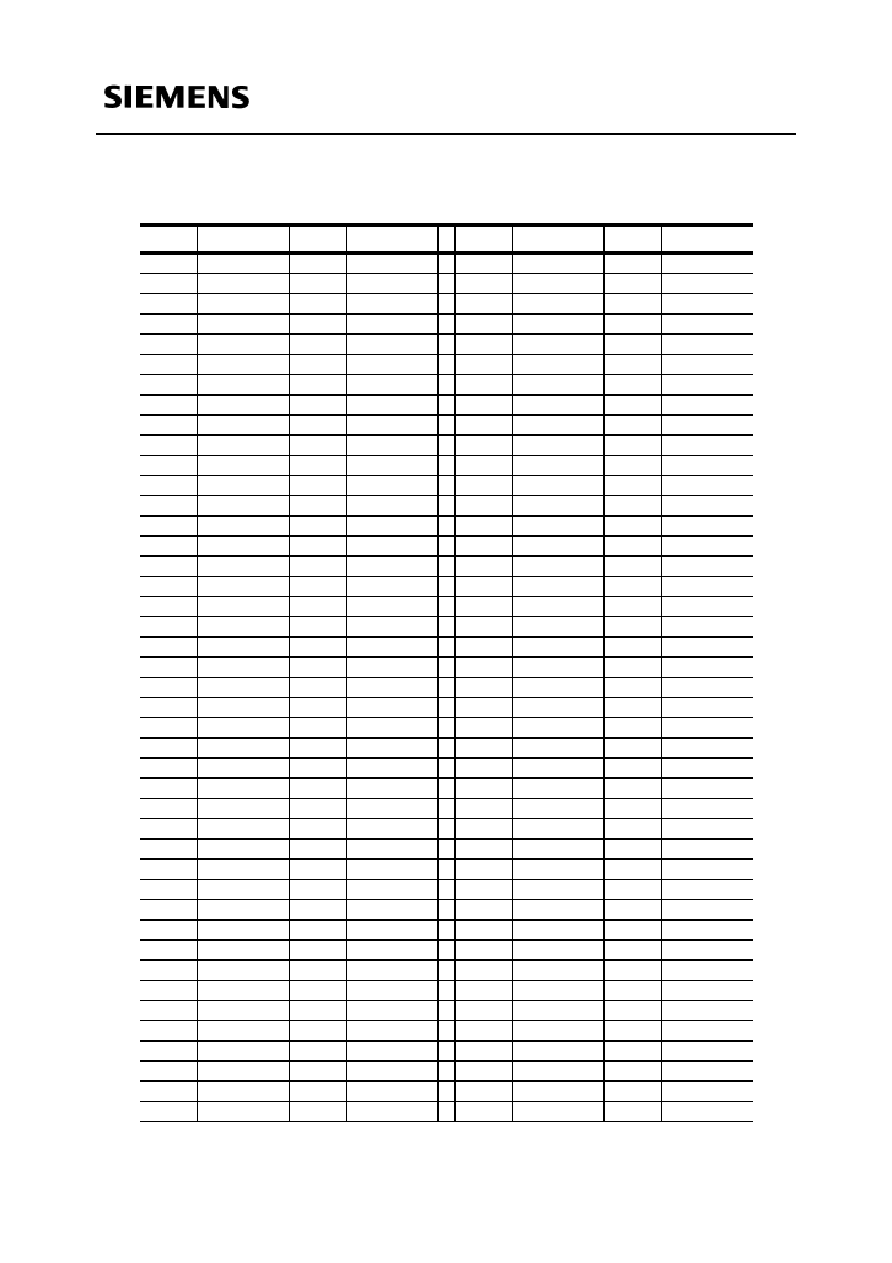
Ordering Information
Pin Names
Presence-Detect and ID-pin Truth Table:
Note: 1 = High Level ( Driver Output) , 0 = Low Level (Driver Output) for PDE active ( ground) . For PDE at a high
level all PD terminal are in tri-state.
Type
Ordering Code
Package
Descriptions
HYM 724000GS-50
L-DIM-168-6
50ns DRAM module
HYM 724000GS-60
Q67100-Q2075
L-DIM-168-6
60ns DRAM module
HYM 724010GS-50
L-DIM-168-6
50ns DRAM module
HYM 724010GS-60
Q67100-Q2076
L-DIM-168-6
60ns DRAM module
A0-A11,B0
Address Input
DQ0 - DQ71
Data Input/Output
RAS0, RAS2
Row Address Strobe
CAS0 , CAS2
Column Address Strobe
WE0, WE2
Read / Write Input
OE0, OE2
Output Enable
Vcc
Power (+5 Volt)
Vss
Ground
PD1 - PD8
Presence Detect Pins
PDE
Presence Detect Enable
ID0 , ID1
ID indentification bit
N.C.
No Connection
Module
ID0
ID1
PD1
PD2
PD3
PD4
PD5
PD6
PD7
PD8
HYM 724000GS-50
Vss
Vss
1
1
0
1
0
0
0
0
HYM 724000GS-60
Vss
Vss
1
1
0
1
0
1
1
0
Semiconductor Group
3
HYM724000/10GS-50/-60
4M x 72 ECC- Module
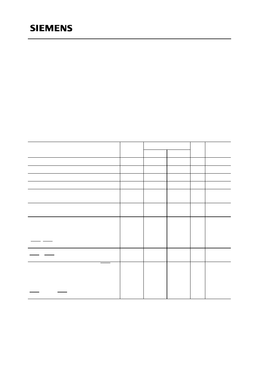
Pin Configuration
PIN #
Symbol
PIN #
Symbol
PIN #
Symbol
PIN #
Symbol
1
VSS
43
VSS
85
VSS
127
VSS
2
DQ0
44
OE2
86
DQ36
128
NC
3
DQ1
45
RAS2
87
DQ37
129
NC
4
DQ2
46
CAS4
88
DQ38
130
NC
5
DQ3
47
NC
89
DQ39
131
NC
6
VCC
48
WE2
90
VCC
132
PDE
7
DQ4
49
VCC
91
DQ40
133
VCC
8
DQ5
50
NC
92
DQ41
134
NC
9
DQ6
51
NC
93
DQ42
135
NC
10
DQ7
52
DQ18
94
DQ43
136
DQ54
11
DQ8
53
DQ19
95
DQ44
137
DQ55
12
VSS
54
VSS
96
VSS
138
VSS
13
DQ9
55
DQ20
97
DQ45
139
DQ56
14
DQ10
56
DQ21
98
DQ46
140
DQ57
15
DQ11
57
DQ22
99
DQ47
141
DQ58
16
DQ12
58
DQ23
100
DQ48
142
DQ59
17
DQ13
59
VCC
101
DQ49
143
VCC
18
VCC
60
DQ24
102
VCC
144
DQ60
19
DQ14
61
NC
103
DQ50
145
NC
20
DQ15
62
NC
104
DQ51
146
NC
21
DQ16
63
NC
105
DQ52
147
NC
22
DQ17
64
NC
106
DQ53
148
NC
23
VSS
65
DQ25
107
VSS
149
DQ61
24
NC
66
DQ26
108
NC
150
DQ62
25
NC
67
DQ27
109
NC
151
DQ63
26
VCC
68
VSS
110
VCC
152
VSS
27
WE0
69
DQ28
111
NC
153
DQ64
28
CAS0
70
DQ29
112
NC
154
DQ65
29
NC
71
DQ30
113
NC
155
DQ66
30
RAS0
72
DQ31
114
NC
156
DQ67
31
OE0
73
VCC
115
NC
157
VCC
32
VSS
74
DQ32
116
VSS
158
DQ68
33
A0
75
DQ33
117
A1
159
DQ69
34
A2
76
DQ34
118
A3
160
DQ70
35
A4
77
DQ35
119
A5
161
DQ71
36
A6
78
VSS
120
A7
162
VSS
37
A8
79
PD1
121
A9
163
PD2
38
A10
80
PD3
122
A11
164
PD4
39
NC
81
PD5
123
NC
165
PD6
40
VCC
82
PD7
124
VCC
166
PD8
41
NC
83
ID0 (VSS)
125
NC
167
ID1 (VSS)
42
NC
84
VCC
126
B0
168
VCC

Semiconductor Group
4
HYM724000/10GS-50/-60
4M x 72 ECC- Module
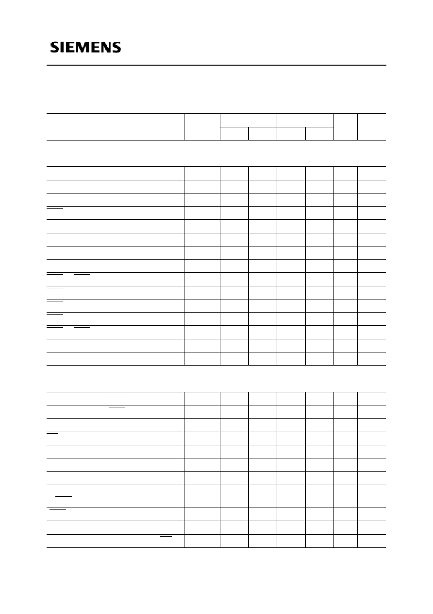
Block Diagram
I/O1-I/O4
D0
I/O1-I/O4
D1
I/O1-I/O4
D2
I/O1-I/O4
D3
I/O1-I/O4
D4
I/O1-I/O4
D5
I/O1-I/O4
D6
I/O1-I/O4
D7
I/O1-I/O4
D8
I/O1-I/O4
D9
I/O1-I/O4
D10
I/O1-I/O4
D11
I/O1-I/O4
D12
I/O1-I/O4
D13
I/O1-I/O4
D14
I/O1-I/O4
D15
I/O1-I/O4
D16
I/O1-I/O4
D17
D0 - D8
D9 - D17
D0 - D17
DQ0-DQ3
DQ4-DQ7
RAS0
CAS0
WE0
OE0
DQ8-DQ11
DQ12-DQ15
DQ16-DQ19
DQ20-DQ23
DQ24-DQ27
DQ28-DQ31
DQ32-DQ35
DQ36-DQ39
DQ40-DQ43
RAS2
CAS4
WE2
OE2
DQ44-DQ47
DQ48-DQ51
DQ52-DQ55
DQ56-DQ59
DQ60-DQ63
DQ64-DQ67
DQ68-DQ71
A0
B0
A1-A11
Vcc
Vss
D0-D17, buffers
Vcc or Vss
PD1-PD8
PDE
Semiconductor Group
5
HYM724000/10GS-50/-60
4M x 72 ECC- Module
Absolute Maximum Ratings
Operating temperature range ......................................................................................... 0 to + 70 ∞C
Storage temperature range...................................................................................... ≠ 55 to + 125 ∞C
Input/output voltage ............................................................................... -0.5 to min (Vcc+0.5, 7.0) V
Power supply voltage...................................................................................................... ≠ 1 to + 7 V
Power dissipation................................................................................................................ 12,60 W
Data out current (short circuit) ................................................................................................ 50 mA
Note:
Stresses above those listed under "Absolute Maximum Ratings" may cause permanent
damage to the device. Exposure to absolute maximum rating conditions for extended periods
may affect device reliability.
DC Characteristics
T
A
= 0 to 70 ∞C;
V
CC
= 5 V
±
10 %
Parameter
Symbol
Limit Values
Unit
Test
Condition
min.
max.
Input high voltage
V
IH
2.4
5.5
V
1)
Input low voltage
V
IL
≠ 1.0
0.8
V
1)
Output high voltage (
I
OUT
= ≠ 5 mA)
V
OH
2.4
≠
V
1)
Output low voltage (
I
OUT
= 4.2 mA)
V
OL
≠
0.4
V
1)
Input leakage current
(0 V <
V
IN
< 6.5 V, all other pins = 0 V)
I
I(L)
≠ 10
10
µ
A
1)
Output leakage current
(DO is disabled, 0 V <
V
OUT
< 5.5 V)
I
O(L)
≠ 10
10
µ
A
1)
Average
V
CC
supply current:
-50 version
-60 version
(RAS, CAS, address cycling,
t
RC
=
t
RC
min.)
I
CC1
≠
≠
1800
1620
mA
mA
2) 3) 4)
Standby
V
CC
supply current
(RAS = CAS =
V
IH
)
I
CC2
≠
50
mA
≠
Average
V
CC
supply current during RAS
only refresh cycles:
-50 version
-60 version
(RAS cycling, CAS =
V
IH
, t
RC
=
t
RC
min.)
I
CC3
≠
≠
1800
16
mA
mA
2) 4)

Semiconductor Group
6
HYM724000/10GS-50/-60
4M x 72 ECC- Module
DC Characteristics (cont'd)
1)
Capacitance
T
A
= 0 to 70 ∞C;
V
CC
= 5 V
±
10 %;
f
= 1 MHz
Parameter
Symbol
Limit Values
Unit
Test
Condition
min.
max.
Average
V
CC
supply current during fast
page mode:
-50 version
-60 version
(RAS =
V
IL,
CAS, address cycling
t
PC
=
t
PC
min.)
I
CC4
≠
≠
≠
720
630
mA
mA
2) 3) 4)
Standby
V
CC
supply current
(RAS = CAS =
V
CC
≠ 0.2 V)
I
CC5
≠
30
mA
≠
Average
V
CC
supply current during
CAS-before-RAS refresh mode:
-50 version
-60 version
(RAS, CAS cycling
, t
RC
=
t
RC
min.)
I
CC6
≠
≠
1800
1620
mA
mA
2) 4)
Parameter
Symbol
Limit Values
Unit
min.
max.
Input capacitance (A0 to A11,B0)
C
I1
≠
10
pF
Input capacitance (RAS0, RAS2)
C
I2
≠
50
pF
Input capacitance (CAS0-CAS7)
C
I3
≠
15
pF
Input capacitance (WE0,WE2,OE0,OE2)
C
I4
≠
15
pF
I/O capacitance (DQ0-DQ71)
C
IO1
≠
15
pF
Semiconductor Group
7
HYM724000/10GS-50/-60
4M x 72 ECC- Module
AC Characteristics (note: 5,6,7,8)
T
A
= 0 to 70 ∞C,
V
CC
= 5.0
±
10 %
Parameter
Symbol
-50
-60
Unit
Note
min.
max.
min.
max.
common parameters
Random read or write cycle time
t
RC
90
≠
110
≠
ns
RAS precharge time
t
RP
30
≠
40
≠
ns
RAS pulse width
t
RAS
50
100k
60
100k
ns
CAS pulse width
t
CAS
13
100k
15
100k
ns
Row address setup time
t
ASR
5
≠
5
≠
ns
9
Row address hold time
t
RAH
8
≠
8
≠
ns
10
Column address setup time
t
ASC
2
≠
2
≠
ns
11
Column address hold time
t
CAH
15
≠
15
≠
ns
9
RAS to CAS delay time
t
RCD
16
32
18
40
12
RAS to column address delay time
t
RAD
11
20
13
25
ns
12
RAS hold time
t
RSH
18
≠
20
≠
ns
9
CAS hold time
t
CSH
48
≠
58
≠
ns
10
CAS to RAS precharge time
t
CRP
10
≠
10
≠
ns
9
Transition time (rise and fall)
t
T
3
30
3
30
ns
7
Refresh period
t
REF
≠
64
≠
64
ms
Read Cycle
Access time from RAS
t
RAC
≠
50
≠
60
ns
13,14
Access time from CAS
t
CAC
≠
18
≠
20
ns
9,13,14
Access time from column address
t
AA
≠
30
≠
35
ns
9,13, 15
OE access time
t
OEA
≠
18
≠
20
ns
9,13
Column address to RAS lead time
t
RAL
30
≠
35
≠
ns
9
Read command setup time
t
RCS
2
≠
2
≠
ns
11
Read command hold time
t
RCH
2
≠
2
≠
ns
11,16
Read command hold time referenced
to RAS
t
RRH
0
≠
0
≠
ns
16
CAS to output in low-Z
t
CLZ
2
≠
2
≠
ns
11,13
Output buffer turn-off delay
t
OFF
≠
18
≠
20
ns
9,17
Output buffer turn-off delay from OE
t
OEZ
≠
18
≠
20
ns
9,17

Semiconductor Group
8
HYM724000/10GS-50/-60
4M x 72 ECC- Module
CAS delay time from Din
t
DZC
0
≠
0
≠
ns
18
Data to OE low delay
t
DZO
0
≠
0
≠
ns
18
CAS high to data delay
t
CDD
18
≠
20
≠
ns
9,19
OE high to data delay
t
ODD
18
≠
20
≠
ns
9,19
Write Cycle
Write command hold time
t
WCH
13
≠
15
≠
ns
9
Write command pulse width
t
WP
8
≠
10
≠
ns
Write command setup time
t
WCS
2
≠
2
≠
ns
11,20
Write command to RAS lead time
t
RWL
18
≠
20
≠
ns
9
Write command to CAS lead time
t
CWL
13
≠
15
≠
ns
Data setup time
t
DS
-2
≠
-2
≠
ns
10,21
Data hold time
t
DH
15
≠
15
≠
ns
9,21
Read-Modify-Write Cycle
Read-write cycle time
t
RWC
131
≠
155
≠
ns
9
RAS to WE delay time
t
RWD
70
≠
82
≠
ns
11,21
CAS to WE delay time
t
CWD
33
≠
37
≠
ns
11,21
Column address to WE delay time
t
AWD
45
≠
52
≠
ns
11,21
OE command hold time
t
OEH
11
≠
13
≠
ns
10
Fast Page Mode Cycle
Fast page mode cycle time
t
PC
35
≠
40
≠
ns
CAS precharge time
t
CP
10
≠
10
≠
ns
Access time from CAS precharge
t
CPA
≠
35
≠
40
ns
9,13
RAS pulse width
t
RAS
50
200k 60
200k
ns
CAS precharge to RAS Delay
t
RHCP
35
≠
40
≠
ns
9
AC Characteristics (cont'd)(note: 5,6,7,8)
T
A
= 0 to 70 ∞C,
V
CC
= 5.0
±
10 %
Parameter
Symbol
-50
-60
Unit
Note
min.
max.
min.
max.
Semiconductor Group
9
HYM724000/10GS-50/-60
4M x 72 ECC- Module
Fast Page Mode Read-Modify-Write
Cycle
Fast page mode read-write cycle time
t
PRWC
73
≠
82
≠
ns
11
CAS precharge to WE
t
CPWD
50
≠
57
≠
ns
11,21
CAS-before-RAS Refresh Cycle
CAS setup time
t
CSR
7
≠
7
≠
ns
11
CAS hold time
t
CHR
8
≠
8
≠
ns
10
RAS to CAS precharge time
t
RPC
5
≠
5
≠
ns
Write to RAS precharge time
t
WRP
12
≠
12
≠
ns
11
Write hold time referenced to RAS
t
WRH
8
≠
8
≠
ns
10
Presence Detect Read Cycle
PDE to valid presence detect data
t
PD
≠
10
≠
10
ns
PDE inactive to presence detects
inactive
t
PDOFF
0
10
0
10
ns
AC Characteristics (cont'd)(note: 5,6,7,8)
T
A
= 0 to 70 ∞C,
V
CC
= 5.0
±
10 %
Parameter
Symbol
-50
-60
Unit
Note
min.
max.
min.
max.
Semiconductor Group
10
HYM724000/10GS-50/-60
4M x 72 ECC- Module
Notes:
1) All voltages are referenced to VSS.
2) ICC1, ICC3, ICC4 and ICC6 and ICC7 depend on cycle rate.
3) ICC1 and ICC4 depend on output loading. Specified values are measured with the output open.
4) Address can be changed once or less while RAS = Vil.In the case of ICC4 it can be changed once or less
during a fast page mode cycle ( tpc).
5) An initial pause of 100
µ
s is required after power-up followed by 8 RAS-only-refresh cycles, before proper
device operation is achieved. In case of using internal refresh counter, a minimum of 8 CAS-before-RAS
initialization cycles instead of 8 RAS cycles are required.
6) AC measurements assume tT = 5 ns.
7) VIH (min.) and VIL (max.) are reference levels for measuring timing of input signals. Also, transition times are
measured between VIH and VIL.
8) The specified timings include buffer, loading and skew delay adders: 2ns minimum, 5ns (CAS, WE, OE,
addresses) maximum delay, no pulse shrinkage to the DRAM device timings. The data and RAS signals are
not buffered, which preserves the DRAMs access specification of 50ns and 60ns.
9) A +5ns timing skew from the DRAM to the module resulted from the addition of line drivers.
10) A -2ns timing skew from the DRAM to the module resulted from the addition of line drivers.
11) A +2ns timing skew from the DRAM to the module resulted from the addition of line drivers.
12) A -2ns (min.) and a -5ns (max.) timing skew from the DRAM to the module resulted from the addition of line
drivers.
13) Measured with the specified current load and 100 pF at Voh = 2.4 V and Vol = 0.4 V.
14) Operation within the tRCD (max.) limit ensures that tRAC (max.) can be met. tRCD (max.) is specified as a
reference point only: If tRCD is greater than the specified tRCD (max.) limit, then access time is controlled by
tCAC.
15) Operation within the tRAD (max.) limit ensures that tRAC (max.) can be met. tRAD (max.) is specified as a
reference point only: If tRAD is greater than the specified tRAD (max.) limit, then access time is controlled by
tAA.
16) Either tRCH or tRRH must be satisfied for a read cycle.
17) tOFF (max.) and tOEZ (max.) define the time at which the outputs achieve the open-circuit condition and are
not referenced to output voltage levels.
18) Either tDZC or tDZO must be satisfied.
19) Either tCDD or tODD must be satisfied.
20) tWCS, tRWD, tCWD, tAWD and tCPWD are not restrictive operating parameters. They are included in the data
sheet as electrical characteristics only. If tWCS > tWCS (min.), the cycle is an early write cycle and the I/O pin
will remain open-circuit (high impedance) through the entire cycle; if tRWD > tRWD (min.), tCWD > tCWD
(min.), tAWD > tAWD (min.) and tCPWD > tCPWD (min.) , the cycle is a read-write cycle and I/O pins will
contain data read from the selected cells. If neither of the above sets of conditions is satisfied, the condition
of the I/O pins (at access time) is indeterminate.
21) These parameters are referenced to CAS leading edge in early write cycles and to WE leading edge in Read-
Modify-Write cycles.

Semiconductor Group
11
HYM724000/10GS-50/-60
4M x 72 ECC- Module
L-DIM-168-6
Module package
(dual read-out, single in-line memory module)
133,35
1
84
17,78
Detail of Contacts
1.27
2.54 min
0.25 max
+/- 0.05
25,40
10 11
40
41
85
95 96
* )
preliminary drawing
168
3,0
127,35
1.0
124
125
DM168-6.WMF
4Mx72 5V
*) 9 mm thickness for modules assembled with SOJ-devices
4mm thickness for modules assembled with TSOPII-devices