
Semiconductor Group 1 5.96
∑
1 048 576 words by 4-bit organization
∑
0 to 70 ∞C operating temperature
∑
Hyper Page Mode - EDO
∑
Performance:
∑
Single + 5 V (
±
10 %) supply
∑
Low power dissipation
max. 660 mW active (-50 version)
max. 605 mW active (-60 version)
max. 550 mW active (-70 version)
∑
Standby power dissipation:
11 mW max.standby (TTL)
5.5 mW max.standby (CMOS)
1.1 mW max.standby (CMOS) for Low Power Version
∑
Read, write, read-modify write, CAS-before-RAS refresh, RAS-only refresh,
hidden refresh and test mode capability
∑
All inputs and outputs TTL-compatible
∑
1024 refresh cycles / 16 ms
∑
1024 refresh cycles / 128 ms for Low Power Version
∑
Plastic Packages: P-SOJ-26/20-5 with 300 mil width
-50
-60
-70
t
RAC
RAS access time
50
60
70
ns
t
CAC
CAS access time
13
15
20
ns
t
AA
Access time from address
25
30
35
ns
t
RC
Read/Write cycle time
89
104
124
ns
t
HPC
Hyper page mode (EDO)
cycle time
20
25
30
ns
1M x 4-Bit Dynamic RAM
(Hyper Page Mode (EDO) version)
Preliminary Information
HYB 514405BJ/BJL-50/-60/-70

Semiconductor Group
2
HYB 514405BJ/BLJ-50/-60/-70
1M x 4 EDO - DRAM
The HYB 514405BJ is the new generation dynamic RAM organized as 1 048 576 words by 4-bit.
The HYB 514405BJ utilizes CMOS silicon gate process as well as advances circuit techniques to
provide wide operation margins, both internally and for the system user. Multiplexed address inputs
permit the HYB 514405BJ to be packed in a standard plastic P-SOJ-26/20 package. This package
size provides high system bit densities and is compatible with commonly used automatic testing and
insertion equipment. System oriented feature include single + 5 V (
±
10 %) power supply, direct
interfacing with high performance logic device families.
Ordering Information
Type
Ordering Code
Package
Descriptions
HYB 514405BJ-50
Q67100-Q2116
P-SOJ-26/20-5
EDO-DRAM
(access time 50 ns)
HYB 514405BJ-60
Q67100-Q2118
P-SOJ-26/20-5
EDO-DRAM
(access time 60 ns)
HYB 514405BJ-70
Q67100-Q2120
P-SOJ-26/20-5
EDO-DRAM
(access time 70 ns)
HYB 514405BJL-50
on request
P-SOJ-26/20-5
Low Power EDO-DRAM
(access time 50 ns)
HYB 514405BJL-60
on request
P-SOJ-26/20-5
Low Power EDO-DRAM
(access time 60 ns)
HYB 514405BJL-70
on request
P-SOJ-26/20-5
Low Power EDO-DRAM
(access time 70 ns)

Semiconductor Group
3
HYB 514405BJ/BJL-50/-60/-70
1M x 4 EDO - DRAM
Pin Configuration
(top view)
Pin Names
A0-A9
Address Input
RAS
Row Address Strobe
CAS
Column Address Strobe
WE
Read/Write Input
OE
Output Enable
I/
O1 -
I/
O4
Data Input/Output
V
CC
Power Supply (+ 5 V)
V
SS
Ground (0 V)
N.C.
No Connection
P-SOJ-26/20-5

Semiconductor Group
4
HYB 514405BJ/BLJ-50/-60/-70
1M x 4 EDO - DRAM
Block Diagram

Semiconductor Group
5
HYB 514405BJ/BJL-50/-60/-70
1M x 4 EDO - DRAM
Absolute Maximum Ratings
Operating temperature range ............................................................................................0 to 70 ∞C
Storage temperature range......................................................................................≠ 55 to + 150 ∞C
Input/output voltage ........................................................................................................ ≠ 1 to + 7 V
Power Supply voltage ..................................................................................................... ≠ 1 to + 7 V
Data out current (short circuit) ................................................................................................ 50 mA
Note:
Stresses above those listed under "Absolute Maximum Ratings" may cause permanent
damage of the device. Exposure to absolute maximum rating conditions for extended periods
may affect device reliability.
DC Characteristics
T
A
= 0 to 70 ∞C,
V
SS
= 0 V,
V
CC
= 5 V
±
10 %,
t
T
= 2 ns
Parameter
Symbol
Limit Values
Unit Test
Condition
min.
max.
Input high voltage
V
ih
2.4
V
CC
+ 0.5 V
1)
Input low voltage
V
il
≠ 1.0
0.8
V
1)
Output high voltage (
I
OUT
= ≠ 5 mA)
V
oh
2.4
≠
V
1)
Output low voltage (
I
OUT
= 4.2 mA)
V
ol
≠
0.4
V
1)
Input leakage current, any input
(0 V <
V
in
< 7, all other input = 0 V)
I
I(L)
≠ 10
10
µ
A
1)
Output leakage current
(DO is disabled, 0 <
V
OUT
<
V
CC
)
I
o(L)
≠ 10
10
µ
A
1)
Average
V
CC
supply current
-50 version
-60 version
-70 version
I
CC1
≠
≠
≠
120
110
100
mA
2) 3)4)
Standby
V
CC
supply current
(RAS = CAS = WE =
V
ih
)
I
CC2
≠
2
mA
≠
Average
V
CC
supply current during RAS-only
refresh cycles
-50 version
-60 version
-70 version
I
CC3
≠
≠
≠
120
110
100
mA
2)4)
Average
V
CC
supply current during hyper page
mode(EDO) operation
-50 version
-60 version
-70 version
I
CC4
≠
≠
≠
100
90
80
mA
2) 3)4)
Standby
V
CC
supply current
(RAS = CAS = WE =
V
CC
≠ 0.2 V)
I
CC5
≠
1
200
mA
µ
A
1)
L-version

Semiconductor Group
6
HYB 514405BJ/BLJ-50/-60/-70
1M x 4 EDO - DRAM
Average
V
CC
supply current during
CAS before RAS refresh mode
-50 version
-60 version
-70 version
I
CC6
≠
≠
≠
120
110
100
mA
2)4)
For Low Power Version only:
Battery backup current (average power supply
current in battery backup mode):
(CAS = CAS before RAS cycling or 0.2 V,
WE =
V
CC
≠ 0.2 V or 0.2 V,
A0 to A10 =
V
CC
≠ 0.2 V or 0.2 V;
D
I
=
V
CC
≠ 0.2 V or 0.2 V or open,
t
RC
= 125
µ
s,
t
RAS
=
t
RAS
min = 1
µ
s)
I
CC7
≠
250
µ
A
≠
AC Characteristics
5)6)
T
A
= 0 to 70 ∞C,
V
CC
= 5 V
±
10 %,
t
T
= 2 ns
Parameter
Symbol
Limit Values
Unit
Note
-50
-60
-70
min.
max. min.
max. min.
max.
Common Parameters
Random read or write cycle time
t
RC
89
≠
104
≠
124
≠
ns
RAS precharge time
t
RP
35
≠
40
≠
50
≠
ns
RAS pulse width
t
RAS
50
10k
60
10k
70
10k
ns
CAS pulse width
t
CAS
8
10k
10
10k
12
10k
ns
Row address setup time
t
ASR
0
≠
0
≠
0
≠
ns
Row address hold time
t
RAH
8
≠
10
≠
10
≠
ns
Column address setup time
t
ASC
0
≠
0
≠
0
≠
ns
Column address hold time
t
CAH
8
≠
10
≠
12
≠
ns
RAS to CAS delay time
t
RCD
12
37
14
45
14
53
ns
RAS to column address delay
time
t
RAD
10
25
12
30
12
35
ns
RAS hold time
t
RSH
13
15
≠
17
≠
ns
DC Characteristics (cont'd)
T
A
= 0 to 70 ∞C,
V
SS
= 0 V,
V
CC
= 5 V
±
10 %,
t
T
= 2 ns
Parameter
Symbol
Limit Values
Unit Test
Condition
min.
max.

Semiconductor Group
7
HYB 514405BJ/BJL-50/-60/-70
1M x 4 EDO - DRAM
CAS hold time
t
CSH
50
60
≠
70
≠
ns
CAS to RAS precharge time
t
CRP
5
≠
5
≠
5
≠
ns
Transition time (rise and fall)
t
T
1
50
1
50
1
50
ns
7
Refresh period
t
REF
≠
16
≠
16
≠
16
ms
Refresh period for L-version
t
REF
≠
128
≠
128
≠
128
ms
Read Cycle
Access time from RAS
t
RAC
≠
50
≠
60
≠
70
ns
8, 9
Access time from CAS
t
CAC
≠
13
≠
15
≠
17
ns
8, 9
Access time from column
address
t
AA
≠
25
≠
30
≠
35
ns
8,10
OE access time
t
OEA
≠
13
≠
15
≠
17
ns
Column address to RAS lead
time
t
RAL
25
≠
30
≠
35
≠
ns
Read command setup time
t
RCS
0
≠
0
≠
0
≠
ns
Read command hold time
t
RCH
0
≠
0
≠
0
≠
ns
11
Read command hold time
referenced to RAS
t
RRH
0
≠
0
≠
0
≠
ns
11
CAS to output in low-Z
t
CLZ
0
≠
0
≠
0
≠
ns
8
Output buffer turn-off delay
t
OFF
0
13
0
15
0
17
ns
12
Output buffer turn-off delay from
OE
t
OEZ
0
13
0
15
0
17
ns
12
Data to CAS low delay
t
DZC
0
≠
0
≠
0
≠
ns
13
Data to OE low delay
t
DZO
0
≠
0
≠
0
≠
ns
13
CAS high to data delay
t
CDD
10
≠
13
≠
15
≠
ns
14
OE high to data delay
t
ODD
10
≠
13
≠
15
≠
ns
14
Write Cycle
Write command hold time
t
WCH
8
≠
10
≠
10
≠
ns
Write command pulse width
t
WP
8
≠
10
≠
10
≠
ns
Write command setup time
t
WCS
0
≠
0
≠
0
≠
ns
15
AC Characteristics (cont'd)
5)6)
T
A
= 0 to 70 ∞C,
V
CC
= 5 V
±
10 %,
t
T
= 2 ns
Parameter
Symbol
Limit Values
Unit
Note
-50
-60
-70
min.
max. min.
max. min.
max.

Semiconductor Group
8
HYB 514405BJ/BLJ-50/-60/-70
1M x 4 EDO - DRAM
Write command to RAS lead time
t
RWL
13
≠
15
≠
17
≠
ns
Write command to CAS lead time
t
CWL
13
≠
15
≠
17
≠
ns
Data setup time
t
DS
0
≠
0
≠
0
≠
ns
16
Data hold time
t
DH
8
≠
10
≠
12
≠
ns
16
Read-modify-Write Cycle
Read-write cycle time
t
RWC
118
≠
138
≠
162
≠
ns
RAS to WE delay time
t
RWD
64
≠
77
≠
89
≠
ns
15
CAS to WE delay time
t
CWD
27
≠
32
≠
36
≠
ns
15
Column address to WE delay
time
t
AWD
39
≠
47
≠
54
≠
ns
15
OE command hold time
t
OEH
10
≠
13
≠
15
≠
ns
Hyper Page Mode (EDO) Cycle
Hyper page mode (EDO) cycle
time
t
HPC
20
≠
25
≠
30
≠
ns
CAS precharge time
t
CP
8
≠
10
≠
10
≠
ns
Access time from CAS
precharge
t
CPA
≠
27
≠
32
≠
37
ns
7
Output data hold time
t
COH
5
≠
5
≠
5
≠
ns
RAS pulse width in hyper page
mode
t
RAS
50
200k
60
200k
70
200k
ns
CAS precharge to RAS Delay
t
RHCP
27
≠
32
≠
37
≠
ns
Hyper Page Mode (EDO) Read-
modify-Write Cycle
Hyper page mode (EDO) read-
write cycle time
t
PRWC
58
≠
68
≠
77
≠
ns
CAS precharge to WE
t
CPWD
41
≠
49
≠
56
≠
ns
AC Characteristics (cont'd)
5)6)
T
A
= 0 to 70 ∞C,
V
CC
= 5 V
±
10 %,
t
T
= 2 ns
Parameter
Symbol
Limit Values
Unit
Note
-50
-60
-70
min.
max. min.
max. min.
max.

Semiconductor Group
9
HYB 514405BJ/BJL-50/-60/-70
1M x 4 EDO - DRAM
CAS before RAS Refresh Cycle
CAS setup time
t
CSR
10
≠
10
≠
10
≠
ns
CAS hold time
t
CHR
10
≠
10
≠
10
≠
ns
RAS to CAS precharge time
t
RPC
5
≠
5
≠
5
≠
ns
Write to RAS precharge time
t
WRP
10
≠
10
≠
10
≠
ns
Write hold time referenced to
RAS
t
WRH
10
≠
10
≠
10
≠
ns
CAS-before-RAS Counter Test
Cycle
CAS precharge time (CAS-
before-RAS counter test cycle)
t
CPT
35
≠
40
≠
40
≠
ns
Test Mode
Write command setup time
t
WTS
10
≠
10
≠
10
≠
ns
Write command hold time
t
WTH
10
≠
10
≠
10
≠
ns
Capacitance
T
A
= 0 to 70 ∞C;
V
CC
= 5 V
±
10 %;
f
= 1 MHz
Parameter
Symbol
Limit Values
Unit
min.
max.
Input capacitance (A0 to A9)
C
i1
≠
5
pF
Input capacitance (RAS, CAS, WE,OE)
C
i2
≠
7
pF
Output capacitance (
I
O1 to
I
O4)
C
io
≠
7
pF
AC Characteristics (cont'd)
5)6)
T
A
= 0 to 70 ∞C,
V
CC
= 5 V
±
10 %,
t
T
= 2 ns
Parameter
Symbol
Limit Values
Unit
Note
-50
-60
-70
min.
max. min.
max. min.
max.

Semiconductor Group
10
HYB 514405BJ/BLJ-50/-60/-70
1M x 4 EDO - DRAM
Notes:
1) All voltages are referenced to
V
SS
.
2)
I
CC1
,
I
CC3
,
I
CC4
and
I
CC6
depend on cycle rate.
3)
I
CC1
and
I
CC4
depend on output loading. Specified values are obtained with the output open.
4) Address can be changed once or less while RAS =
V
il
. In case of
I
CC4
it can be changed once or less during
a hyper page mode (EDO) cycle
5) An initial pause of 200
µ
s is required after power-up followed by 8 RAS cycles of which at least one cycle has
to be a refresh cycle, before proper device operation is achieved. In case of using the internal refresh counter,
a minimum of 8 CAS-before-RAS initialization cycles instead of 8 RAS cycles are required.
6) AC measurements assume
t
T
= 2 ns.
7)
V
IH
(min.)
and
V
IL (max.)
are reference levels for measuring timing of input signals. Transition times are also
measured between
V
IH
and
V
IL
.
8) Measured with the specified current load and 100 pF at
V
ol
= 0.8 V and
V
oh
= 2.0 V. Access time is determined
by the latter of
t
RAC
,
t
CAC
,
t
AA
,
t
CPA
,
t
OEA
.
t
CAC
is measured from tristate.
9) Operation within the
t
RCD (max.)
limit ensures that
t
RAC (max.)
can be met.
t
RCD (max.)
is specified as a reference point
only. If
t
RCD
is greater than the specified
t
RCD (max.)
limit, then access time is controlled by
t
CAC
.
10) Operation within the
t
RAD (max.
)
limit ensures that
t
RAC (max.)
can be met.
t
RAD (max.)
is specified as a reference point
only. If
t
RAD
is greater than the specified
t
RAD (max.)
limit, then access time is controlled by
t
AA
.
11) Either
t
RCH
or
t
RRH
must be satisfied for a read cycle.
12)
t
OFF (max.)
,
t
OEZ (max.)
define the time at which the output achieves the open-circuit conditions and are not
referenced to output voltage levels.
t
OFF
is referenced from the rising edge of RAS or CAS, whichever occurs
last.
13) Either
t
DZC
or
t
DZO
must be satisfied.
14) Either
t
CDD
or
t
ODD
must be satisfied.
15)
t
WCS
,
t
RWD
,
t
CWD
and
t
AWD
are not restrictive operating parameters. They are included in the data sheet as
electrical characteristics only. If
t
WCS
>
t
WCS (min.)
, the cycle is an early write cycle and data out pin will remain
open-circuit (high impedance) through the entire cycle; if
t
RWD
>
t
RWD (min.)
,
t
CWD
>
t
CWD (min.)
and
t
AWD
>
t
AWD (min.)
,
the cycle is a read-write cycle and I/O will contain data read from the selected cells. If neither of the above
sets of conditions is satisfied, the condition of I/O (at access time) is indeterminate.
16) These parameters are referenced to the CAS leading edge in early write cycles and to the WE leading edge
in read-write cycles.

Semiconductor Group
11
HYB 514405BJ/BJL-50/-60/-70
1M x 4 EDO - DRAM
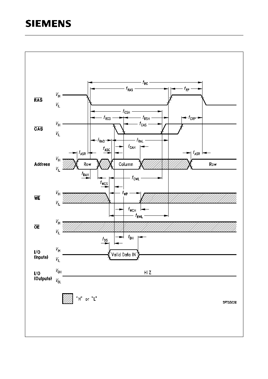
Read Cycle
Semiconductor Group
12
HYB 514405BJ/BLJ-50/-60/-70
1M x 4 EDO - DRAM
Write Cycle (Early Write)
Semiconductor Group
13
HYB 514405BJ/BJL-50/-60/-70
1M x 4 EDO - DRAM
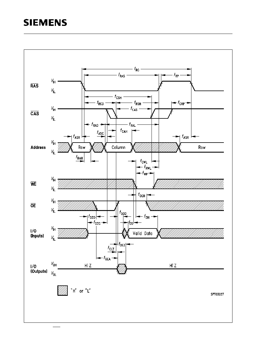
Write Cycle (OE Controlled Write)

Semiconductor Group
14
HYB 514405BJ/BLJ-50/-60/-70
1M x 4 EDO - DRAM
Read-Write (Read-Modify-Write) Cycle

Semiconductor Group
15
HYB 514405BJ/BJL-50/-60/-70
1M x 4 EDO - DRAM
Hyper Page Mode (EDO) Read Cycle

Semiconductor Group
16
HYB 514405BJ/BLJ-50/-60/-70
1M x 4 EDO - DRAM
Hyper Page Mode (EDO) Early Write Cycle

Semiconductor Group
17
HYB 514405BJ/BJL-50/-60/-70
1M x 4 EDO - DRAM
Hyper Page Mode (EDO) Late Write Cycle

Semiconductor Group
18
HYB 514405BJ/BLJ-50/-60/-70
1M x 4 EDO - DRAM
Hyper Page Mode (EDO) Read-Modify-Write Cycle

Semiconductor Group
19
HYB 514405BJ/BJL-50/-60/-70
1M x 4 EDO - DRAM
RAS-Only Refresh Cycle

Semiconductor Group
20
HYB 514405BJ/BLJ-50/-60/-70
1M x 4 EDO - DRAM
CAS-Before-RAS Refresh Cycle

Semiconductor Group
21
HYB 514405BJ/BJL-50/-60/-70
1M x 4 EDO - DRAM
Hidden Refresh Cycle (Read)

Semiconductor Group
22
HYB 514405BJ/BLJ-50/-60/-70
1M x 4 EDO - DRAM
Hidden Refresh Cycle (Early Write)

Semiconductor Group
23
HYB 514405BJ/BJL-50/-60/-70
1M x 4 EDO - DRAM
CAS-Before-RAS Refresh Counter Test Cycle

Semiconductor Group
24
HYB 514405BJ/BLJ-50/-60/-70
1M x 4 EDO - DRAM
Test Mode Entry

Semiconductor Group
25
HYB 514405BJ/BJL-50/-60/-70
1M x 4 EDO - DRAM
Test Mode
As the HYB 514405BJ/BT is organized internally as 512K x 8-bits, a test mode cycle using 8:1
compression can be used to improve test time. Note that in the 1M x 4 version the test time is
reduced by 1/2 for a linear test pattern.
In a test mode "write" the data from each I/O1 pin is written into eight bits simultaneously (all "1" s
or all "0" s).The I/O2-I/O4 inputs are not used for writing in test mode. In test mode "read" each I/O
output is used for indicating the test mode result. If the internal eight bits are equal, the I/O would
indicate a "1". If they were not equal, the I/O would indicate a "0".Note that in test mode ,,read" I/O1-
I/O3 are always driven to ,,ones" ,i.e. all outputs will be ,,1"s for a test mode ,,pass". The WCBR cycle
(WE, CAS before RAS) puts the device into test mode. To exit from test mode, a "CAS before RAS
refresh", "RAS only refresh" or "Hidden refresh" can be used.
Addresses A10R, A10C and A0C are don`t care during test mode.
Package Outlines
P-SOJ-26/20-5
(Small Outline J-Leaded Package)
GPJ05627
Sorts of Packing
Package outlines for tubes, trays etc. are contained in our
Data Book "Package Information".
Dimensions in mm
SMD = Surface Mounted Device