
Semiconductor Group
1
4M
◊
36-Bit EDO-DRAM Module
HYM 364035S/GS-60
Advanced Information
∑
4 194 304 words by 36-Bit organization
∑
Fast access and cycle time
60 ns RAS access time
15 ns CAS access time
104 ns cycle time
∑
Hyper page mode (EDO) capability
25 ns cycle time
∑
Single + 5 V (
±
10 %) supply
∑
Low power dissipation
max. 7260 mW active
CMOS ≠ 66 mW standby
TTL
≠ 132 mW standby
∑
CAS-before-RAS refresh
RAS-only-refresh
Hidden-refresh
∑
12 decoupling capacitors mounted on substrate
∑
All inputs, outputs and clocks fully TTL compatible
∑
72 pin Single in-Line Memory Module (L-SIM-72) with 22.9 mm (900 mil) height
∑
Utilizes 12 4M x 3 DRAM's in 300 mil SOJ packages
∑
2048 refresh cycles / 32 ms
∑
Optimized for use in byte-write parity applications
∑
Tin-Lead contact pads (HYM 364035S-60)
∑
Gold contact pads (HYM 364035GS-60)
4.96
Semiconductor Group
2
HYM 364035S/GS-60
4M
◊
36-Bit EDO-Module
The HYM 364035S/GS-60 is a 16 MByte EDO-DRAM module organized as 4 194 304 words by 36-
Bit in a 72-pin single-in-line package comprising twelve HYB 5117305BJ 4M
◊
3 DRAMs in 300 mil
wide SOJ-packages mounted together with twelve 0.2
µ
F ceramic decoupling capacitors on a PC
board.
The HYB 5117305BJ is described in the data sheet and is fully electrical tested and processed
according to SIEMENS standard quality procedure prior to module assembly. After assembly onto
the board, a further set of electrical tests is performed.
The speed of the module can be detected by the use of four presence detect pins.
The common I/O feature on the HYM 364035S-60 dictates the use of early write cycles.
Ordering Information
Type
Ordering Code
Package
Description
HYM 364035S-60
Q67100-Q3016
L-SIM-72-13
DRAM Module
(access time 60 ns)
HYM 364035GS-60
Q67100-Q3017
L-SIM-72-13
DRAM Module
(access time 60 ns)
Semiconductor Group
3
HYM 364035S/GS-60
4M
◊
36-Bit EDO-Module
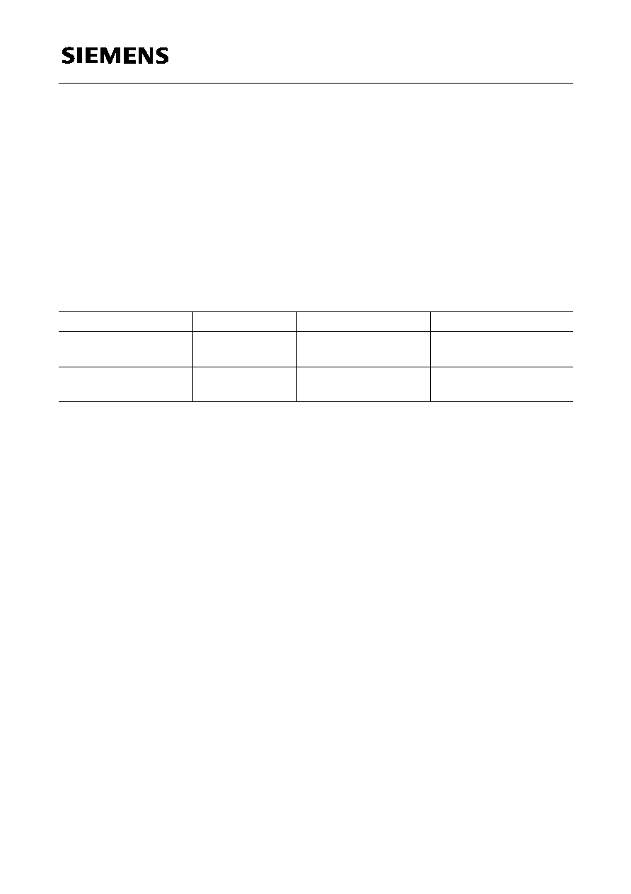
Pin Configuration
(top view)
Pin Names
Presence Detect Pins
A0-A10
Address Inputs for
HYM 364035S/GS
DQ0-DQ35
Data Input/Output
CAS0 - CAS3
Column Address Strobe
RAS0, RAS2
Row Address Strobe
WE
Read/Write Input
V
CC
Power (+ 5 V)
V
SS
Ground
PD
Presence Detect Pin
N.C.
No Connection
-60
PD0
V
SS
PD1
N.C.
PD2
N.C.
PD3
N.C.
Semiconductor Group
4
HYM 364035S/GS-60
4M
◊
36-Bit EDO-Module
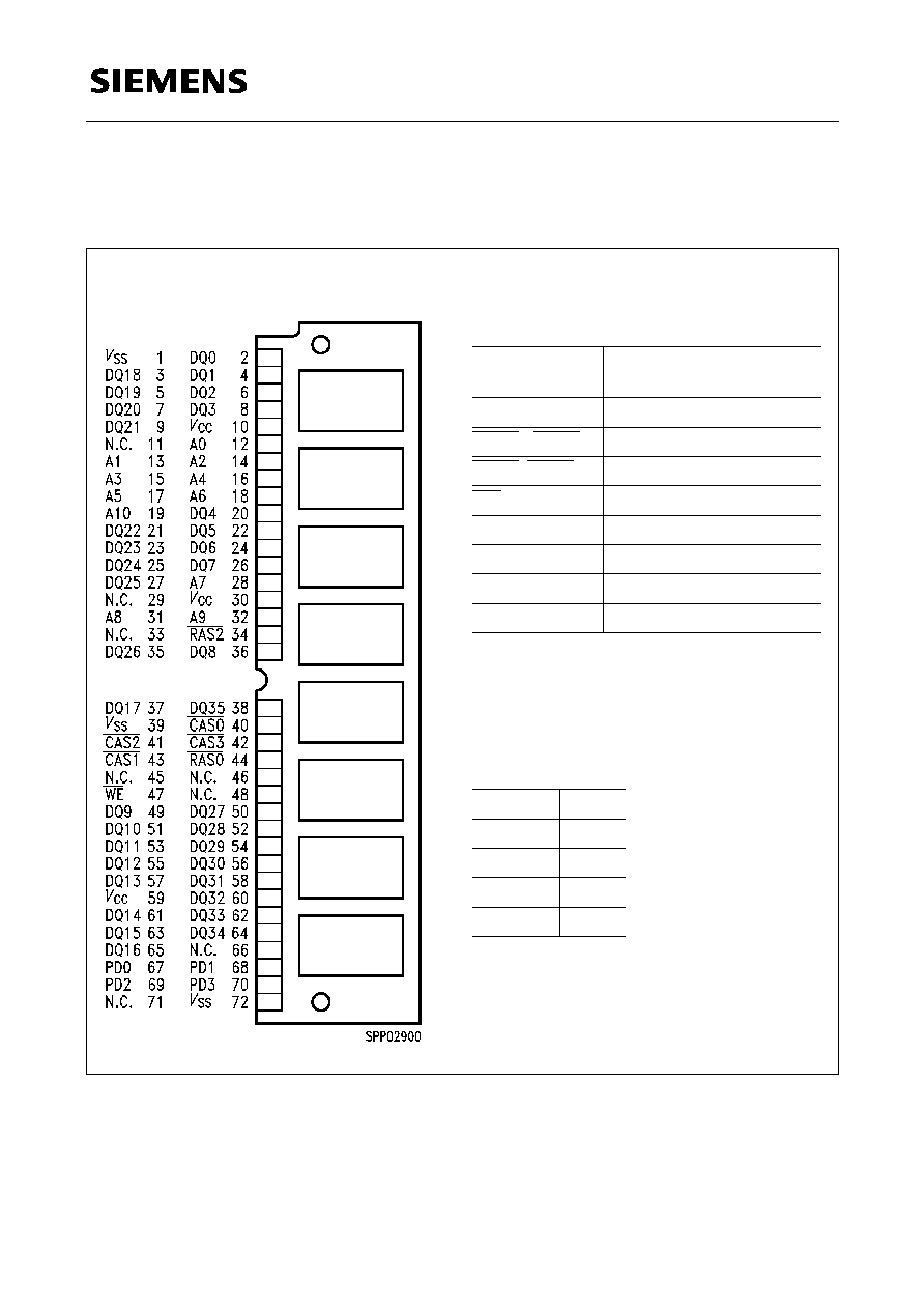
Block Diagram

Semiconductor Group
5
HYM 364035S/GS-60
4M
◊
36-Bit EDO-Module
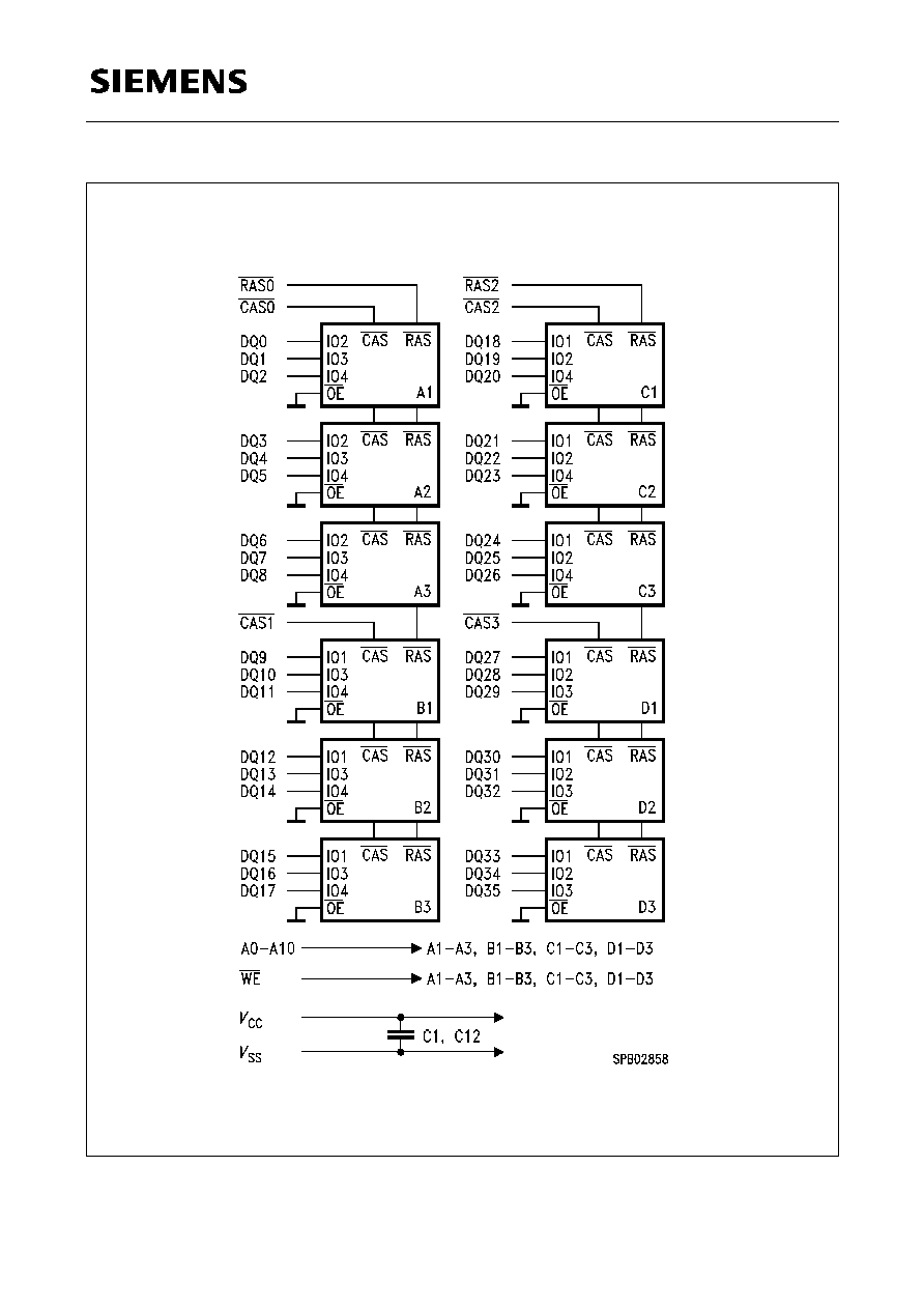
Absolute Maximum Ratings
Operation temperature range ......................................................................................... 0 to + 70 ∞C
Storage temperature range......................................................................................... ≠ 55 to 125 ∞C
Input/output voltage ........................................................................ ≠ 0.5 V to min (
V
CC
+ 0.5, 7.0) V
Power supply voltage...................................................................................................... ≠ 1 to + 7 V
Power dissipation................................................................................................................... 9.24 W
Data out current (short circuit) ................................................................................................ 50 mA
Note:
Stresses above those listed under "Absolute Maximum Ratings" may cause permanent
damage of the device. Exposure to absolute maximum rating conditions for extended periods
may affect device reliability.
DC Characteristics
T
A
= 0 to 70 ∞C,
V
CC
= 5 V
±
10 %
Parameter
Symbol
Limit Values
Unit
Test
Condition
min.
max.
Input high voltage
V
IH
2.4
V
CC
+ 0.5
V
1)
Input low voltage
V
IL
≠ 0.5
0.8
V
1)
Output high voltage (
I
OUT
= ≠ 5 mA)
V
OH
2.4
≠
V
1)
Output low voltage (
I
OUT
= 4.2 mA)
V
OL
≠
0.4
V
1)
Input leakage current
(0 V <
V
IN
< 6.5 V, all other pins = 0 V)
I
I(L)
≠ 80
80
µ
A
1)
Output leakage current
(DO is disabled, 0 V <
V
OUT
< 5.5 V)
I
O(L)
≠ 10
10
µ
A
1)
Average
V
CC
supply current
(RAS, CAS, address cycling,
t
RC
=
t
RC
min)
-60 ns version
I
CC1
≠
1320
mA
2),3),4)
Standby
V
CC
supply current
(RAS = CAS =
V
IH
)
I
CC2
≠
24
mA
Average
V
CC
supply current
during RAS only refresh cycles
(RAS cycling, CAS =
V
IH
,
t
RC
=
t
RC
min)
-60 ns version
I
CC3
≠
1320
mA
2),4)
Semiconductor Group
6
HYM 364035S/GS-60
4M
◊
36-Bit EDO-Module
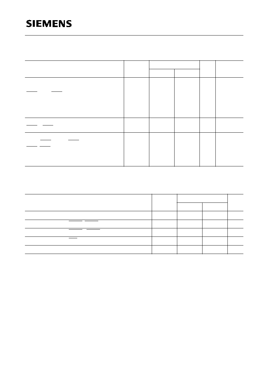
DC Characteristics
1)
(cont'd)
Capacitance
T
A
= 0 to 70 ∞C,
V
CC
= 5 V
±
10 %,
f
= 1 MHz
Parameter
Symbol
Limit Values
Unit
Test
Condition
min.
max.
Average
V
CC
supply current
during hyper page mode (EDO)
(RAS =
V
IL
, CAS, address cycling,
t
PC
=
t
PC
min)
-60 ns version
I
CC4
≠
660
mA
2),3),4)
Standby
V
CC
supply current
(RAS = CAS =
V
CC
≠ 0.2 V)
I
CC5
≠
12
mA
1)
Average
V
CC
supply current
during CAS-before-RAS refresh mode
(RAS, CAS cycling,
t
RC
=
t
RC
min)
-60 ns version
I
CC6
≠
1320
mA
2),4)
Parameter
Symbol
Limit Values
Unit
min.
max.
Input capacitance (A0 to A10)
C
I1
≠
90
pF
Input capacitance (RAS0, RAS2)
C
I2
≠
45
pF
Input capacitance (CAS0 - CAS3)
C
I3
≠
40
pF
Input capacitance (WE)
C
I4
≠
90
pF
I/O capacitance(DQ0-DQ35)
C
IO1
≠
20
pF

Semiconductor Group
7
HYM 364035S/GS-60
4M
◊
36-Bit EDO-Module
AC Characteristics
5)6)
T
A
= 0 to 70 ∞C,
V
CC
= 5 V
±
10 %,
t
T
= 2 ns
Parameter
Symbol
Unit
Note
-60
min.
max.
Common Parameters
Random read or write cycle time
t
RC
104
≠
ns
RAS precharge time
t
RP
40
≠
ns
RAS pulse width
t
RAS
60
10k
ns
CAS pulse width
t
CAS
10
10k
ns
Row address setup time
t
ASR
0
≠
ns
Row address hold time
t
RAH
10
≠
ns
Column address setup time
t
ASC
0
≠
ns
Column address hold time
t
CAH
10
≠
ns
RAS to CAS delay time
t
RCD
14
45
ns
RAS to column address delay time
t
RAD
12
30
ns
RAS hold time
t
RSH
15
≠
ns
CAS hold time
t
CSH
60
≠
ns
CAS to RAS precharge time
t
CRP
5
≠
ns
Transition time (rise and fall)
t
T
1
50
ns
7
Refresh period
t
REF
≠
32
ms
Read Cycle
Access time from RAS
t
RAC
≠
60
ns
8, 9
Access time from CAS
t
CAC
≠
15
ns
8, 9
Access time from column address
t
AA
≠
30
ns
8,10
Column address to RAS lead time
t
RAL
30
≠
ns
Read command setup time
t
RCS
0
≠
ns
Read command hold time
t
RCH
0
≠
ns
11
Read command hold time referenced to RAS
t
RRH
0
≠
ns
11
CAS to output in low-Z
t
CLZ
0
≠
ns
8
Output buffer turn-off delay
t
OFF
0
15
ns
12

Semiconductor Group
8
HYM 364035S/GS-60
4M
◊
36-Bit EDO-Module
Early Write Cycle
Write command hold time
t
WCH
10
≠
ns
Write command pulse width
t
WP
10
≠
ns
Write command setup time
t
WCS
0
≠
ns
13
Write command to RAS lead time
t
RWL
15
≠
ns
Write command to CAS lead time
t
CWL
15
≠
ns
Data setup time
t
DS
0
≠
ns
14
Data hold time
t
DH
10
≠
ns
14
Hyper Page Mode (EDO) Cycle
Hyper page mode (EDO) cycle time
t
HPC
25
≠
ns
CAS precharge time
t
CP
10
≠
ns
Access time from CAS precharge
t
CPA
≠
32
ns
7
Output data hold time
t
COH
5
≠
ns
RAS pulse width in hyper page mode
t
RAS
60
200k
ns
CAS precharge to RAS Delay
t
RHCP
32
≠
ns
CAS before RAS Refresh Cycle
CAS setup time
t
CSR
10
≠
ns
CAS hold time
t
CHR
10
≠
ns
RAS to CAS precharge time
t
RPC
5
≠
ns
Write to RAS precharge time
t
WRP
10
≠
ns
Write hold time referenced to RAS
t
WRH
10
≠
ns
AC Characteristics (cont'd)
5)6)
T
A
= 0 to 70 ∞C,
V
CC
= 5 V
±
10 %,
t
T
= 2 ns
Parameter
Symbol
Unit
Note
-60
min.
max.

Semiconductor Group
9
HYM 364035S/GS-60
4M
◊
36-Bit EDO-Module
Notes:
1) All voltages are referenced to
V
SS
.
2)
I
CC1
,
I
CC3
,
I
CC4
and
I
CC6
depend on cycle rate.
3)
I
CC1
and
I
CC4
depend on output loading. Specified values are obtained with the output open.
4) Address can be changed once or less while RAS =
V
IL
. In case of
I
CC4
it can be changed once or less during
a hyper page mode (EDO) cycle.
5) An initial pause of 200
µ
s is required after power-up followed by 8 RAS cycles of which at least one cycle has
to be a refresh cycle, before proper device operation is achieved. In case of using the internal refresh counter,
a minimum of 8 CAS-before-RAS initialization cycles instead of 8 RAS cycles are required.
6) AC measurements assume
t
T
= 2 ns.
7)
V
IH
(min.)
and
V
IL (max.)
are reference levels for measuring timing of input signals. Transition times are also
measured between
V
IH
and
V
IL
.
8) Measured with the specified current load and 100 pF at
V
OL
= 0.8 V and
V
OH
= 2.0 V. Access time is determined
by the latter of
t
RAC
,
t
CAC
,
t
AA
,
t
CPA
.
t
CAC
is measured from tristate.
9) Operation within the
t
RCD (max.)
limit ensures that
t
RAC (max.)
can be met.
t
RCD (max.)
is specified as a reference point
only. If
t
RCD
is greater than the specified
t
RCD (max.)
limit, then access time is controlled by
t
CAC
.
10) Operation within the
t
RAD (max.
)
limit ensures that
t
RAC (max.)
can be met.
t
RAD (max.)
is specified as a reference point
only. If
t
RAD
is greater than the specified
t
RAD (max.)
limit, then access time is controlled by
t
AA
.
11) Either
t
RCH
or
t
RRH
must be satisfied for a read cycle.
12)
t
OFF (max.)
define the time at which the output achieves the open-circuit conditions and are not referenced to
output voltage levels.
t
OFF
is referenced from the rising edge of RAS or CAS, whichever occurs last.
13)
t
WCS
is not a restrictive operating parameter. This is included in the data sheet as electrical characteristics only.
If
t
WCS
>
t
WCS (min.)
, the cycle is an early write cycle and data out pin will remain open-circuit (high impedance)
through the entire cycle.
14) These parameters are referenced to the CAS leading edge.
Semiconductor Group
10
HYM 364035S/GS-60
4M
◊
36-Bit EDO-Module
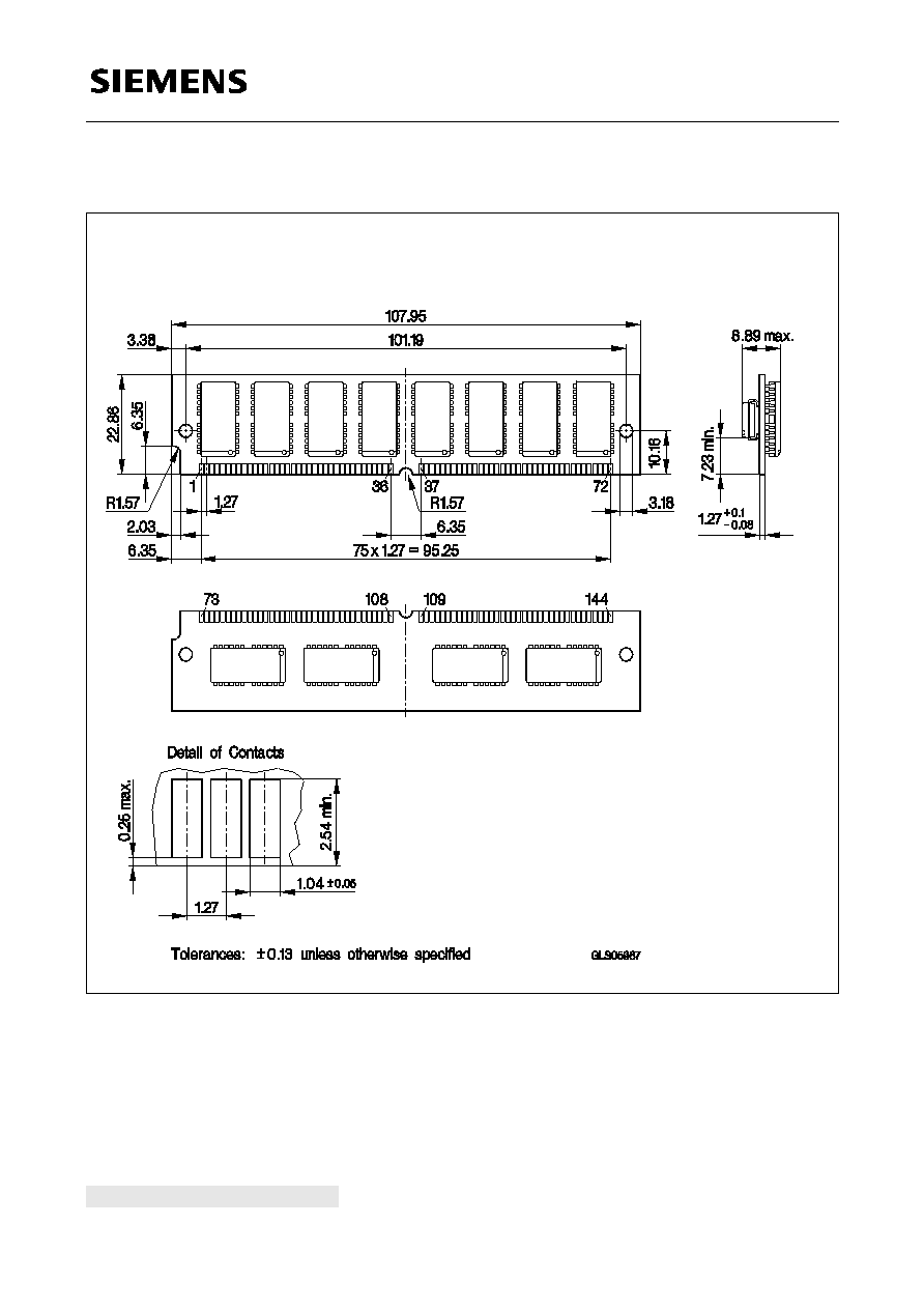
Package Outline
L-SIM-72-13
(Single In-line Module)
Sorts of Packing
Package outlines for tubes, trays etc. are contained in our
Data Book "Package Information".
Dimensions in mm
SMD = Surface Mounted Device