Semiconductor Group
125
01.95
512kx8-Bit Dynamic RAM
Advanced Information
∑
512 288 words by 8-bit organization
∑
0 to 70 ∞C operating temperature
∑
Fast access and cycle time
RAS access time:
60 ns (-60 version)
70 ns (-70 version)
80 ns (-80 version)
CAS access time:
20 ns
Cycle time:
110 ns (-60 version)
130 ns (-70 version)
150 ns (-80 version)
∑
Fast page mode cycle time
45 ns (-60 version)
45 ns (-70 version)
50 ns (-80 version)
∑
Single + 5 V (
±
10 %) supply with a
built-in
V
bb
generator
Ordering Information
Type
Ordering Code
Package
Descriptions
HYB 514800BJ-60
Q67100-Q849
P-SOJ-28-2
DRAM
(access time 60 ns)
HYB 514800BJ-70
Q67100-Q850
P-SOJ-28-2
DRAM
(access time 70 ns)
HYB 514800BJ-80
Q67100-Q851
P-SOJ-28-2
DRAM
(access time 80 ns)
HYB 514800BJ -60/-70/-80
∑
Low power dissipation
max. 605 mW active (-60 version)
max. 550 mW active (-70 version)
max. 468 mW active (-80 version)
∑
Standby power dissipation:
11 mW standby standby (TTL)
5.5 mW max.standby (CMOS)
∑
Output unlatched at cycle end allows two-
dimensional chip selection
∑
Read, write, read-modify write, CAS-before-
RAS refresh, RAS-only refresh, hidden
refresh, fast page mode capability
∑
All inputs and outputs TTL-compatible
∑
1024 refresh cycles / 16 ms
∑
Plastic Packages: P-SOJ-28-2 400 mil width

Semiconductor Group
126
The HYB 514800BJ is the new generation dynamic RAM organized as 512 288 words by 8-bit. The
HYB 514800BJ utilizes CMOS silicon gate process as well as advances circuit techniques to
provide wide operation margins, both internally and for the system user. Multiplexed address inputs
permit the HYB 514800BJ to be packed in a standard plastic 400mil wide P-SOPJ-28 package. This
package size provides high system bit densities and is compatible with commonly used automatic
testing and insertion equipment. System oriented feature include single + 5 V (
±
10 %) power
supply, direct interfacing with high performance logic device families such as Schottky TTL.
Pin Definitions and Functions
Pin Configuration
(top view)
A0-A8,A9R
Address Input
RAS
Row Address Strobe
CAS
Column Address Strobe
WRITE
Read/Write Input
OE
Output Enable
I
O1 -
I
O8
Data Input/Output
N.C.
No Connection
V
CC
Power Supply (+ 5 V)
V
SS
Ground (0 V)
P-SOJ-28-2 ( 400 mil width)
HYB 514800BJ -60/-70/-80
512k x 8 DRAM
Semiconductor Group
127
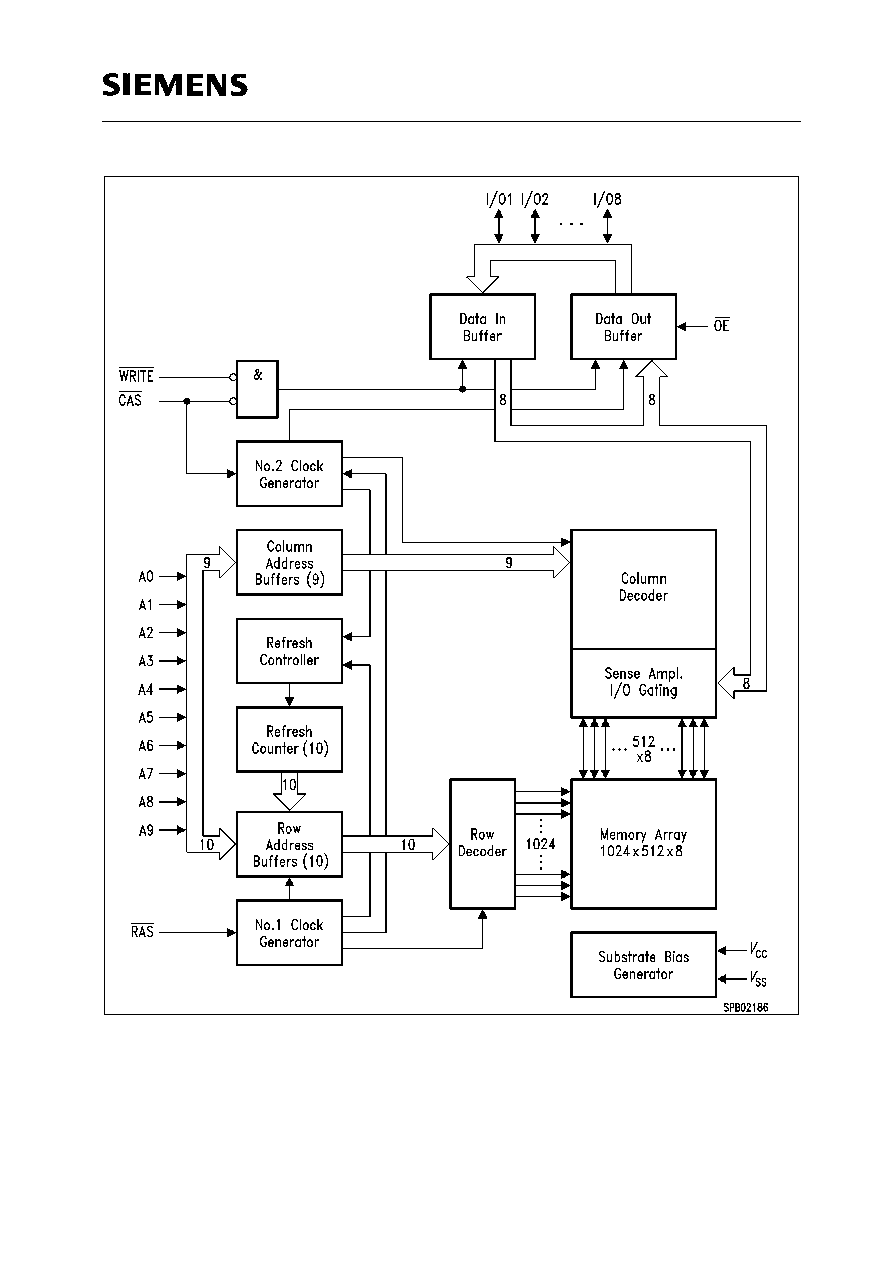
Block Diagram
HYB 514800BJ -60/-70/-80
512k x 8 DRAM
Semiconductor Group
128
Absolute Maximum Ratings
Operating temperature range ............................................................................................0 to 70 ∞C
Storage temperature range......................................................................................≠ 55 to + 150 ∞C
Soldering temperature ............................................................................................................260 ∞C
Soldering time .............................................................................................................................10 s
Input/output voltage ........................................................................................................ ≠ 1 to + 7 V
Power Supply voltage ..................................................................................................... ≠ 1 to + 7 V
Data out current (short circuit) ................................................................................................ 50 mA
Note:
Stresses above those listed under "Absolute Maximum Ratings" may cause permanent
damage of the device. Exposure to absolute maximum rating conditions for extended periods
may affect device reliability.
DC Characteristics
T
A
= 0 to 70 ∞C,
V
SS
= 0 V,
V
CC
= 5 V
±
10 %,
t
T
= 5 ns
Parameter
Symbol
Limit Values
Unit Test
Condition
min.
max.
Input high voltage
V
ih
2.4
6.5
V
1)
Input low voltage
V
il
≠ 1.0
0.8
V
1)
Output high voltage (
I
OUT
= ≠ 5 mA)
V
oh
2.4
≠
V
1)
Output low voltage (
I
OUT
= 4.2 mA)
V
ol
≠
0.4
V
1)
Input leakage current, any input
(0 V <
V
in
< 7, all other input = 0 V)
I
I
(L)
≠ 10
10
µ
A
1)
Output leakage current
(DO is disabled, 0 <
V
OUT
<
V
CC
)
I
o(L)
≠ 10
10
µ
A
1)
Average
V
CC
supply current
-60 version
-70 version
-80 version
I
CC1
≠
≠
≠
110
100
90
mA
2) 3)
Standby
V
CC
supply current
(RAS = CAS =
V
ih
)
I
CC2
≠
2
mA
≠
Average
V
CC
supply current during RAS-only
refresh cycles
-60 version
-70 version
-80 version
I
CC3
≠
≠
≠
110
100
90
mA
2)
Average
V
CC
supply current during fast page
mode operation
-60 version
-70 version
-80 version
I
CC4
≠
≠
≠
70
60
50
mA
2) 3)
HYB 514800BJ -60/-70/-80
512k x 8 DRAM

Semiconductor Group
129
Standby
V
CC
supply current
(RAS = CAS =
V
CC
≠ 0.2 V)
I
CC5
≠
1
mA
1)
Average
V
CC
supply current during
CAS before RAS refresh mode
-60 version
-70 version
-80 version
I
CC6
≠
≠
≠
110
100
90
mA
2)
DC Characteristics (cont'd)
T
A
= 0 to 70 ∞C,
V
SS
= 0 V,
V
CC
= 5 V
±
10 %,
t
T
= 5 ns
Parameter
Symbol
Limit Values
Unit Test
Condition
min.
max.
HYB 514800BJ -60/-70/-80
512k x 8 DRAM