Semiconductor Group
591
1M
◊
36-Bit Dynamic RAM Module
(2M
◊
18-Bit Dynamic RAM Module)
Advanced Information
HYM 361120/40S/GS-60/-70
∑
1 048 576 words by 36-bit organization
(alternative 2 097 152 words by 18-bit)
∑
Fast access and cycle time
60 ns access time
110 ns cycle time (-60 version)
70 ns access time
130 ns cycle time (-70 version)
∑
Fast page mode capability with
40 ns cycle time (-60 version)
45 ns cycle time (-70 version)
∑
Single + 5 V (
±
10 %) supply
∑
Low power dissipation
max. 6820 mW active (-60 version)
max. 6160 mW active (-70 version)
CMOS ≠ 66 mW standby
TTL
≠ 132 mW standby
∑
CAS-before-RAS refresh, RAS-only-refresh,
Hidden refresh
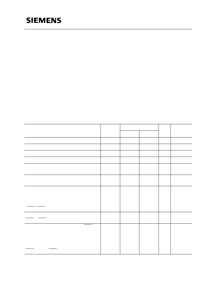
Ordering Information
Type
Ordering Code
Package
Descriptions
HYM 361140S-60
Q67100-Q959
L-SIM-72-8
DRAM module (access time 60 ns)
HYM 361140S-70
Q67100-Q958
L-SIM-72-8
DRAM module (access time 70 ns)
HYM 361120S-60
Q67100-Q942
L-SIM-72-3
DRAM module (access time 60 ns)
HYM 361120S-70
Q67100-Q741
L-SIM-72-3
DRAM module (access time 70 ns)
HYM 361140GS-60
Q67100-Q1019
L-SIM-72-8
DRAM module (access time 60 ns)
HYM 361140GS-70
Q67100-Q651
L-SIM-72-8
DRAM module (access time 70 ns)
HYM 361120GS-60
Q67100-Q961
L-SIM-72-3
DRAM module (access time 60 ns)
HYM 361120GS-70
Q67100-Q960
L-SIM-72-3
DRAM module (access time 70 ns)
Semiconductor Group
591
06.94
∑
12 decoupling capacitors mounted on
substrate
∑
All inputs, outputs and clock fully TTL
compatible
∑
72 pin Single in-Line Memory Module
∑
Utilizes four 1M
◊
1-DRAMs and eight
1M
◊
4-DRAMs in 300 mil SOJ packages
∑
1024 refresh cycles/16 ms
∑
Tin-Lead contact pads (S - version)
∑
Gold contact pads (GS - version)
∑
HYM 321140S: single sided module with
31.75 mm (1250 mil) height
∑
HYM 321120S: double sided module with
25.40 mm (1000 mil) height
Semiconductor Group
592
The HYM 361120/40S/GS-60/-70 is a 4 MByte DRAM module organized as 1 048 576 words by
36-bit in a 72-pin single-in-line package comprising four HYB 511000BJ 1M
◊
1 DRAMs and eight
HYB 514400BJ 1M
◊
4 DRAMs in 300 mil wide SOJ-packages mounted together with twelve
0.2
µ
F ceramic decoupling capacitors on a PC board.
The HYM 361120/40S/GS-60/-70 can also be used as a 2 097 152 words by 18-bits dynamic RAM
module by means of connecting DQ0 and DQ18, DQ1 and DQ19, DQ2 and DQ20, ..., DQ17 and
DQ35, respectively.
Each HYB 511000BJ and HYB 514400BJ is described in the data sheet and is fully electrically
tested and processed according to Siemens standard quality procedure prior to module assembly.
After assembly onto the board, a further set of electrical tests is performed.
The speed of the module can be detected by the use of four presence detect pins.
The common I/O feature on the HYM 361120/40S/GS-60/-70 dictates the use of early write cycles.
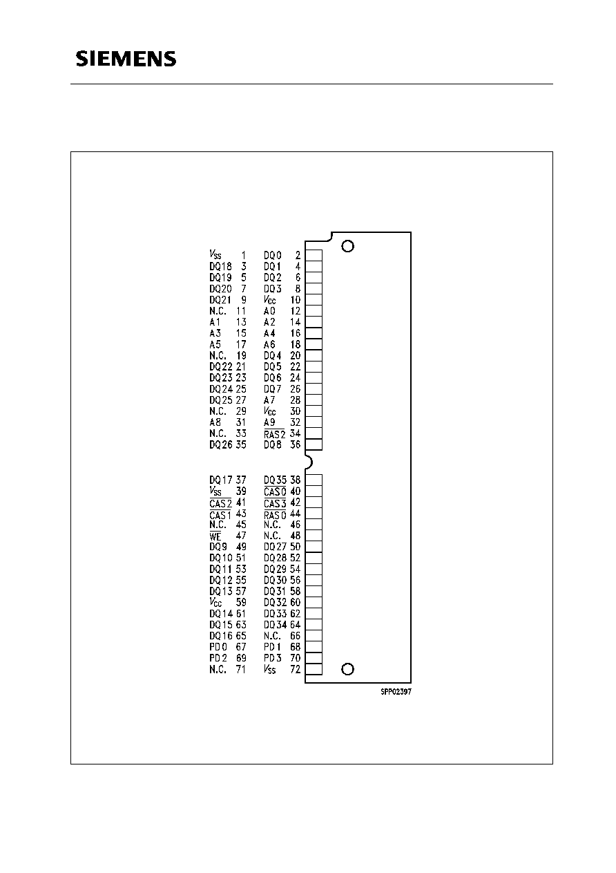
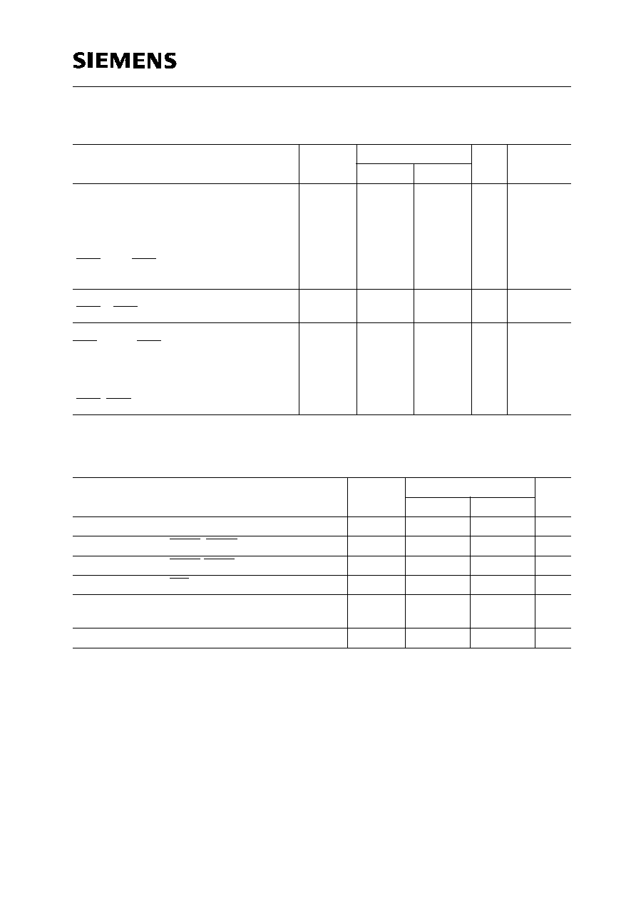
Pin Definitions and Functions
Presence Detect Pins
Pin No.
Function
A0-A9
Address Inputs
DQ0-DQ35
Data Input/Output
CAS0 - CAS3
Column Address Strobe
RAS0, RAS2
Row Address Strobe
WE
Read/Write Input
V
CC
Power (+ 5 V)
V
SS
Ground
PD
Presence Detect Pin
N.C.
No Connection
-60
-70
PD0
V
SS
V
SS
PD1
V
SS
V
SS
PD2
N.C.
V
SS
PD3
N.C.
N.C.
HYM 361120/40S/GS-60/-70
1M
◊
36-Bit
Semiconductor Group
593
HYM 361120/40S/GS-60/-70
1M
◊
36-Bit
Pin Configuration
(top view)
Semiconductor Group
594
HYM 361120/40S/GS-60/-70
1M
◊
36-Bit
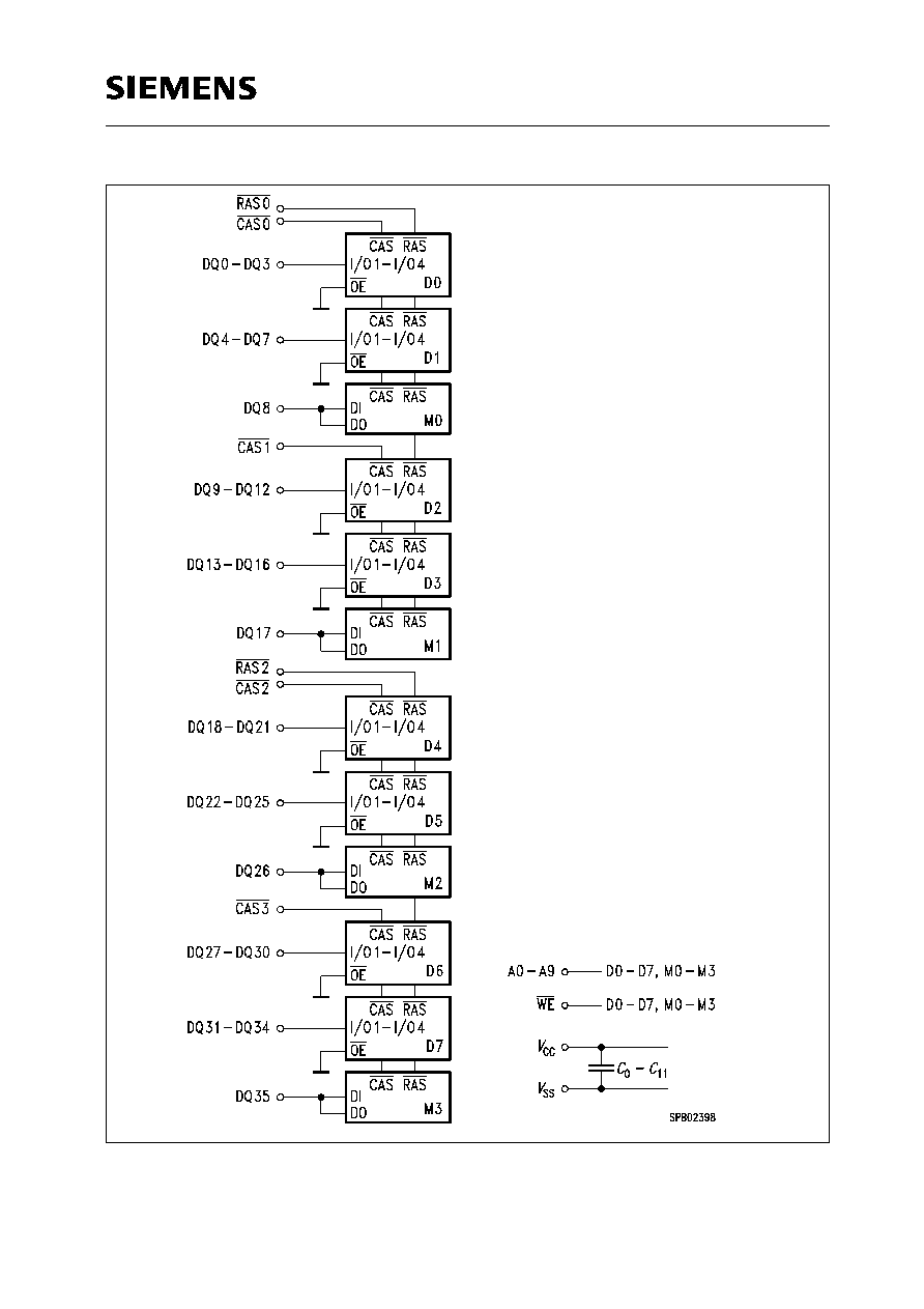
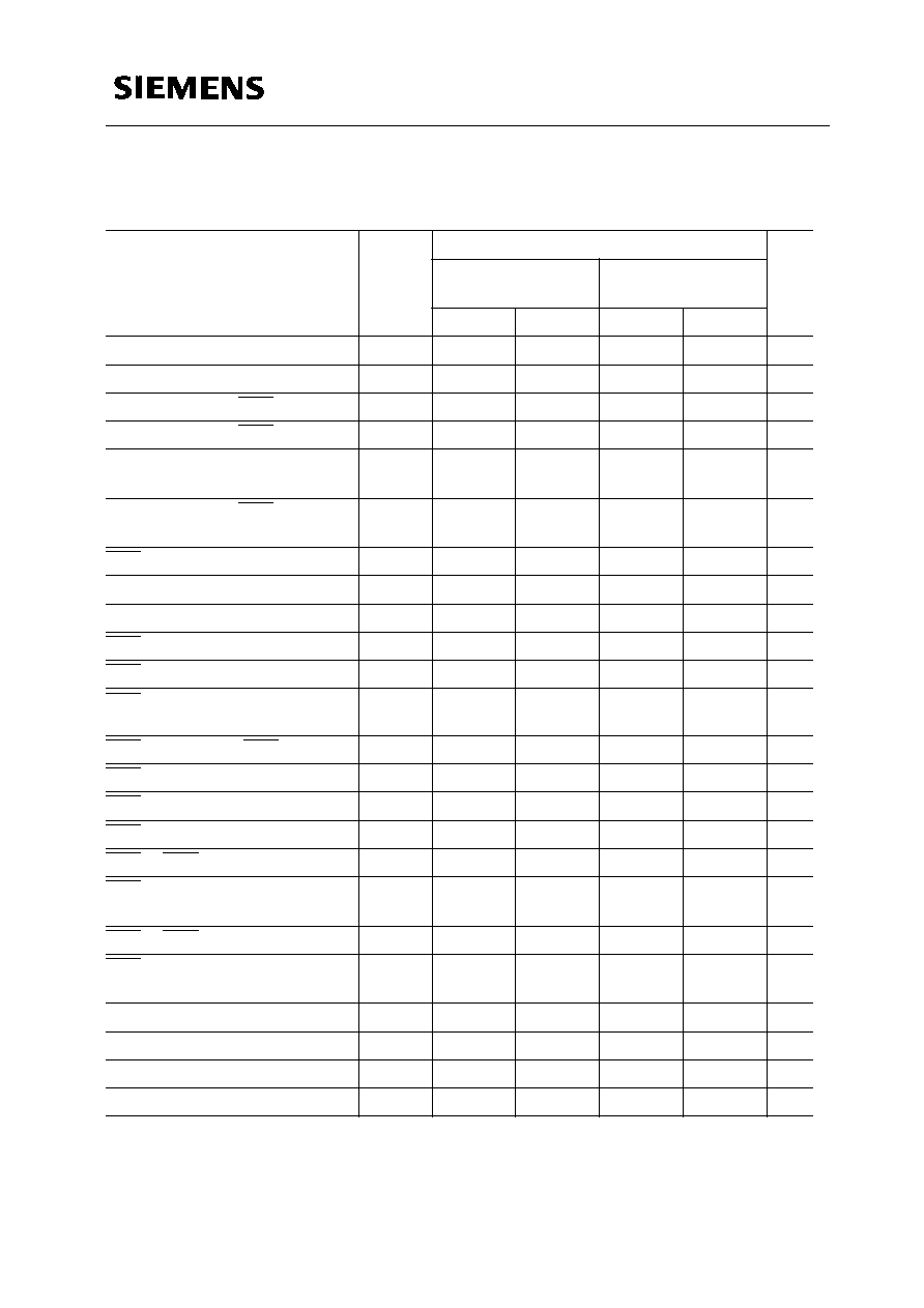
Block Diagram
Semiconductor Group
595
Absolute Maximum Ratings
Operating temperature range ......................................................................................... 0 to + 70 ∞C
Storage temperature range...................................................................................... ≠ 55 to + 125 ∞C
Soldering temperature ............................................................................................................ 260 ∞C
Soldering time ............................................................................................................................. 10 s
Input/output voltage ........................................................................................................ ≠ 1 to + 7 V
Power supply voltage...................................................................................................... ≠ 1 to + 7 V
Power dissipation................................................................................................................... 8.68 W
Data out current (short circuit) ................................................................................................ 50 mA
Note: Stresses above those listed under "Absolute Maximum Ratings" may cause permanent
damage to the device. Exposure to absolute maximum rating conditions for extended periods
may affect device reliability.
DC Characteristics
1)
T
A
= 0 to 70 ∞C;
V
CC
= 5 V
±
10 %
Parameter
Symbol
Limit Values
Unit
Test
Condition
min.
max.
Input high voltage
V
IH
2.4
5.5
V
≠
Input low voltage
V
IL
≠ 1.0
0.8
V
≠
Output high voltage (
I
OUT
= ≠ 5 mA)
V
OH
2.4
≠
V
≠
Output low voltage (
I
OUT
= 4.2 mA)
V
OL
≠
0.4
V
≠
Input leakage current
(0 V <
V
IN
< 6.5 V, all other pins = 0 V)
I
I(L)
≠ 20
20
µ
A
≠
Output leakage current
(DO is disabled, 0 V <
V
OUT
< 5.5 V)
I
O(L)
≠ 10
10
µ
A
≠
Average
V
CC
supply current:
-60 version
-70 version
(RAS, CAS, address cycling,
t
RC
=
t
RC
min.)
I
CC1
≠
≠
1240
1120
mA
mA
2), 3)
Standby
V
CC
supply current
(RAS = CAS =
V
IH
)
I
CC2
≠
24
mA
≠
Average
V
CC
supply current during RAS
only refresh cycles:
-60 version
-70 version
(RAS cycling, CAS =
V
IH
, t
RC
=
t
RC
min.)
I
CC3
≠
≠
1240
1120
mA
mA
2)
HYM 361120/40S/GS-60/-70
1M
◊
36-Bit
Semiconductor Group
596
HYM 361120/40S/GS-60/-70
1M
◊
36-Bit
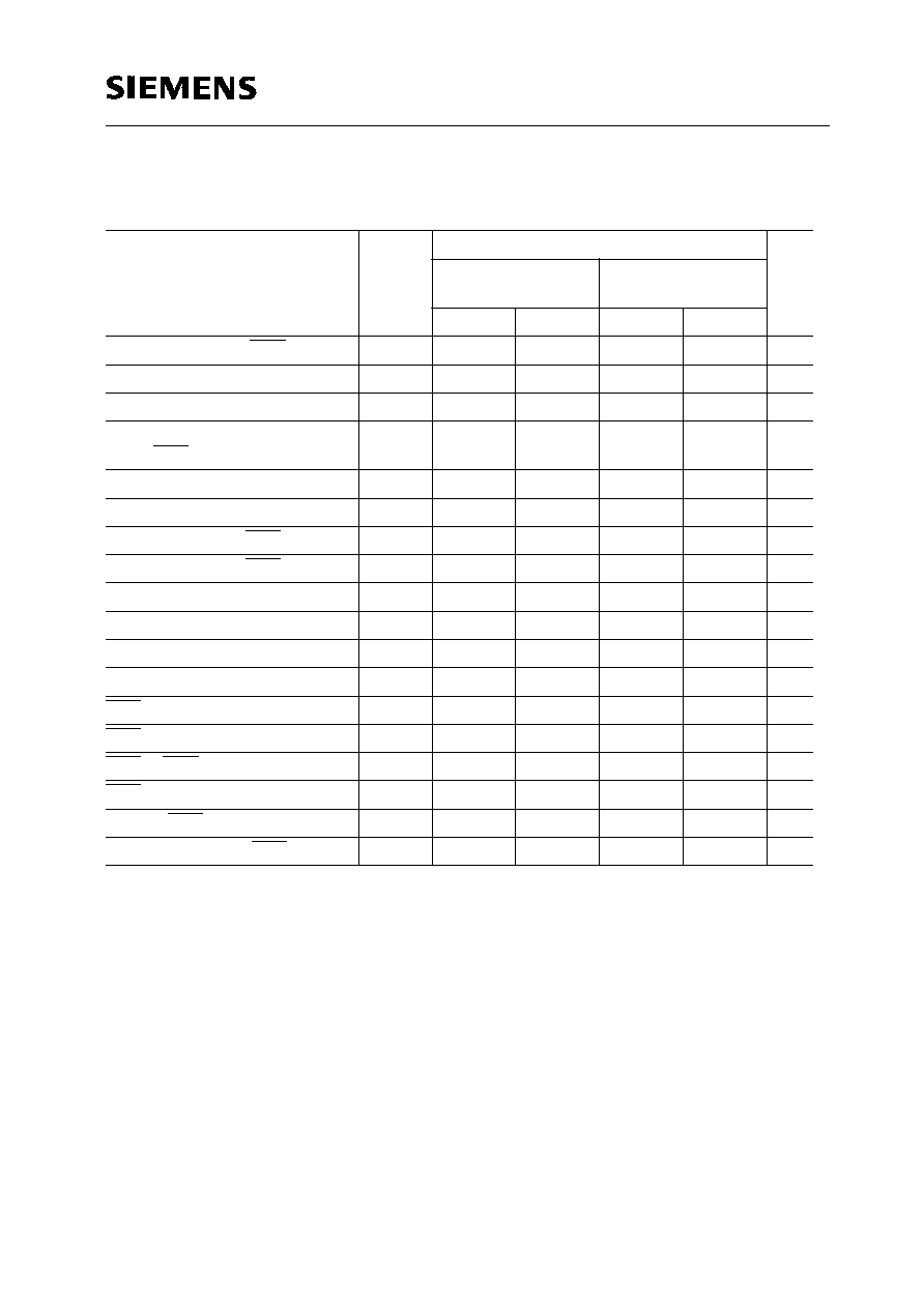
DC Characteristics (cont'd)
1)
Capacitance
T
A
= 0 to 70 ∞C;
V
CC
= 5 V
±
10 %;
f
= 1 MHz
Parameter
Symbol
Limit Values
Unit
Test
Condition
min.
max.
Average
V
CC
supply current during fast
page mode:
-60 version
-70 version
(RAS =
V
IL,
CAS, address cycling
t
PC
=
t
PC
min.)
I
CC4
≠
≠
840
720
mA
mA
2), 3)
Standby
V
CC
supply current
(RAS = CAS =
V
CC
≠ 0.2 V)
I
CC5
≠
12
mA
≠
Average
V
CC
supply current during
CAS-before-RAS refresh mode:
-60 version
-70 version
(RAS, CAS cycling
, t
RC
=
t
RC
min.)
I
CC6
≠
≠
1240
1120
mA
mA
1)
Parameter
Symbol
Limit Values
Unit
min.
max.
Input capacitance (A0 to A9)
C
I1
≠
80
pF
Input capacitance (RAS0, RAS2)
C
I2
≠
42
pF
Input capacitance (CAS0-CAS3)
C
I3
≠
35
pF
Input capacitance (WE)
C
I4
≠
80
pF
I/O capacitance (DQ0-DQ7, DQ9-DQ16,
DQ18-DQ25, DQ27-DQ34)
C
IO1
≠
15
pF
I/O capacitance (DQ8, DQ17, DQ26, DQ35)
C
IO2
≠
20
pF
Semiconductor Group
597
AC Characteristics
4) 5)
T
A
= 0 to 70 ∞C;
V
CC
= 5 V
±
10 %;
t
T
= 5 ns
.
Parameter
Symbol
Limit Values
Unit
HYM
361120/40S/GS-60
HYM
361120/40S/GS-70
min.
max.
min.
max.
Random read or write cycle time
t
RC
110
≠
130
≠
ns
Fast page mode cycle time
t
PC
40
≠
45
≠
ns
Access time from RAS
6) 11) 12)
t
RAC
≠
60
≠
70
ns
Access time from CAS
6) 11)
t
CAC
≠
15
≠
20
ns
Access time from column
address
6) 12)
t
AA
≠
30
≠
35
ns
Access time from CAS
prech arge
6)
t
CPA
≠
35
≠
40
ns
CAS to output in low-Z
6)
t
CLZ
0
≠
0
≠
ns
Output buffer turn-off delay
7)
t
OFF
0
20
0
20
ns
Transition time (rise and fall)
5)
t
T
3
50
3
50
ns
RAS precharge time
t
RP
40
≠
50
≠
ns
RAS pulse width
t
RAS
60
10000
70
10000
ns
RAS pulse width
(fast page mode)
t
RASP
60
200000
70
200000
ns
CAS precharge to RAS delay
t
RHCP
35
≠
40
≠
ns
RAS hold time
t
RSH
15
≠
20
≠
ns
CAS hold time
t
CSH
60
≠
70
≠
ns
CAS pulse width
t
CAS
15
10000
20
10000
ns
RAS to CAS delay time
11)
t
RCD
20
45
20
50
ns
RAS to column address
delay time
12)
t
RAD
15
30
15
35
ns
CAS to RAS precharge time
t
CRP
5
≠
5
≠
ns
CAS precharge time
(fast page mode)
t
CP
10
≠
10
≠
ns
Row address setup time
t
ASR
0
≠
0
≠
ns
Row address hold time
t
RAH
10
≠
10
≠
ns
Column address setup time
t
ASC
0
≠
0
≠
ns
Column address hold time
t
CAH
15
≠
15
≠
ns
HYM 361120/40S/GS-60/-70
1M
◊
36-Bit
Semiconductor Group
598
AC Characteristics (cont'd)
4) 5)
T
A
= 0 to 70 ∞C;
V
CC
= 5 V
±
10 %;
t
T
= 5 ns
.
Parameter
Symbol
Limit Values
Unit
HYM
361120/40S/GS-60
HYM
361120/40S/GS-70
min.
max.
min.
max.
Column address to RAS lead time
t
RAL
30
≠
35
≠
ns
Read command setup time
t
RCS
0
≠
0
≠
ns
Read command hold time
8)
t
RCH
0
≠
0
≠
ns
Read command hold time
ref. to RAS
8)
t
RRH
0
≠
0
≠
ns
Write command hold time
t
WCH
10
≠
15
≠
ns
Write command pulse width
t
WP
10
≠
15
≠
ns
Write command to RAS lead time
t
RWL
15
≠
20
≠
ns
Write command to CAS lead time
t
CWL
15
≠
20
≠
ns
Data setup time
9 )
t
DS
0
≠
0
≠
ns
Data hold time
9 )
t
DH
15
≠
15
≠
ns
Refresh period
t
REF
≠
16
≠
16
ms
Write command setup time
10)
t
WCS
0
≠
0
≠
ns
CAS setup time
13)
t
CSR
5
≠
5
≠
ns
CAS hold time
13)
t
CHR
15
≠
15
≠
ns
RAS to CAS precharge time
t
RPC
0
≠
0
≠
ns
CAS precharge time
13)
t
CP
10
≠
10
≠
ns
Write to RAS precharge time
13)
t
WRP
10
≠
10
≠
ns
Write to time ref. to RAS
13)
t
WRH
10
≠
10
≠
ns
HYM 361120/40S/GS-60/-70
1M
◊
36-Bit
Semiconductor Group
599
Notes
1) All voltages are referenced to
V
SS
.
2)
I
CC1
,
I
CC3
,
I
CC4
and
I
CC6
depend on cycle rate.
3)
I
CC1
and
I
CC4
depend on output loading. Specified values are measured with the output open.
4) An initial pause of 200
µ
s is required after power-up followed by 8 RAS cycles out of which at least one cycle
has to be a refresh cycle before proper device operation is achieved. In case of using internal refresh counter,
a minimum of 8 CAS-before-RAS initialization cycles instead of 8 RAS cycles are required.
5)
V
IH
(min.)
and
V
IL
(max.)
are reference levels for measuring timing of input signals. Transition times are also
measured between
V
IH
and
V
IL
.
6) Measured with a load equivalant of 2 TTL loads and 100 pF.
7)
t
OFF
(max.)
defines the time at which the output achieves the open-circuit condition and is not referenced to
output voltage levels.
8) Either
t
RCH
or
t
RRH
must be satisfied for a read cycle.
9) These parameters are referenced to the CAS leading edge.
10)
t
WCS
is not a restrictive operating parameter. This is included in the data sheet as electrical characteristic only.
If
t
WCS
>
t
WCS
(min.)
, the cycle is an early write cycle and data out pin will remain open circuit (high impedance).
11) Operation within the
t
RCD
(max.)
limit insures that
t
RAC
(max.)
can be met.
t
RCD
(max.)
is specified as a reference
point only. If
t
RCD
is greater than the specified
t
RCD
(max.)
limit, then access time is controlled by
t
CAC
.
12) Operation within the
t
RAD
(max.)
limit insures that
t
RAC
(max.)
can be met.
t
RAD
(max.)
is specified as a reference
point only. If
t
RAD
is greater than the specified
t
RAD
(max.)
limit, then access time is controlled by
t
AA
.
13) For CAS-before-RAS cycles only.
HYM 361120/40S/GS-60/-70
1M
◊
36-Bit