
Semiconductor Group
1
4M x 36-Bit Dynamic RAM Module
HYM 364020S/GS-60
∑
SIMM modules with 4 194 304 words by 36-Bit organization
for PC main memory applications
∑
Fast access and cycle time
60 ns access time
110 ns cycle time (-60 version)
∑
Fast page mode capability
40 ns cycle time (-60 version)
∑
Single + 5 V (
±
10 %) supply
∑
Low power dissipation
max. 7260 mW active (-60 version)
CMOS ≠ 66 mW standby
TTL
≠132 mW standby
∑
CAS-before-RAS refresh
RAS-only-refresh
Hidden-refresh
∑
12 decoupling capacitors mounted on substrate
∑
All inputs, outputs and clocks fully TTL compatible
∑
72 pin Single in-Line Memory Module (L-SIM-72-12) with 22.9 mm (900 mil) height
∑
Utilizes eight 4Mx4-DRAMs and four 4Mx1-DRAMs in SOJ packages
∑
2048 refresh cycles / 32 ms
∑
Optimized for use in byte-write parity applications
∑
Tin-Lead contact pads (S-version)
∑
Gold contact pads (GS - version)
6.95
Semiconductor Group
2
HYM 364020S/GS-60
4M
◊
36-Bit
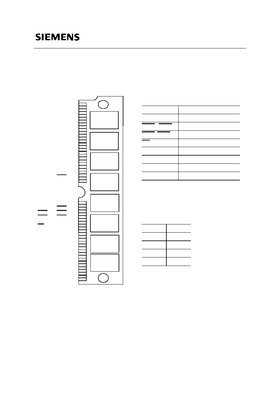
The HYM 364020S/GS-60 is a 16 MByte DRAM module organized as 4 194 304 words by 36-
Bit in a 72-pin single-in-line package comprising eight HYB 5117400BJ 4M
◊
4 DRAMs and four
HYB 514100BJ 4M x 1 DRAMS in 300 mil wide SOJ-packages mounted together with twelve 0.2
µ
F
ceramic decoupling capacitors on a PC board.
The HYM 364020S/GS-60 can also be used as a 8 388 608 words by 18-bits dynamic RAM module
by means of connecting DQ0 and DQ18, DQ1 and DQ19, DQ2 and DQ20, ... , DQ17 and DQ35,
respectively.
Each HYB 5117400BJ and HYB 514100BJ is described in the data sheet and is fully electrical
tested and processed according to SIEMENS standard quality procedure prior to module assembly.
After assembly onto the board, a further set of electrical tests is performed.
The speed of the module can be detected by the use of four presence detect pins.
The common I/O feature on the HYM 364020S/GS-60 dictates the use of early write cycles.
Ordering Information
Type
Ordering Code
Package
Description
HYM 364020S-60
Q67100-Q2006
L-SIM-72-12
DRAM Module
(access time 60 ns)
HYM 364020GS-60
Q67100-Q982
L-SIM-72-12
DRAM Module
(access time 60 ns)
Semiconductor Group
3
HYM 364020S/GS-60
4M
◊
36-Bit
Pin Configuration
Pin Names
Presence Detect Pins
A0-A10
Address Inputs
DQ0-DQ35
Data Input/Output
CAS0 - CAS3
Column Address Strobe
RAS0, RAS2
Row Address Strobe
WE
Read/Write Input
V
CC
Power (+ 5 V)
V
SS
Ground
PD
Presence Detect Pin
N.C.
No Connection
-60
PD0
V
SS
PD1
N.C.
PD2
N.C.
PD3
N.C.
VSS
1 DQ0
2
DQ18
3 DQ1
4
DQ19
5 DQ2
6
DQ20
7 DQ3
8
DQ21
9 VCC
10
N.C.
11 A0
12
A1
13 A2
14
A3
15 A4
16
A5
17 A6
18
A10
19 DQ4 20
DQ22
21 DQ5 22
DQ23
23 DQ6 24
DQ24
25 DQ7 26
DQ25
27 A7
28
N.C.
29 VCC 30
A8
31 A9
32
N.C.
33 RAS2 34
DQ26
35 DQ8 36
DQ17
37 DQ35 38
VSS
39 CAS0 40
CAS2
41 CAS3 42
CAS1
43 RAS0 44
N.C.
45 N.C. 46
WE
47 N.C. 48
DQ9
49 DQ27 50
DQ10
51 DQ28 52
DQ11
53 DQ29 54
DQ12
55 DQ30 56
DQ13
57 DQ31 58
VCC
59 DQ32 60
DQ14
61 DQ33 62
DQ15
63 DQ34 64
DQ16
65 N.C. 66
PD0
67 PD1 68
PD2
69 PD3 70
N.C.
71 VSS 72
Semiconductor Group
4
HYM 364020S/GS-60
4M
◊
36-Bit
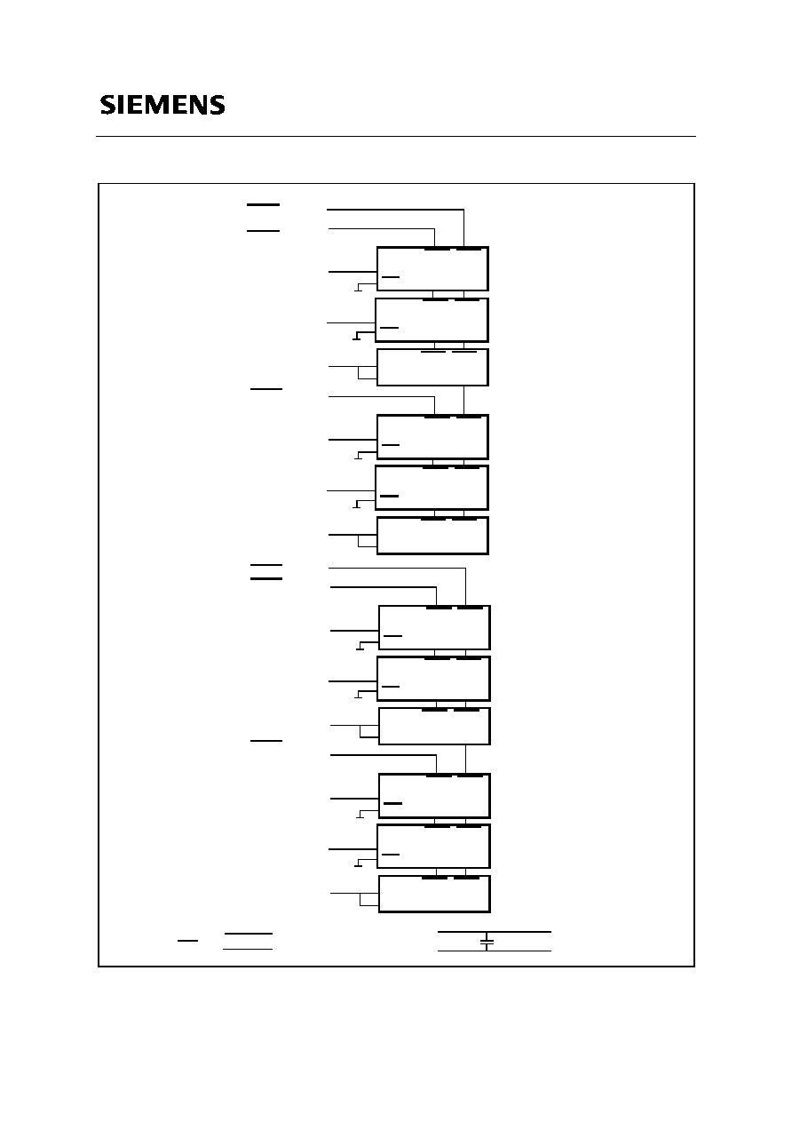
Block Diagram
CAS RAS
I/O1-I/O4
OE
CAS RAS
Di
Do
CAS RAS
I/O1-I/O4
OE
CAS RAS
I/O1-I/O4
OE
CAS RAS
Di
Do
CAS RAS
I/O1-I/O4
OE
CAS RAS
I/O1-I/O4
OE
CAS RAS
Di
Do
CAS RAS
I/O1-I/O4
OE
CAS RAS
I/O1-I/O4
OE
CAS RAS
Di
Do
CAS RAS
I/O1-I/O4
OE
RAS0
CAS0
DQ0-DQ3
DQ4-DQ7
DQ8
CAS1
DQ9-DQ12
DQ13-DQ16
DQ17
RAS2
CAS2
DQ18-DQ21
DQ22-DQ25
DQ26
CAS3
DQ27-DQ30
DQ31-DQ34
DQ35
D0
D1
M0
D2
D3
M1
D4
D5
M2
D6
D7
M3
D0-D7, M0-M3
D0-D7, M0-M3
A0-A10
WE
C0 - C11
VCC
VSS

Semiconductor Group
5
HYM 364020S/GS-60
4M
◊
36-Bit
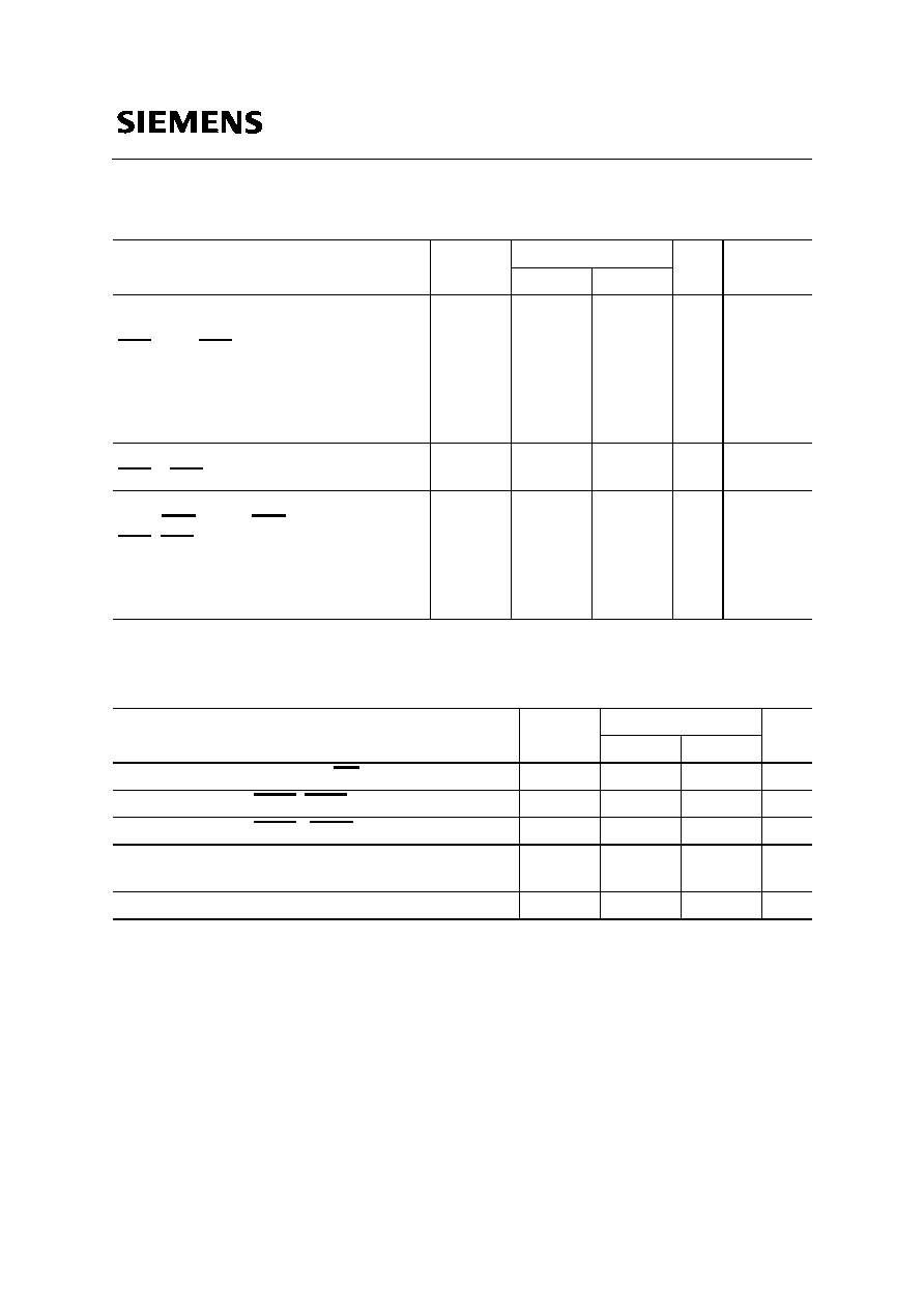
Absolute Maximum Ratings
Operation temperature range .........................................................................................
0 to + 70 ∞C
Storage temperature range.........................................................................................
≠ 55 to 125 ∞C
Input/output voltage ............................................................................ ≠0.5V to min (Vcc+0.5, 7.0) V
Power supply voltage......................................................................................................
≠ 1 to + 7 V
Power dissipation.....................................................................................................................
9.3 W
Data out current (short circuit) ................................................................................................
50 mA
Note:
Stresses above those listed under "Absolute Maximum Ratings" may cause permanent
damage of the device. Exposure to absolute maximum rating conditions for extended periods
may affect device reliability.
DC Characteristics
T
A
= 0 to 70 ∞C,
V
CC
= 5 V
±
10 %
Parameter
Symbol
Limit Values
Unit
Test
Condition
min.
max.
Input high voltage
V
IH
2.4
Vcc+0.5
V
1)
Input low voltage
V
IL
≠ 0.5
0.8
V
1)
Output high voltage (
I
OUT
= ≠ 5 mA)
V
OH
2.4
≠
V
1)
Output low voltage (
I
OUT
= 4.2 mA)
V
OL
≠
0.4
V
1)
Input leakage current
(0 V <
V
IN
< 6.5 V, all other pins = 0 V)
I
I(L)
≠ 20
20
µ
A
1)
Output leakage current
(DO is disabled, 0 V <
V
OUT
< 5.5 V)
I
O(L)
≠ 10
10
µ
A
1)
Average
V
CC
supply current
(RAS, CAS, address cycling,
t
RC
=
t
RC
min)
-60 version
I
CC1
≠
1320
mA
2),3),4)
Standby
V
CC
supply current
(RAS = CAS =
V
IH
)
I
CC2
≠
24
mA
Average
V
CC
supply current
during RAS only refresh cycles
(RAS cycling, CAS =
V
IH
,
t
RC
=
t
RC
min)
-60 version
I
CC3
≠
1320
mA
2),4)
Semiconductor Group
6
HYM 364020S/GS-60
4M
◊
36-Bit
DC Characteristics
1)
(cont'd)
Capacitance
T
A
= 0 to 70 ∞C,
V
CC
= 5 V
±
10 %,
f
= 1 MHz
Parameter
Symbol
Limit Values
Unit
Test
Condition
min.
max.
Average
V
CC
supply current
during fast page mode
(RAS =
V
IL
, CAS, address cycling,
t
PC
=
t
PC
min)
-60 version
I
CC4
≠
920
mA
mA
2),3),4)
Standby
V
CC
supply current
(RAS = CAS =
V
CC
≠ 0.2 V)
I
CC5
≠
12
mA
Average
V
CC
supply current
during CAS-before-RAS refresh mode
(RAS, CAS cycling,
t
RC
=
t
RC
min)
-60 version
I
CC6
≠
2),4)
Parameter
Symbol
Limit Values
Unit
min.
max.
Input capacitance (A0 to A10, WE)
C
I1
≠
75
pF
Input capacitance (RAS0, RAS2)
C
I2
≠
45
pF
Input capacitance (CAS0 - CAS3)
C
I3
≠
25
pF
I/O capacitance
(DQ0-DQ7,DQ9-DQ16,DQ18-DQ25,DQ27-DQ34)
C
IO1
≠
15
pF
I/O capacitance (DQ8,DQ17,DQ26,DQ35)
C
IO2
≠
25
pF
Semiconductor Group
7
HYM 364020S/GS-60
4M
◊
36-Bit
AC Characteristics
5)6)
T
A
= 0 to 70 ∞C,
V
CC
= 5 V
±
10 %,
t
T
= 5 ns
Parameter
Symbol
Limit Values
Unit
Note
-60
min.
max.
common parameters
Random read or write cycle time
t
RC
110
≠
ns
RAS precharge time
t
RP
40
≠
ns
RAS pulse width
t
RAS
60
10k
ns
CAS pulse width
t
CAS
15
10k
ns
Row address setup time
t
ASR
0
≠
ns
Row address hold time
t
RAH
10
≠
ns
Column address setup time
t
ASC
0
≠
ns
Column address hold time
t
CAH
15
≠
ns
RAS to CAS delay time
t
RCD
20
45
RAS to column address delay time
t
RAD
15
30
ns
RAS hold time
t
RSH
15
≠
ns
CAS hold time
t
CSH
60
≠
ns
CAS to RAS precharge time
t
CRP
5
≠
ns
Transition time (rise and fall)
t
T
3
50
ns
7
Refresh period
t
REF
≠
32
ms
Read Cycle
Access time from RAS
t
RAC
≠
60
ns
8, 9
Access time from CAS
t
CAC
≠
15
ns
8, 9
Access time from column address
t
AA
≠
30
ns
8,10
Column address to RAS lead time
t
RAL
30
≠
ns
Read command setup time
t
RCS
0
≠
ns
Read command hold time
t
RCH
0
≠
ns
11
Read command hold time referenced to
RAS
t
RRH
0
≠
ns
11
CAS to output in low-Z
t
CLZ
0
≠
ns
8
Output buffer turn-off delay
t
OFF
0
15
ns
12
Semiconductor Group
8
HYM 364020S/GS-60
4M
◊
36-Bit
Early Write Cycle
Write command hold time
t
WCH
10
≠
ns
Write command pulse width
t
WP
10
≠
ns
Write command setup time
t
WCS
0
≠
ns
13
Write command to RAS lead time
t
RWL
15
≠
ns
Write command to CAS lead time
t
CWL
15
≠
ns
Data setup time
t
DS
0
≠
ns
14
Data hold time
t
DH
10
≠
ns
14
Fast Page Mode Cycle
Fast page mode cycle time
t
PC
40
≠
ns
CAS precharge time
t
CP
10
≠
ns
Access time from CAS precharge
t
CPA
≠
35
ns
7
RAS pulse width
t
RAS
60
200k ns
CAS precharge to RAS Delay
t
RHCP
35
≠
ns
CAS-before-RAS Refresh Cycle
CAS setup time
t
CSR
10
≠
ns
CAS hold time
t
CHR
10
≠
ns
RAS to CAS precharge time
t
RPC
5
≠
ns
Write to RAS precharge time
t
WRP
10
≠
ns
Write hold time referenced to RAS
t
WRH
10
≠
ns
AC Characteristics (cont'd)
5)6)
T
A
= 0 to 70 ∞C,
V
CC
= 5 V
±
10 %,
t
T
= 5 ns
Parameter
Symbol
Limit Values
Unit
Note
-60
min.
max.

Semiconductor Group
9
HYM 364020S/GS-60
4M
◊
36-Bit
Notes:
1) All voltages are referenced to VSS.
2) ICC1, ICC3, ICC4 and ICC6 depend on cycle rate.
3) ICC1 and ICC4 depend on output loading. Specified values are measured with the output open.
4) Address can be changed once or less while RAS = VIL. In the case of ICC4 it can be changed once or less
during a fast page mode cycle (tPC).
5) An initial pause of 200 µs is required after power-up followed by 8 RAS cycles of which at least one cycle has
to be a refresh cycle, before proper device operation is achieved. In case of using internal refresh counter, a
minimum of 8 CAS-before-RAS initialization cycles instead of 8 RAS cycles are required.
6) AC measurements assume tT = 5 ns.
7) VIH (min.) and VIL (max.) are reference levels for measuring timing of input signals. Transition times are also
measured between VIH and VIL.
8) Measured with a load equivalent to 2 TTL loads and 100 pF.
9) Operation within the tRCD (max.) limit ensures that tRAC (max.) can be met. tRCD (max.) is specified as a
reference point only: If tRCD is greater than the specified tRCD (max.) limit, then access time is controlled by
tCAC.
10)Operation within the tRAD (max.) limit ensures that tRAC (max.) can be met. tRAD (max.) is specified as a
reference point only: If tRAD is greater than the specified tRAD (max.) limit, then access time is controlled by
tAA.
11)Either tRCH or tRRH must be satisfied for a read cycle.
12)tOFF (max.) define the time at which the outputs achieve the open-circuit condition and are not referenced to
output voltage levels
.
13)tWCS is not a restrictive operating parameter. This is included in the data sheet as electrical characteristics
only. If tWCS > tWCS (min.), the cycle is an early write cycle and the I/O pin will remain open-circuit (high
impedance) through the entire cycle.
14)These parameters are referenced to the CAS leading edge.
Semiconductor Group
10
HYM 364020S/GS-60
4M
◊
36-Bit
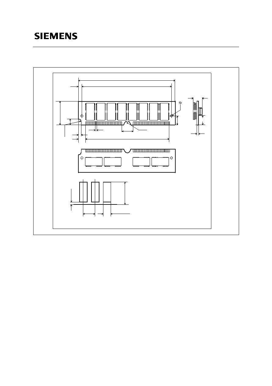
Package Outline
Module Package, L-SIM-72-12
(Single in-Line Memory Module)
GLS05835
107.95
101.19
3.18
6.35
R 1.57
1.27
10.16
2.03
6.35
3.38
6.35
R1.57
Detail of Contacts
1.27
1.04
2.54 min
0.25 max
Tolerances : +/- 0.13 unless otherwise specified
95.25
+/- 0.05
+/- 0.05
+/- 0.05
+/- 0.05
1.27
+0.10
-0.08
7.23 min
8.89 max
FRONT SIDE
BACK SIDE
Frontside : 4Mx4 DRAMs
Backside : 4Mx1 DRAMs
L-SIM7212.DRW/WMF
22.86