
ICs for Communications
Joint Audio Decoder-Encoder for Analog Videophone
JADE AN
PSB 7230 Version 2.1
Data Sheet 1998-07-01
DS 1

For questions on technology, delivery and prices please contact the Semiconductor Group Offices
in Germany or the Siemens Companies and Representatives worldwide: see our webpage at
http://www.siemens.de/semiconductor/communication
PSB 7230
Revision History:
Current Version: 1998-07-01
Previous Version: Prelimiinary Data Sheet 02.97 (V 1.2)
Page
(in previous
Version)
Page
(in current
Version)
Subjects (major changes since last revision)
Edition 1998-07-01
Published by Siemens AG,
HL SP,
Balanstraþe 73,
81541 M¸nchen
©
Siemens AG 1998.
All Rights Reserved.
Attention please!
As far as patents or other rights of third parties are concerned, liability is only assumed for components, not for
applications, processes and circuits implemented within components or assemblies.
The information describes the type of component and shall not be considered as assured characteristics.
Terms of delivery and rights to change design reserved.
Due to technical requirements components may contain dangerous substances. For information on the types in
question please contact your nearest Siemens Office, Semiconductor Group.
Siemens AG is an approved CECC manufacturer.
Packing
Please use the recycling operators known to you. We can also help you ≠ get in touch with your nearest sales
office. By agreement we will take packing material back, if it is sorted. You must bear the costs of transport.
For packing material that is returned to us unsorted or which we are not obliged to accept, we shall have to invoice
you for any costs incurred.
Components used in life-support devices or systems must be expressly authorized for such purpose!
Critical components
1
of the Semiconductor Group of Siemens AG, may only be used in life-support devices or
systems
2
with the express written approval of the Semiconductor Group of Siemens AG.
1 A critical component is a component used in a life-support device or system whose failure can reasonably be
expected to cause the failure of that life-support device or system, or to affect its safety or effectiveness of that
device or system.
2 Life support devices or systems are intended (a) to be implanted in the human body, or (b) to support and/or
maintain and sustain human life. If they fail, it is reasonable to assume that the health of the user may be en-
dangered.
IOM
Æ
, IOM
Æ
-1, IOM
Æ
-2, SICOFI
Æ
, SICOFI
Æ
-2, SICOFI
Æ
-4, SICOFI
Æ
-4
µ
C, SLICOFI
Æ
, ARCOFI
Æ
, ARCOFI
Æ
-BA,
ARCOFI
Æ
-SP, EPIC
Æ
-1, EPIC
Æ
-S, ELIC
Æ
, IPAT
Æ
-2, ITAC
Æ
, ISAC
Æ
-S, ISAC
Æ
-S TE, ISAC
Æ
-P, ISAC
Æ
-P TE, IDEC
Æ
,
SICAT
Æ
, OCTAT
Æ
-P, QUAT
Æ
-S are registered trademarks of Siemens AG.
MUSAC
TM
-A, FALC
TM
54, IWE
TM
, SARE
TM
, UTPT
TM
, ASM
TM
, ASP
TM
, DigiTape
TM
are trademarks of Siemens AG.

PSB 7230
Table of Contents
Page
Semiconductor Group
3
Data Sheet 1998-07-01
1
Introduction . . . . . . . . . . . . . . . . . . . . . . . . . . . . . . . . . . . . . . . . . . . . . . . . .5
1.1
Feature List . . . . . . . . . . . . . . . . . . . . . . . . . . . . . . . . . . . . . . . . . . . . . . . . . .5
1.2
Overview . . . . . . . . . . . . . . . . . . . . . . . . . . . . . . . . . . . . . . . . . . . . . . . . . . . .6
1.3
Logic Symbol . . . . . . . . . . . . . . . . . . . . . . . . . . . . . . . . . . . . . . . . . . . . . . . . .8
1.4
Pin Configuration . . . . . . . . . . . . . . . . . . . . . . . . . . . . . . . . . . . . . . . . . . . . . .9
1.5
Pin Description . . . . . . . . . . . . . . . . . . . . . . . . . . . . . . . . . . . . . . . . . . . . . . .10
1.6
System Integration . . . . . . . . . . . . . . . . . . . . . . . . . . . . . . . . . . . . . . . . . . . .16
1.6.1
H.324 Desktop Videoconferencing Solution for POTS . . . . . . . . . . . . . .17
1.6.2
Low Cost H.324 Desktop Videoconferencing with Software Video . . . . .19
1.6.3
LAN Videoconferencing . . . . . . . . . . . . . . . . . . . . . . . . . . . . . . . . . . . . . .20
1.6.4
Standalone H.324/H.323 Videophone . . . . . . . . . . . . . . . . . . . . . . . . . . .21
1.6.5
Internet Telephone Access in Line Card . . . . . . . . . . . . . . . . . . . . . . . . .22
2
General Architecture and Functions . . . . . . . . . . . . . . . . . . . . . . . . . . . .24
2.1
Architecture . . . . . . . . . . . . . . . . . . . . . . . . . . . . . . . . . . . . . . . . . . . . . . . . .24
2.2
Functions . . . . . . . . . . . . . . . . . . . . . . . . . . . . . . . . . . . . . . . . . . . . . . . . . . .26
2.3
Summary of the Functions . . . . . . . . . . . . . . . . . . . . . . . . . . . . . . . . . . . . . .26
2.3.1
Audio Functions and Supplementary Features . . . . . . . . . . . . . . . . . . . .26
3
Interfaces and Memory Organization . . . . . . . . . . . . . . . . . . . . . . . . . . . .28
3.1
Interfaces . . . . . . . . . . . . . . . . . . . . . . . . . . . . . . . . . . . . . . . . . . . . . . . . . . .28
3.1.1
IOM-2 Interface . . . . . . . . . . . . . . . . . . . . . . . . . . . . . . . . . . . . . . . . . . . .28
3.1.2
Serial Audio Interface . . . . . . . . . . . . . . . . . . . . . . . . . . . . . . . . . . . . . . .30
3.1.3
Parallel Host Interface . . . . . . . . . . . . . . . . . . . . . . . . . . . . . . . . . . . . . . .32
3.1.4
External Memory Interface . . . . . . . . . . . . . . . . . . . . . . . . . . . . . . . . . . . .32
3.1.5
Clock Interface . . . . . . . . . . . . . . . . . . . . . . . . . . . . . . . . . . . . . . . . . . . . .33
3.2
Shared Memories . . . . . . . . . . . . . . . . . . . . . . . . . . . . . . . . . . . . . . . . . . . .34
3.3
Directly Accessible Register Bank . . . . . . . . . . . . . . . . . . . . . . . . . . . . . . . .36
3.3.1
Input/Output Registers . . . . . . . . . . . . . . . . . . . . . . . . . . . . . . . . . . . . . . .36
3.3.2
DSP/Host Com Area . . . . . . . . . . . . . . . . . . . . . . . . . . . . . . . . . . . . . . . .39
3.3.2.1
Access to DSP/Host Com Area . . . . . . . . . . . . . . . . . . . . . . . . . . . . . .39
3.4
Mailbox . . . . . . . . . . . . . . . . . . . . . . . . . . . . . . . . . . . . . . . . . . . . . . . . . . . .44
3.4.1
DSP/Host Com Area with a Demultiplexed Host Interface . . . . . . . . . . .46
4
Functional Blocks . . . . . . . . . . . . . . . . . . . . . . . . . . . . . . . . . . . . . . . . . . .49
4.1
Oscillator and Baud Rate Generator . . . . . . . . . . . . . . . . . . . . . . . . . . . . . .49
4.2
Audio and Data Reception/Transmission . . . . . . . . . . . . . . . . . . . . . . . . . .52
4.3
Serial Data Controller . . . . . . . . . . . . . . . . . . . . . . . . . . . . . . . . . . . . . . . . .64
4.4
IOM-2 Functions . . . . . . . . . . . . . . . . . . . . . . . . . . . . . . . . . . . . . . . . . . . . .67
4.4.1
Monitor Channel Protocol . . . . . . . . . . . . . . . . . . . . . . . . . . . . . . . . . . . .68
4.4.2
C/I Channel . . . . . . . . . . . . . . . . . . . . . . . . . . . . . . . . . . . . . . . . . . . . . . .74
4.5
Programming Indirectly Accessible Registers . . . . . . . . . . . . . . . . . . . . . . .77
4.5.1
Programming via Parallel Host Interface . . . . . . . . . . . . . . . . . . . . . . . . .77

PSB 7230
Table of Contents
Page
Semiconductor Group
4
Data Sheet 1998-07-01
5
Register Description . . . . . . . . . . . . . . . . . . . . . . . . . . . . . . . . . . . . . . . . .78
5.1
Interrupt Structure . . . . . . . . . . . . . . . . . . . . . . . . . . . . . . . . . . . . . . . . . . . .78
5.2
Interrupt Status Registers . . . . . . . . . . . . . . . . . . . . . . . . . . . . . . . . . . . . . .79
5.3
Indirectly Accessible Configuration and Control Registers . . . . . . . . . . . . .82
5.4
Serial Data Controller Registers . . . . . . . . . . . . . . . . . . . . . . . . . . . . . . . .101
6
Firmware Features . . . . . . . . . . . . . . . . . . . . . . . . . . . . . . . . . . . . . . . . . .113
6.1
Basic Functions . . . . . . . . . . . . . . . . . . . . . . . . . . . . . . . . . . . . . . . . . . . . .114
6.1.1
Firmware Version Number . . . . . . . . . . . . . . . . . . . . . . . . . . . . . . . . . . .114
6.1.2
Software Reset . . . . . . . . . . . . . . . . . . . . . . . . . . . . . . . . . . . . . . . . . . .115
6.1.3
Power Down Command . . . . . . . . . . . . . . . . . . . . . . . . . . . . . . . . . . . . .116
6.2
Audio Interfaces . . . . . . . . . . . . . . . . . . . . . . . . . . . . . . . . . . . . . . . . . . . . .117
6.2.1
Compressed Audio Protocols and Control of JADE AN . . . . . . . . . . . .119
6.2.1.1
Outband Control of JADE AN . . . . . . . . . . . . . . . . . . . . . . . . . . . . . .119
6.2.1.2
Compressed Audio Protocol with Outband Control . . . . . . . . . . . . . .130
6.2.1.3
Compressed Audio Protocol with Inband Control . . . . . . . . . . . . . . .132
6.2.1.4
Control Pipeline . . . . . . . . . . . . . . . . . . . . . . . . . . . . . . . . . . . . . . . . .138
6.2.2
Uncompressed Data Protocol . . . . . . . . . . . . . . . . . . . . . . . . . . . . . . . .144
6.2.3
Audio Interface Timings . . . . . . . . . . . . . . . . . . . . . . . . . . . . . . . . . . . . .145
6.2.3.1
Uncompressed Data: Host IF, Compressed Data: Host IF . . . . . . . .145
6.2.3.2
Uncompressed Data: IOM IF, Compressed Data: Host IF . . . . . . . .153
6.2.3.3
Uncompressed Data: IOM IF, Compressed Data: Serial Audio Interface
(SAI) 162
7
Electrical Specification . . . . . . . . . . . . . . . . . . . . . . . . . . . . . . . . . . . . . .165
7.1
Absolute Maximum Ratings . . . . . . . . . . . . . . . . . . . . . . . . . . . . . . . . . . . .165
7.2
Operating Conditions . . . . . . . . . . . . . . . . . . . . . . . . . . . . . . . . . . . . . . . . .165
7.3
DC Characteristics . . . . . . . . . . . . . . . . . . . . . . . . . . . . . . . . . . . . . . . . . . .165
7.4
Capacitances . . . . . . . . . . . . . . . . . . . . . . . . . . . . . . . . . . . . . . . . . . . . . . .167
7.5
Oscillator Circuit . . . . . . . . . . . . . . . . . . . . . . . . . . . . . . . . . . . . . . . . . . . . .167
7.6
XTAL 1,2 Recommended Typical Crystal Parameters . . . . . . . . . . . . . . .167
7.7
AC Characteristics . . . . . . . . . . . . . . . . . . . . . . . . . . . . . . . . . . . . . . . . . . .168
7.7.1
Testing Waveform . . . . . . . . . . . . . . . . . . . . . . . . . . . . . . . . . . . . . . . . .168
7.7.2
Parallel Host Interface Timing . . . . . . . . . . . . . . . . . . . . . . . . . . . . . . . .168
7.7.3
IOM-2 Interface Timing . . . . . . . . . . . . . . . . . . . . . . . . . . . . . . . . . . . . .172
7.7.4
Serial Audio Interface Timing . . . . . . . . . . . . . . . . . . . . . . . . . . . . . . . . .176
7.7.5
External Memory Interface . . . . . . . . . . . . . . . . . . . . . . . . . . . . . . . . . . .178
8
Package Outlines . . . . . . . . . . . . . . . . . . . . . . . . . . . . . . . . . . . . . . . . . . .179

P-TQFP-100
Semiconductor Group
5
Data Sheet 1998-07-01
Joint Audio Decoder-Encoder for Analog Videophone
JADE AN
PSB 7230
Version 2.1
Type
Ordering Code
Package
PSB 7230
Q67101-H6864
P-TQFP-100
1
Introduction
1.1
Feature List
Functions
≠ G.723 V5.1 Compression/Decompression (6.3,
5.3 Kbit/s)
≠ Accepts/outputs uncompressed audio in 8-bit PCM
A/
µ
law or 16-bit linear format
≠ G.711 Compression/Decompression (64 Kbit/s)
≠ Uncompressed/compressed audio switchable between different interface
combinations (IOM
Æ
/Serial Audio Interface, IOM/Host, Host/Host)
≠ Inband controlled H.221/H.223 oriented audio protocol, e.g. for direct serial
connection to Videocodec (VCP of 8
◊
8 Inc., formerly IIT Inc.) as well as host based
solutions
≠ Outband controlled audio protocol with optimized data rate
≠ Stable reaction on interrupt handshake timing violations of e.g. a slow host
(Windows
Æ
PC)
System On-Chip Functions
≠ One universal serial transparent data controller
≠ IOM-2 Monitor and C/I channels
≠ Generation of programmable system clock output
Interfaces
≠ 4-line IOM-2/PCM interface (programmable master or slave)
≠ 5-line serial audio interface, e.g. for connection to Videocodec/H.221/223 processor
≠ Parallel 8-bit Host interface
≠ 4-line general purpose interface

PSB 7230
Introduction
Semiconductor Group
6
Data Sheet 1998-07-01
Control
≠ Programmable via Parallel Host Interface
≠ Operating parameters and mode settings via a register bank
≠ Access to audio channels and serial transparent data controller from DSP or an
external Host
≠ Interface to external software via a full-duplex 256-byte on-chip mailbox
≠ H.221/H.223 oriented inband configuration/mode switching
General
≠ Supply voltage: 3.0 - 3.6 V
≠ Additional 4.5 to 5.5 V supply for connection to 5 V systems without external
components
≠ Ambient temperature range 0
∞
C to + 70
∞
C
≠ P-TQFP-100 package
1.2
Overview
The PSB 7230 Joint Audio Decoder Encoder for Analog Videophones (JADE AN) is a
device which implements voice compression algorithms using the Algebraic Code
Excited Linear Prediction (ACELP) and the Multi-Pulse Maximum Likelihood
Quantization (MP-MLQ) standard as defined in the ITU-T G.723 Recommendation. In
addition G.711 PCM audio coding is also supported.
Thus, in G.723 mode it compresses the PCM (8 bit A-/
µ
-law) or 16 bit linear voice signal
into 5.3 Kbit/s (ACELP) or 6.3 Kbit/s (MP-MLQ) bit stream, and vice versa. The
implementation complies with the newest ITU-T C-code V5.1 and includes the G.723
Annex A (Voice Activity Detection and Comfort Noise Generation).
The JADE AN finds applications in
≠ Analog Videophones (H.324)
≠ Networks (e.g. LANs) for packetized voice (H.323)
≠ Video Conference Systems
≠ Corporate Network voice concentrators, multiplexers and gateways
≠ Data-over-voice and Voice-over-data terminals.
Other potential application areas are:
≠ Networks (e.g. LANs) for packetized voice
≠ Digital Added Main-Line (DAML) & Digital Circuit Multiplication Equipment (DCME)
≠ Voice storage e.g. in PC based applications
≠ Message recording and distribution.
The interfaces of the JADE allow a seamless integration into IOM-2 based systems. After
the circuit is set up in the proper mode of operation and parameter settings are
programmed by a controlling software, the circuit runs independently of the rest of the

PSB 7230
Introduction
Semiconductor Group
7
Data Sheet 1998-07-01
system. Status and control information to/from the JADE can be transferred either
inband the compressed audio data via the corresponding selected interface or outband
using an 8-bit parallel host interface.
The audio frontend data can be exchanged either through the host interface or the IOM-2
interface. In the latter case the Siemens ARCOFI SP can be connected providing
half-duplex handsfree or a Siemens ACE (acoustic echo canceller circuit) together with
an ARCOFI BA providing full duplex handsfree.
The default configuration of the JADE is such, that in a videoconferencing system using
the 8x8 (formerly IIT) VCP (Video Codec and Multimedia Communications Processor)
the Siemens PSB 7230 can work standalone without the need of external initialization.
I.e., no host is needed in this case and the full communication is automatically started
between the VCP and the Siemens PSB 7230.
The voice compression algorithms are implemented by an embedded 16-bit fixed point
Digital Signal Processor with all memories internal and no external memory needed.
Integration of these and other features, as well as perfectly matched interfaces with other
ICs allows for the implementation of highly optimized, low cost system solutions e.g. for
Videophones, Data-over-voice and Channel Multiplexing equipment.
For system integration, a serial data channel is implemented which can be serviced by
an attached host (or the on-chip DSP). System functions and communication between
the chip and an external controller is supported by a full-duplex 256-byte on-chip mailbox
communication memory.
The circuit is offered in a Quad Flat Pack package with 100 pins (P-TQFP-100: size
14
◊
14 mm, pitch 0.5 mm, height 1.4 mm).
Note: This Data Sheet gives a thorough description of the functions and hardware that
forms the base of PSB 7230. It includes information that is not needed for the
PSB 7230 as a `ready to use plug and play' G.723/G.711 audio compression
device.

PSB 7230
Introduction
Semiconductor Group
8
Data Sheet 1998-07-01
1.3
Logic Symbol
Figure 1
SC L K
SR
ST
R F S
T FS
DD
DU
DC L
FSC
RESET
CA (0: 15)
CD(0: 15)
C WR#
CR D#
Serial
Audio
Interface
IOM -2
Int erf ace
Ex ternal Mem ory Interface
CD S#
XTAL 1
PSB 7230
XTA L2
C PS#
CS#
Parallel Hos t Int erf ac e
INT#
AD (0: 7)
R D#
(DS#)
WR#
(R /W#)
AL E
GP IO Interfac e
VD D
VS S
VD DA P, VDD P
Pow er
Supply
CL KO
Sy s tem
Cloc k
Int erface
EA #
INT R#
SIO
CM1
V SSA, V SSAP
VD DA
GPIO(0 :3)
A (0: 3)

PSB 7230
Introduction
Semiconductor Group
9
Data Sheet 1998-07-01
1.4
Pin Configuration
Figure 2
PSB 7230
P-TQFP-100
1
26
51
7 6
SCL K
ALE
CS#
RD#
WR#
AD7
AD6
AD5
AD4
VDDP
VSS
VDD
AD3
AD2
AD1
AD0
INTR#
INT#
A2
FSC
DCL
DU
DD
CA1 5
CD15
CA
1
4
CD
1
4
V
DDP
VS
S
CA
1
3
CD
1
3
CA
1
2
CD
1
2
VD
D
VS
S
VD
D
CA
1
1
CD
1
1
CA
1
0
CD
1
0
VD
D
VS
S
EA
#
CD
S
#
CP
S
#
CWR
#
CR
D#
CA
9
CD
9
CA
8
CA 0
CD1
CA 1
VSS
VDDP
CD2
CA 2
CD3
CA 3
VSS
VDD
CD4
CA 4
CD5
CA 5
VDD
VSS
VDD
CD6
CA 6
CD7
CA 7
VSS
VDD
CD8
SR
ST
RF
S
TF
S
A3
CM
1
VS
S
VD
D
VS
SA
XT
AL
2
XT
AL
1
VD
D
A
VS
SA
P
VD
D
A
P
CL
K
O
SI
O
RE
S
E
T
A1
A0
GP3
GP2
GP1
GP0
VS
S
CD
0

PSB 7230
Introduction
Semiconductor Group
10
Data Sheet 1998-07-01
1.5
Pin Description
Table 1
Parallel Host Interface
Pin No. Symbol Function Descriptions
16
AD0
I/O
Multiplexed Bus Mode: Address/Data Bus. Transfers
addresses from the host to JADE and data between the
host and the JADE
Demultiplexed Bus Mode: Data bus. Transfers data
between the host and the JADE
15
AD1
I/O
14
AD2
I/O
13
AD3
I/O
9
AD4
I/O
8
AD5
I/O
7
AD6
I/O
6
AD7
I/O
4
DS
I
Data Strobe.
The rising edge marks the end of a valid read or write
operation (Motorola bus mode).
RD
I
Read.
This signal indicates a read operation (Siemens/Intel
bus mode).
5
R/W
I
Read/Write.
A 1 ("high") identifies a valid host access as a read
operation. A 0 identifies a valid host access as a write
operation (Motorola bus mode)
WR
I
Write.
This signal indicates a write operation (Siemens/Intel
bus mode).
3
CS
I
Chip Select.
2
ALE
I
Address Latch Enable.
A "high" on this line indicates an address on AD(0:7)
(multipexed bus mode only). ALE also selects the
interface mode
82
A0
I
Address Bits A(0:3) (demultiplexed bus type)
83
A1
I
19
A2
I
96
A3
I

PSB 7230
Introduction
Semiconductor Group
11
Data Sheet 1998-07-01
17
INTR
O (OD)
Interrupt Real-time.
Interrupt output line for high priority interrupt status
(serial audio receive/transmit, serial HDLC data
receive/transmit data) to host.
18
INT
O (OD)
Interrupt Request.
Interrupt output line for all other interrupt states.
Table 2
IOM-2 Interface
Pin No. Symbol Function Descriptions
23
DD
I/O(OD)
Data Downstream on IOM-2/PCM interface.
22
DU
I/O(OD)
Data Upstream on IOM-2/PCM interface.
21
DCL
I/O(OD)
Data Clock.
Clock frequency is twice the data rate, or equal to the
data rate.
20
FSC
I/O(OD)
Frame Sync.
Marks the beginning of a physical IOM-2 or PCM frame.
Table 3
Serial Audio Interface
Pin No. Symbol Function Descriptions
1
SCLK
I/O
Serial Clock.
Serial clock for SR and ST.
100
SR
I/O(OD)
Serial Data Receive.
Should be connected to
V
SS
via a pulldown resistor if not
used.
99
ST
I/O(OD)
Serial Data Transmit.
98
RFS
I/O
Audio Receive Frame Sync.
97
TFS
I/O
Audio Transmit Frame Sync.
Table 1
Parallel Host Interface (cont'd)
Pin No. Symbol Function Descriptions

PSB 7230
Introduction
Semiconductor Group
12
Data Sheet 1998-07-01
Table 4
System Clocks
Pin No. Symbol Function Descriptions
90
XTAL1
I
Crystal In or Clock In.
If a crystal is used, it is connected between XTAL1 and
XTAL2. If a clock signal is provided (via an external
oscillator), this signal is input via XTAL1. In this case the
XTAL2 output is to be left non-connected. The XTAL1
input has to be 50% duty cycle and must not exceed the
voltage range between
V
SSA
and
V
DDA
.
91
XTAL2
O
Crystal Out.
Left unconnected if a crystal is not used.
86
CLKO
O
Clock Out.
Output clock of frequency equal to the internal frequency
divided by a programmable factor.
Table 5
External Memory Interface (for Development Purposes only)
Pin No. Symbol Function Descriptions
75
CA0
O
C-Bus Address.
73
CA1
O
Used for addressing ROM or RAM external to the chip.
69
CA2
O
Is to be left NC if not used.
67
CA3
O
63
CA4
O
61
CA5
O
56
CA6
O
54
CA7
O
50
CA8
O
48
CA9
O
39
CA10
O
37
CA11
O
32
CA12
O
30
CA13
O
26
CA14
O
24
CA15
O

PSB 7230
Introduction
Semiconductor Group
13
Data Sheet 1998-07-01
76
CD0
I/O
C-Bus Data.
74
CD1
I/O
Data bus for external ROM or RAM. Is to be left NC if not
used.
70
CD2
I/O
68
CD3
I/O
64
CD4
I/O
62
CD5
I/O
57
CD6
I/O
55
CD7
I/O
51
CD8
I/O
49
CD9
I/O
40
CD10
I/O
38
CD11
I/O
33
CD12
I/O
31
CD13
I/O
27
CD14
I/O
25
CD15
I/O
43
EA
I
External program Access enable
When "high", an access to program address range
(0000
H
- 7FFF
H
) fetches an instruction from on-chip
ROM. Access to 8000
H
- FFFF
H
addresses external
memory via the External Memory Interface.
When "low", an access to 0000
H
- FFFF
H
(including
0000
H
- 7FFF
H
, normally reserved for on-chip software)
accesses external program memory via the External
Memory Interface.
47
CRD
O
C-Bus Read to external memories.
Left NC if not used.
46
CWR
O
C-Bus Write to external memories.
Left NC if not used.
45
CPS
O
C-Bus Select line for external program memory.
Left NC if not used.
44
CDS
O
C-Bus Select line for external data memory.
Left NC if not used.
Table 5
External Memory Interface (for Development Purposes only) (cont'd)
Pin No. Symbol Function Descriptions

PSB 7230
Introduction
Semiconductor Group
14
Data Sheet 1998-07-01
Table 6
General Control
Pin No. Symbol Function Descriptions
95
CM1
I
Clock Mode
Selects the option for the generation of the DSP internal
working clock.
85
SIO
I/O
Serial I/O line.
When programmed as input, a rising or falling
(selectable) edge on this line may generate a maskable
interrupt INT (host) or INT1 (DSP).
When programmed as output, its state is directly
controlled by the DSP or the host.
84
RESET
I
Reset input. Reset time: > 1 ms.
Table 7
General Purpose I/O Interface
Pin No. Symbol Function Descriptions
81
GP0
I/O (OD)
General purpose I/O pins
80
GP1
I/O(OD)
79
GP2
I/O(OD)
78
GP3
I/O(OD)
Table 8
Power Supply
Pin No. Symbol Function Descriptions
11
V
SS
I
Ground (common to
V
DD
and
V
DDP
)
.
29
V
SS
I
35
V
SS
I
42
V
SS
I
53
V
SS
I
59
V
SS
I
66
V
SS
I
72
V
SS
I
77
V
SS
I
94
V
SS
I

PSB 7230
Introduction
Semiconductor Group
15
Data Sheet 1998-07-01
12
V
DD
I
Positive power supply voltage (3.0 - 3.6 V).
36
V
DD
I
60
V
DD
I
93
V
DD
I
34
V
DD
I
41
V
DD
I
52
V
DD
I
58
V
DD
I
65
V
DD
I
10
V
DDP
I
Positive power supply voltage (4.5 - 5.5 V) for external
interfaces.
28
V
DDP
I
71
V
DDP
I
89
V
DDA
I
Separate positive power supply voltage (3.0 - 3.6 V) for
Clock Generation Unit (Oscillator).
92
V
SSA
I
Separate Ground (0 V) for Clock Generation Unit
(Oscillator).
87
V
DDAP
I
Separate positive power supply voltage (3.0 - 3.6 V) for
Clock Generation Unit (PLL).
The power supply for the PLL requires pin 87 connected
to
V
DDAP
. In former versions of the JADE family pin 87
was connected to
V
DDP
88
V
SSAP
I
Separate Ground (0 V) for Clock Generation Unit (PLL)
Table 8
Power Supply (cont'd)
Pin No. Symbol Function Descriptions

PSB 7230
Introduction
Semiconductor Group
16
Data Sheet 1998-07-01
1.6
System Integration
Example of integration in videophones for analog telephone line:
The first example represents a low-cost solution for a desktop stand-alone videophone
that connects to an analog telephone line.
The analog telephone line can carry up to 28.8 Kbit/s using a V.34 modem or 33.6 Kbit/s
using a V.34bis modem.
The general aspects of videotelephony over analog telephone lines are covered by
ITU-T H.324 recommendations. The video is compressed according to the H.263
recommendation.
The compressed video and audio signals are multiplexed together with additional control
information into a single communication link. The multiplexing is specified by the H.223
recommendation (see Figure 3).
Figure 3
In order to make the best possible use of the total bandwidth and obtain the best possible
video quality, the audio should require only a small fraction of the total data rate. This is
made possible by using parametric compression techniques such as ACELP (5.3 Kbit/s)
or MP-MLQ (6.3 Kbit/s). Above all, the corresponding norm (G.723) is an internationally
adopted standard, so that compatibility between equipment from different manufacturers
is ensured.

PSB 7230
Introduction
Semiconductor Group
17
Data Sheet 1998-07-01
1.6.1
H.324 Desktop Videoconferencing Solution for POTS
An H.324 desktop videoconferencing solution for POTS (plain old telephone system) line
as a PCI card for commercial PC's is shown in Figure 4.
Figure 4
The connection to the POTS line can be done either by an on-board modem or an
external V.34+ modem that is capable of synchronous data transfer. In the case of the
modem on board, the videophone can be regarded as an add-on modem feature.
The JADE AN and the video codec chip (e.g. the Video Communication Processor "VCP"
from 8
◊
8 Inc.) constitute the heart of the videophone.
Both (together with the modem) are connected to the PC via a PCI Bus Interface (e.g.
the "VPIC" of 8
◊
8 Inc.).
The JADE AN compresses/decompresses audio according to the ITU-T standards
G.723 (5.3 and 6.3 Kbit/s) and G.711 (used in e.g. LAN applications) and runs a fully
inband controlled protocol on the interface to the video codec. It receives/transmits
uncompressed audio via the IOM-2 interface from/to the ARCOFI-SP. The JADE AN is
setup for this application automatically after a hardware reset, so no additional
initialization by a host is required. Since the JADE AN has all its memories on chip, no
external SRAM needs to be connected.
IOM-2
Host
PCI Bus
Video in
SRAM
Video
Capture
SRAM/DRAM
Video out
PAL/NTSC
Camera
JADE AN
SIEMENS
PSB 7230
ARCOFI-SP
SIEMENS
PSB 2163
MPEG 1
PCI
Bus Interface
Video
Codec
V.34+ Modem *)
(synchronous access)
........
tip/ring
tip/ring
*) either an on-board modem or an external modem may be used
Stereo DAC
optional
ALIS
SIEMENS
PSB 4595/
PSB 4596
ISAR 34
SIEMENS
PSB 7115

PSB 7230
Introduction
Semiconductor Group
18
Data Sheet 1998-07-01
The ARCOFI-SP (Audio Ringing Codec Filter) is a hands-free codec for 3.1 kHz voice
which performs detection and elaborate balancing of the received and transmitted audio
to suppress undesirable effects due to acoustical feedback of the signal from the remote
subscriber. The quality obtained is very close to that of echo-free full duplex
conferencing.
The video is captured by a PAL/NTSC camera and digitized and demodulated e.g. by a
standard SAA7110 which is directly connected to the video processor. Alternatively, a
digital camera may be used, which can be connected directly to the video processor.
The video processor compresses and decompresses video according to the ITU-T
standards H.263 and multiplexes/demultiplexes video, audio and data according to
H.223. The video processor uses DRAMs and SRAMs to store data and program code.
The H.223 multiplexed data stream is either sent via the PCI interface to an external
V.34+ modem or via host or IOM-interface to an on-board modem (e.g. Siemens
ISAR-34 (PSB7115) and ALIS (PSB 4595/4596)). The modem must be able to work in
synchronous mode, i.e. the H.223 multiplexed data shall be applied directly to the V.34+
synchronous data pump. When an external, non-integrated V.34+ modem is utilized,
control between the modem and the terminal shall be via ITU-T V.80.
For the on-board modem the ISAR 34 constitutes the data pump transferring the data
with 33.6 Kbit/s in both directions.
The ALIS chipset substitutes the conventional codec and DAA circuit. Since the ALIS it
is a programmable solution, it can be configured by software to fit the approval
requirements of all different countries, thus one hardware solution can be produced for
all markets over the world. The decoupling between line and modem is done by
capacitors instead of transmformers, thus offering very small size and low cost
implementations.
To achieve "lip synchronization", the audio may be delayed with respect to the video.
This is necessary because of the higher transmission delay caused by the video signal,
due to the elaborate H.263 video compression. A delay of approximately 0.5 seconds is
enough in most practical cases. To make maximum use of the existing memory in the
system, the delay is performed by the video processor with its external RAMs.
When decoding MPEG bitstreams, the audio D/A conversion is provided by a stereo
audio DAC.

PSB 7230
Introduction
Semiconductor Group
19
Data Sheet 1998-07-01
1.6.2
Low Cost H.324 Desktop Videoconferencing with Software
Video
A low-cost solution of the previous board does the video encoding/decoding in software
on the host. See Figure 5 for low-cost H.324 desktop videoconferencing.
Figure 5
The V.34+ modem can be either on board, thus building a modem with additional
videophone functionality, or an existing external modem can be used. For a description
of the ISAR-34 data pump and the ALIS programmable codec and DAA worldwide
solution see Chapter 1.6.1.
The audio compression is done by the JADE AN, thus providing high quality audio
without noise or gaps when the operating system of the host processor is busy. For
example when opening a DOS-Shell in a Microsoft Windows
Æ
operating system, the
JADE AN enables the system to have continous audio without gaps or clicks.
IOM-2
Host
PCI Bus
Video in
Video
Capture
PAL/NTSC
Camera
JADE AN
SIEMENS
PSB 7230
ARCOFI-SP
SIEMENS
PSB 2163
PCI Bus IF
Siemens
SZB 6120
V.34+ Modem *)
(synchronous access)
........
tip/ring
*) either an on-board modem or an external modem may be used
Video Compression
by Software on Host
tip/ring
ALIS
SIEMENS
PSB 4595/
PSB 4596
ISAR 34
SIEMENS
PSB 7115

PSB 7230
Introduction
Semiconductor Group
20
Data Sheet 1998-07-01
1.6.3
LAN Videoconferencing
For videoconferencing over LAN, usually high bandwidth is available, thus resulting in
an advantage of hardware videocoding versus software video coding. In addition, high
audio quality with acoustic echo cancellation is requested. See Figure 6 for a LAN
videoconferencing board.
Figure 6
Since the line connection is off-board, all kinds of connections (ISDN H.320, POTS
H.324 or LAN H.323) can be used with a single board. The LAN standard H.323
implements a correction mechanism for non-guaranteed quality of service, thus enabling
also videoconferencing via Internet.
The audio input/output in this example is done via the Siemens ARCOFI BA (PSB 2161)
and the Siemens ACE (PSB 2170), an acoustic echo canceller which implements two
different algorithms (switchable) for minimum delay and maximum performance.
An MPEG playback possibility is optional in this example and can be skipped to reduce
costs.
Host
PCI Bus
Video in
SRAM
Video
Capture
SRAM/DRAM
Video out
PAL/NTSC
Camera
JADE AN
SIEMENS
PSB 7230
ARCOFI BA
SIEMENS
PSB 2161
Stereo DAC
optional
MPEG 1
PCI
Bus Interface
Video
Codec
LAN
Subscriber
IOM-2
ACE - Acoustic
Echo Canceller
SIEMENS
PSB 2170

PSB 7230
Introduction
Semiconductor Group
21
Data Sheet 1998-07-01
1.6.4
Standalone H.324/H.323 Videophone
The following example shows an H.324 (or H.323) standalone videophone solution for
analog telephone line:
Figure 7
Compared to a PCI plug-in card a microcontroller, keypad and screen need to be added
for a standalone videophone.
The initialization and keyboard control is done by the microcontroller. It substitutes the
tasks of the host processor in the previous examples.
The screen (e.g. standard CCD device) is connected directly to the video codec via a 3
DAC.
The multiplexing of the video and audio bitstreams (H.223 or H.225) can be either done
by the video codec or the microcontroller.
ARCOFI BA
SIEMENS
PSB 2161
ACE - Acoustic
Echo Canceller
SIEMENS
PSB 2170
IOM-2
Host
Video in
Video
Capture
SRAM/DRAM
Video out
PAL/NTSC
Camera
JADE AN
SIEMENS
PSB 7230
Micro-
Controller
Video
Codec
3 DAC
SRAM
EEPROM
Keyboard
1
2
3
4
5
6
7
8
9
*
0
#
F3
F2
F1
F4
tip/ring
ALIS
SIEMENS
PSB 4595/
PSB 4596
ISAR 34
SIEMENS
PSB 7115

PSB 7230
Introduction
Semiconductor Group
22
Data Sheet 1998-07-01
The other components are already known from the previous examples, so please refer
to the above descriptions for details.
1.6.5
Internet Telephone Access in Line Card
Figure 8 shows an internet telephone access implemented in an analog line card of a
common tip/ring line. There is no need for the user to buy a special internet telephone.
With his old equipment he can use the internet for rate-reduced calls to overseas or to
connect to a "true" internet telephone. At the beginning or even before a new call the user
may select between the "standard" tarif via the switching network and a "reduced rate"
tarif transferring speech via a packetized network such as internet.
Since the JADE AN does the voice compression/decompression complying to ITU-T
G.723 standard, it can connect to any other telephone using the same standard (e.g.
Microsoft Netmeeting).
The example below shows a line card with 8 subscribers. The number of JADE AN to
connect to the internet may be selected between 1 and 8 - depending on the statistical
usage of this kind of connection.
Alternatively, an internet access with voice compression can also be implemented in the
switching network. This may offer an even better statistical distribution, thus optimizing
the number of gateways needed.
Figure 8
.
.
.
1
4
8
5
.
.
.
SICOFI-4
Siemens
PEB 2465
SICOFI-4
Siemens
PEB 2465
DU
DD
Switching
Network
...
Internet Gateway
JADE AN
Siemens
PSB 7230
G.723
A-/u-law
or 16-bit
linear
A-/u-law
or 16-bit
linear
A-/u-law
or 16-bit
linear
G.723
G.723
JADE AN
Siemens
PSB 7230
JADE AN
Siemens
PSB 7230
Internet
Line Card

PSB 7230
Introduction
Semiconductor Group
23
Data Sheet 1998-07-01
The same principle may also be used for ISDN lines, thus connecting common ISDN
telephones to internet phones like Microsoft Netmeeting or using the internet for
rate-reduced overseas connections.
Demonstration Board Designs
For Demonstration board designs containing the mentioned components please contact
Siemens.

PSB 7230
General Architecture and Functions
Semiconductor Group
24
Data Sheet 1998-07-01
2
General Architecture and Functions
2.1
Architecture
Figure 9 shows a sketch of the PSB 7230 architecture with its most important functional
modules.
Figure 9
The audio processing of the PSB 7230 is based on a 16-bit fixed point DSP core, SPCF
(Signal Processor Core Fast).
The Clock Generator is responsible for generating the internal clocks for the SPC. A
Baud Rate Generator provides an output clock of programmable rate.
The Parallel Host Interface is used to control the circuit through an associated host via
interrupt handshake procedures. Alternatively, the circuit can be controlled via the Serial
Audio Interface, thus enabling stand-alone applications to be implemented.
Communication between the Host, if used, and the DSP is interrupt supported, via a full-
duplex 64-byte on-chip Communication Memory Mailbox.
BR G
c l ock
g en
IOM/
PCM
Ser ial
A udi o
I/F
Mon, C/I
Control
DS P
Co re
SC LK
SR
ST
R FS
T FS
DD
DU
DC L
G P(0: 3)
Reset
XTAL 1
CL KO
CS#
AD(0:7)
WR#
RD#
AL E
P ar al l el Ho s t In t er f ac e
8 K W data
X-ROM
INTR#
XTAL 2
INT#
SIO
2 K W d ata
X-RAM
32 KW program
ROM
Audio
Serial
Data
Channels
Rec 1
T rm 1
1 KW data
Y-RAM
Mail bo x
256-by tes
1 KW data
X-RA M
Co nfig/Con trol
R egist ers
GPIO
I/F
CA (0:1 5)
CD (0:1 5)
C WR #
CRD #
CD S#
CP S#
Ex ternal Memory Interface

PSB 7230
General Architecture and Functions
Semiconductor Group
25
Data Sheet 1998-07-01
One receive and one transmit audio channel are provided. They are input/output on the
ISDN Oriented Modular (IOM-2) or the Serial Audio Interface (SAI) interfaces in
individually programmable time-slots. These channels are accessed from the DSP and/
or the Parallel Host Interface.
The Serial Data Controller channels can be serviced by the DSP or the Parallel Host
Interface. The serial data for the serial data controller is located in programmable time-
slots on IOM-2 and/or SAI.

PSB 7230
General Architecture and Functions
Semiconductor Group
26
Data Sheet 1998-07-01
2.2
Functions
2.3
Summary of the Functions
The main functions implemented by the PSB 7230 are:
≠ G.723 V5.1 Compression/Decompression (6.3, 5.3 Kbit/s)
≠ G.711 Compression/Decompression (64 Kbit/s)
≠ Accepts/outputs uncompressed audio 8-bit PCM A/
µ
law or 16-bit linear format
≠ Uncompressed/compressed audio switchable between different interface
combinations (IOM/Serial Audio Interface, IOM/Host, Host/Host)
≠ Inband controlled H.221/H.223 oriented audio protocol, e.g. for direct serial
connection to Videocodec (VCP of 8
◊
8 Inc., formerly IIT Inc.)
≠ Outband controlled audio protocol with optimized data rate
≠ Stable reaction on interrupt handshake timing violations of e.g. a slow host
(Windows
Æ
PC)
Details about these functions are given in Chapter 2.3.1.
For more details on the hardware (necessary for a better understanding of some of the
topics described in the present chapter), please refer to the other chapters of this Data
Sheet.
2.3.1
Audio Functions and Supplementary Features
General
The uncompressed/compressed audio is applied to the interfaces as follows:
"Transparent" means that data is received/transmitted in a time-slot without protocol.
Table 9
Uncompressed Audio
Compressed Audio
IOM-2 (transparent)
SAI (H.221/223 oriented audio protocol or
transparent)
IOM-2 (transparent)
Host IF (interrupt handshake protocol with
minimized interrupt load for the host)
Host IF (interrupt handshake protocol)
Host IF (interrupt handshake protocol)

PSB 7230
General Architecture and Functions
Semiconductor Group
27
Data Sheet 1998-07-01
Full Duplex G.711 Encoding/Decoding of one Audio Channel
Audio coding according to ITU-T G.711 recommendation using Pulse Code Modulation
(PCM, 64 Kbit/s). A logarithmic function is used for coding of 8 kHz audio samples, thus
offering a nearly constant S/N over the whole amplitude range. Two different laws are
defined known as A- and
µ
-law.
Full Duplex G.723 Encoding/Decoding of one Audio Channel
Audio coding according to ITU-T G.723 recommendation using Multipulse Maximum
Likelihood Quantization (MP-MLQ, 6.3 Kbit/s) or Algebraic Code Excited Linear
Prediction (ACELP, 5.3 Kbit/s). The high pass filter and the postfilter of the G.723 may
be independently switched on or off. The implementation complies with the newest ITU-T
C-Code V5.1 and contains Voice Activity Detection (VAD), Comfort Noise Generation
(CNG) and Discontinous Transmission (DTX).
Serial H.221/223 Oriented Audio Protocol.
The PSB 7230 supports a serial H.221/223 oriented inband controlled audio protocol for
direct connection to a Videocodec (e.g. VCP of 8
◊
8 Inc.), which means the control data
for compression mode, volume etc. is sent in a header preceeding the compressed data.
This protocol provides an outband synchronization of the audio bit streams by using
block structures for the compressed audio data.

PSB 7230
Interfaces and Memory Organization
Semiconductor Group
28
Data Sheet 1998-07-01
3
Interfaces and Memory Organization
3.1
Interfaces
3.1.1
IOM-2 Interface
Electrical interface
The IOM-2 interface is a 4-wire interface with two data lines (DD and DU, programmable
open drain or push-pull), a data clock line (DCL input/output) and a frame sync signal
(FSC input/output). The data clock is by default equal to twice the data rate ("Double
rate"). However, DCL may be set equal to the data rate ("Single rate") by programming.
In terminal applications, the bit rate on the interface is normally 768 Kbit/s, in line card
applications it is 2048 Kbit/s (for details, see IOM-2 Interface Reference Guide).
However, the data rate may be different (between 16 Kbit/s and 4.096 Mbit/s and the
DCL rate correspondingly between 16 kHz and 4.096 MHz), since the interface can be
considered as a general purpose TDM (Time-Division Multiplex) highway.
The total number of time slots on the interface is not explicitly programmed: instead, the
FSC signal (at repetition rate 8 kHz) always marks the TDM physical frame beginning.
See Figure 10 for both IOM clock rates (CRS = 0/1).
Figure 10

PSB 7230
Interfaces and Memory Organization
Semiconductor Group
29
Data Sheet 1998-07-01
Channels
The following channels may be programmed on the IOM-2 interface: one receive audio
channel, one transmit audio channel, one Monitor channel, two C/I channels, one
receive and one transmit data channel:
The transfer of voice samples is performed with the help of an interrupt with repetition
rate 8 kHz derived from the FSC signal. A double-buffered register is provided for each
channel, accessible from the DSP and from the parallel host interface. The double
buffered register ensures that enough time is always provided for reading and writing
data before an overflow/underflow occurs, independent of the location of the time-slots.
Alternatively, the audio samples can be transferred between the DSP or Host and IOM-2
by using an interrupt generated when a programmable number (1 ... 32) of bits are
shifted out (number independent of the time-slot length on the line).
Outside the time slots where transmission takes place the DU and DD lines are in high
impedance.
DCL
Bits on DU/DD are clocked out with the rising edge of DCL and
latched in with the falling edge of DCL. Frequency 16 kHz to
4.096 MHz.
FSC (8 kHz)
Marks the beginning of the physical frame on DU and DD. The first
bit in the frame is output after the rising edge of FSC. The first bit in
the frame is latched in with the first falling edge after FSC has gone
"high" if CRS = 1, or after the second edge (at 3/4) if CRS = 0.
Audio receive channel
Audio transmit channel
Independently programmable on DD or
DU, with programmable locations (start at
bit 1 ... 512) and lengths (1 ... 32 bits)
w.r.t. FSC
Monitor channel
Programmable on DD(in)/DU(out) or
DD(out)/DU(in), with programmable
time-slot (3rd byte in multiplex 0 ... 15)
after FSC
Two C/I channels
Programmable on DD(in)/DU(out) or
DD(out)/DU(in), with programmable length
(4 or 6 bits) and position (4th byte in
multiplex 0 ... 15) after FSC
Data receive and transmit channels
Independently programmable on DD or
DU, with programmable locations (start at
bit 1 ... 512) and lengths (1 ... 256 bits)
w.r.t. FSC

PSB 7230
Interfaces and Memory Organization
Semiconductor Group
30
Data Sheet 1998-07-01
3.1.2
Serial Audio Interface
The Serial Audio Interface is a generic 5-line serial interface with the following lines:
Figure 11 shows an example where RFS is input and TFS is output.
Figure 11
SCLK
Serial bit clock
Input or Output
SR
Serial Receive
Input/Output
ST
Serial Transmit
Input/Output
RFS
Receive Frame Sync
Input or Output
TFS
Transmit Frame Sync
Input or Output.

PSB 7230
Interfaces and Memory Organization
Semiconductor Group
31
Data Sheet 1998-07-01
SCLK is derived from the chip-internal DSP clock via a programmable baud rate
generator (division factor 1, 2, 3 ... 1024).
The Receive Frame Sync (RFS), when programmed as output, has two selectable
modes of operation:
≠ In the continuous mode (CONT = 1), pulses are continuously generated, separated
by a distance
16
◊
(PRD + 1) bits from each other, where PRD = 0 ... 255.
≠ In the burst mode (CONT = 0), pulses are generated upon command a
programmable number of times (REP + 1 : 1 ... 1024), spaced 16 bits apart from each
other.
The same applies to TFS when it is an output.
SCLK
Input or output
Bits on SR/ST are clocked out with the rising edge of SCLK and latched in with
the falling edge of SCLK. When SCLK is programmed as output, it is derived
from a programmable baud rate generator.
RFS
Input or output
Marks the beginning of the physical frame on SR.
When input:
Sampled with a falling edge of SCLK
When output:
Clocked out with the rising or falling edge of SCLK
(duration = 1 SCLK period).
Repetition rate (continuous mode) or number of
pulses (burst mode) is programmable
TFS
Input or output
Marks the beginning of the physical frame on ST.
When input:
Sampled with a falling edge of SCLK
When output:
Clocked out with the rising or falling edge of SCLK
(duration = 1 SCLK period).
Repetition rate (continuous mode) or number of
pulses (burst mode) is programmable

PSB 7230
Interfaces and Memory Organization
Semiconductor Group
32
Data Sheet 1998-07-01
Channels
3.1.3
Parallel Host Interface
The parallel host interface can be selected to be either of the
1. Motorola type with control signals CS, R/W, DS
2. Siemens/Intel demultiplexed bus type with control signals CS, WR, RD
3. or of the Siemens/Intel multiplexed address/data bus type with control signals CS,
WR, RD, ALE
The selection is performed via pin ALE as follows:
ALE tied to
V
DD
(1)
ALE tied to
V
SS
(2)
Edge on ALE
(3)
The occurence of an edge on ALE, either positive or negative, at any time during the
operation immediately selects the multiplexed bus type. A return to one of the other is
possible only if a hardware reset is issued.
3.1.4
External Memory Interface
The external memory interface allows the connection of both program and data
memories to the PSB 7230. The access to either type of memory is determined by the
signals CPS and CDS, respectively. In standard applications, the external memory
interface used as a program memory interface is normally not needed, but is reserved
for development purposes.
The upper 32k half (8000
H
- FFFF
H
) of the address space is reserved for execution of
software from external memory.
For executing software in the lower address range 0000
H
- 7FFF
H
, a control line EA
(External Access) determines whether program is fetched from internal or external
memory. Thus, in standard applications, the EA line should always be "high".
The DSP program execution can be controlled from the outside by loading the
PC-counter of the DSP via the parallel host interface.
Audio receive and transmit channels
Independently programmable on SR, ST,
DU or DD with programmable locations
(start at bit 1 ... 512) and lengths
(1 ... 32 bits) with respect to RFS/TFS
Data receive and transmit channels
Independently programmable on SR, ST,
DU or DD with programmable locations
(start at bit 1 ... 512) and lengths
(1 ... 256 bits) with respect to RFS/TFS

PSB 7230
Interfaces and Memory Organization
Semiconductor Group
33
Data Sheet 1998-07-01
The external memory interface implements:
≠ protection against reading the internal ROM.
3.1.5
Clock Interface
The chip internal clock is derived from a crystal connected across XTAL1,2 or from an
external clock input via pin XTAL1. Two different clock options are provided, controlled
by the clock mode pin CM1.
These clock modes are:
After reset the pin CLKO outputs a frequency of 7.68 MHz, independent of the selection
of CM1 bit. Alternatively, CLKO can be programmed to output the frequency of a
programmable divider (CKOS bit in register 2002
H
). Thus, a clock of frequency equal to
the internal clock divided by a programmable baud rate factor (1, 2, 3 ... 2
19
) can be
generated.
When using the PLL (CM1 = 0), it is made sure that during reset phase CLKO delivers a
continuous 7.68 MHz clock. When using the non-PLL mode (CM1 = 1) CLKO goes low
while reset phase.
CM1 = 0
The internal clock circuitry generates a frequency 4.5 times the input
on XTAL1(,2). The internal frequency required is 34.56 MHz and is
obtained by providing a frequency of 7.68 MHz on XTAL1 input.
CM1 = 1
The internal frequency is directly input via XTAL1(,2). When using a
crystal, a 34.56 MHz crystal swinging at its basic harmonic has to be
connected to XTAL1,2.

PSB 7230
Interfaces and Memory Organization
Semiconductor Group
34
Data Sheet 1998-07-01
3.2
Shared Memories
Note: The absolute addresses for the different internal register banks and memories are
given here and in the rest of this Data Sheet both as seen from the host and from
the embedded DSP, the latter information being included for the sake of
completeness only.
Directly Accessible Register Bank (DARB)
The Host accesses directly via its 8-bit address bus the so-called Directly Accessible
Register Bank (DARB) located between DSP addresses 3000
H
and 30FF
H
.
Figure 12
This area is in turn divided into four blocks of 64 bytes each according to their functions.
An overview of the functions of these 64-byte areas is given in Figure 13, please refer
also to the appropriate chapters for a detailed description.
1. Locations for reading and writing samples "in real time" from/to the serial interfaces
(IOM-2 and Serial Audio Interface) - Input/Output area
2. Area for communication between the host and the embedded DSP, for programming
parameters and reporting status conditions - DSP/Host Com area
3. Register bank for Serial Data Controller - accessed by host if HHA1 (Configuration bit)
is "1" - SDATA
4. Reserved for future expansion.

PSB 7230
Interfaces and Memory Organization
Semiconductor Group
35
Data Sheet 1998-07-01
Figure 13
Not all the addresses in each of these 64-byte areas are used. The functions of the
register bank are detailed in the following paragraphs.

PSB 7230
Interfaces and Memory Organization
Semiconductor Group
36
Data Sheet 1998-07-01
3.3
Directly Accessible Register Bank
3.3.1
Input/Output Registers
This area contains the locations for receiving/transmitting real-time audio and data
between the serial interfaces (IOM-2 and Serial Audio Interface) and the Host (or
embedded DSP).
The PSB 7230 implements one receive and one transmit audio channel, denoted RC1
and XC1, respectively. Further, one receive and one transmit channel is provided to
access the serial data receiver input data and the serial data transmitter output,
respectively, called HR1 and HX1.
Transfer of audio samples is interrupt supported, whereby two possibilities are provided:
≠ interrupt status generated after a programmable number of bits (1 ... 32) have been
shifted in/out;
≠ interrupt indicating the start of a physical frame (normally at 8 kHz, either from FSC,
RFS or TFS frame sync pulses): in this case the number of significant bits depends
on the time-slot length programmed for that channel on the line (DU/DD/SR/ST).
The interrupt statuses may generate a maskable interrupt on the high priority interrupt
lines INTR (Host) and/or INT0 (embedded DSP), respectively.
RC1, XC1, HR1, HX1 channel registers are located in the address range 00
H
- 3F
H
for
the Host, and in the memory mapped area 3000
H
- 303F
H
for the DSP. The register
banks for the Host and the DSP are physically separate from each other. The read
registers and write registers are physically separate.
The addresses for these registers are such that a 32-bit sample can be accessed from
the DSP via only two 16-bit read/write operations (16-bit data bus). From the Host, the
access is byte by byte (8-bit data bus).
List of Registers
RC1:
32-bit register for audio receive channel 1 (read)
XC1:
32-bit register for audio transmit channel 1 (write)
HRR1:
32-bit register for reading data from Data Receiver input shift register
HRW1:
32-bit register for writing data to be loaded into Data Receiver input
HXR1:
32-bit register for reading data from Data Transmitter output
HXW1:
32-bit register for writing data to Data Transmitter output shift register

PSB 7230
Interfaces and Memory Organization
Semiconductor Group
37
Data Sheet 1998-07-01
Memory Map
Figure 14

PSB 7230
Interfaces and Memory Organization
Semiconductor Group
38
Data Sheet 1998-07-01
Alignment of Data for Audio Channel
The most significant bit is always the first bit received/transmitted. Therefore, if audio is
processed in units of N bits (N programmable between 1 and 32), the alignment of the
data for receive and transmit audio channels in the registers is as shown in Figure 15.
Figure 15
Alignment of Data for Serial Data Channel
In the serial data controller the reception/transmission of most significant or least
significant bit can be selected by control switches (RMSB, XMSB). Nevertheless, for
serial data communication, the convention is that the least significant bit of user data is
received/transmitted first. In order to have an identical format for the data in the serial
controller input/output registers as in the FIFOs, the data is aligned in the registers as
shown below (the available options for data unit sizes when pre/postprocessing data are:
1, 2 or 4 bytes).
Figure 16

PSB 7230
Interfaces and Memory Organization
Semiconductor Group
39
Data Sheet 1998-07-01
3.3.2
DSP/Host Com Area
The DSP/Host communication area contains the registers to support hardware and
software interrupts and special purpose registers that support communication between
the embedded DSP and the Host, in particular for indirect programming of the
Configuration and Control registers from the host (see Figure 16).
3.3.2.1
Access to DSP/Host Com Area
The address mapping in multiplexed mode is given in Table 10.
Table 10
Address Mapping of DSP/Host Com Area (Multiplexed Mode)
DSP
Address
DSP Write
(always
16bit wide)
DSP Read
(always 16
bit wide)
Host
Address
AD0-7
Host Write
(always 8bit
wide
Host Read
(always 8bit
wide)
FF
H
- FE
H
reserved reserved
FD
H
- FC
H
reserved
reserved
77
H
Acknowledge
INT MSB
3076
H
Acknowledge
INT
76
H
Acknowledge
INT LSB
75
H
Interrupt INT
Mask MSB
Interrupt INT
Status MSB
3074
H
Interrupt INT
Mask
Interrupt INT
Status
74
H
Interrupt INT
Mask LSB
Interrupt INT
Status LSB
73
H
Acknowledge
INTR
3072
H
Acknowledge
INTR
71
H
Interrupt
INTR Mask
MSB
Interrupt
INTR Status
MSB
3070
H
Interrupt
INTR Mask
Interrupt
INTR Status
70
H
Interrupt
INTR Mask
LSB
Interrupt
INTR Status
LSB
6C
H
reserved
reserved
6A
H
reserved
reserved

PSB 7230
Interfaces and Memory Organization
Semiconductor Group
40
Data Sheet 1998-07-01
The functions of these registers are described below.
3061
H
Cntrl DSP
Host MSB
Cntrl Host
DSP MSB
61
H
Cntrl Host
DSP MSB
Cntrl DSP
Host MSB
3060
H
Cntrl DSP
Host LSB
Cntrl Host
DSP LSB
60
H
Cntrl Host
DSP LSB
Cntrl DSP
Host LSB
Note: Read and write
accesses to 3060
H
and
3061
H
from the DSP
are 8bit wide only.
3058
H
IND Interrupt
Status
INDB (LSBit)
58
H
INDB (LSBit)
IND Interrupt
Status
3050
H
INHB (LSBit)
INH Interrupt
Status
50
H
INH Interrupt
Status
INHB(LSBit)
4C
H
Mailbox IO
write
Mailbox IO
read
4A
H
Mailbox write address
48
H
Mailbix read address
47
H
Ext. Memory
Data high
46
H
Ext. Memory
Data low
45
H
Ext. Memory
Addr high
44
H
Ext. Memory
Addr low
3041
H
Reg Data
DSP
Host
Reg Data
Host
DSP
41
H
Reg Data
Host
DSP
Reg Data
DSP
Host
3040
H
RDY(LSBit)
Conf/Cont
Reg Address
40
H
Conf/Cont
Reg Address
RDY(LSBit)
Table 10
Address Mapping of DSP/Host Com Area (Multiplexed Mode) (cont'd)
DSP
Address
DSP Write
(always
16bit wide)
DSP Read
(always 16
bit wide)
Host
Address
AD0-7
Host Write
(always 8bit
wide
Host Read
(always 8bit
wide)

PSB 7230
Interfaces and Memory Organization
Semiconductor Group
41
Data Sheet 1998-07-01
Indirect Access to Configuration and Control Registers
Writing of hardwired registers (Configuration and Control registers) in the DSP memory
(from 2000
H
to 203F
H
) can be effected through the Parallel Host Interface.
For the last case two directly accessible locations are provided in the DSP/Host Com
area (Host addresses 40
H
and 41
H
). A write operation in the first of these registers with
a command (read/write) and a 6-bit address offset will cause the DSP to read or write a
configuration/control register in address space 2000
H
- 203F
H
. The second location
(Host address 41
H
) contains the data read/written from/to the requested location.
The procedure is described in Table 11.
DSP
Address
DSP Write
(Always
16 bit Wide)
DSP Read
(always
16 bit Wide)
Host
Address
AD0-7
Host Write
(Always
8 Bit Wide)
Host Read
(Always
8 Bit Wide)
3041
H
Reg Data
DSP
Host
Reg Data
Host
DSP
41
H
Reg Data
Host
DSP
Reg Data
DSP
Host
3040
H
RDY(LSBit)
Conf/Cont
Reg Address
40
H
Conf/Cont
Reg Address
RDY(LSBit)
Table 11
For reading a register
from address
(2000
H
+ a5:0)
Host writes byte: 1 0 a5 a4 a3 a2 a1 a0 to address 40
H
. This
causes RDY bit to be set to 0. Internally, an RACC interrupt
status (INT1 line) is generated to the DSP.
Firmware:
DSP reads address 3040
H
, recognizes a "read" access
(most significant bit = 1), fetches data from (2000
H
+ a5:0),
writes into 3041
H
and sets RDY bit (address 3040
H
/40
H
) to `1'.
After polling RDY bit to be `1', the host can read the data from
41
H
, and access 40
H
for another operation.
For writing a register
at address
(2000
H
+ a5:0)
Host writes data into address 41
H
.
Host writes byte: 0 0 a5 a4 a3 a2 a1 a0 to address 40
H
.
This causes RDY bit to be set to 0. Internally, an RACC interrupt
status (INT1 line) is generated to the DSP.
Firmware:
DSP reads address 3040
H
, recognizes a "write" access
(most significant bit = 0), fetches data from 3041
H
, writes it into
(2000
H
+ a5:0), and sets RDY bit (address 3040
H
/40
H
) to `1'.
After polling RDY bit to be `1', the host can access 40
H
for
another operation.

PSB 7230
Interfaces and Memory Organization
Semiconductor Group
42
Data Sheet 1998-07-01
Software Interrupts
For communication between the host software and the DSP software, the soft interrupt
registers IND (from DSP to Host) and INH (from Host to DSP) can be used.
Interrupt from Host to DSP
A write operation by the Host to address 50
H
(INH) causes a maskable INH interrupt
status to be generated on INT1 to the DSP, and the Interrupt Host Busy bit INHB
(address 50
H
, readable by host) to be set to "1". Having recognized an INH interrupt
status, the DSP (firmware) reads address 3050
H
(INH). This read operation
automatically resets the HINT interrupt status bit in the DSP Interrupt Status Register for
INT1 (address 3074
H
). The INHB bit can be written by the DSP again to "0" to indicate
that it is ready to accept a new interrupt from the host, which it would usually (but not
necessarily) do after it has read the INH register. The 16-bit Control register located at
60/61
H
(3060/3061
H
) may contain additional information for the DSP to read after an INH
interrupt. Please refer to the specific interface procedures for details.
Interrupt from DSP to Host
For a soft interrupt from the DSP to the host, the procedure is identical. In this case, the
soft interrupt is a maskable interrupt on line INT. The interrupt vector is written by the
DSP in address 3058
H
(IND). Simultaneously, the Interrupt DSP Busy bit INDB (address
58
H
, writable by host) is set to "1". Having recognized an IND interrupt status, the host
reads address 58
H
(IND), which automatically resets the DINT interrupt status bit in the
Host Interrupt Status Register for INT (address 75
H
). The INDB bit can be written by the
host again to "0" to indicate that it is ready to accept a new interrupt from the DSP. The
16-bit Control register located at 60/61
H
(3060/3061
H
) may contain additional information
for the host to read after an IND interrupt. Please refer to the specific interface
procedures for details.
Registers for Accessing the External Memory
In normal operation, the program bus of the DSP is connected via the external memory
interface to the external memory bus so that instructions are fetched from an external
memory when an address between 8000
H
and FFFF
H
is hit, if EA = "High". If EA = "Low",
the whole address range is for off-chip programs.
If the bit LDMEM (see description of Configuration and Control Registers, Chapter 5.3)
is set to `1' and bit DACC is `0' (see description of Configuration and Control Registers,
Chapter 5.3), the external memory interface address and data buses are connected to
the outputs of registers address low/high (at host address 44/45
H
) and data low/high (at
host address 46/47
H
), respectively. This feature can be used to down-load programs into
a memory connected to the PSB 7230.
When a write access to the data high register (address 47
H
) is detected, this activates
the external memory interface write signal CWR for the duration of the host WR signal
(independent of any possible wait states in NRW(3:0)).

PSB 7230
Interfaces and Memory Organization
Semiconductor Group
43
Data Sheet 1998-07-01
Registers Pertaining to the Mailbox
The function of these host registers is described in detail in the next section.
Hardware Interrupt Registers
In the following the interrupts for the Host are listed, as well as, for completeness, those
for the embedded DSP.
The interrupts are grouped so that the high priority interrupt statuses may cause a
maskable interrupt on INTR ("Interrupts Real-time" for Host) and/or INT0 (DSP), and the
lower priority interrupt statuses on INT (Host) and/or INT1 (DSP).
High priority interrupts (INTR/INT0):
FSC, RFS, TFS
BFUL1, BEMP1, BFHR1, BFHX1
Lower priority interrupts (INT/INT1):
SAIN
SDATA
HINT (to DSP) or DINT (to Host)
RACC (to DSP only)
MDR, MER, MDA, MAB, CIC1, CIC2
The active level of INTR and INT lines is "low", of INT0 and INT1 "high".
The interrupt line will remain active as long as an interrupt status (if unmasked) is not
explicitly acknowledged, or the cause of the interrupt status has not been removed.
The registers for the interrupt status as well as the Configuration and Control registers
(from address 2000
H
upwards) are described in detail in Section 5.

PSB 7230
Interfaces and Memory Organization
Semiconductor Group
44
Data Sheet 1998-07-01
3.4
Mailbox
The Mailbox is implemented as physically two separate 256-byte memory blocks. Only
least significant bytes are used. One is read-only by the DSP and write-only by the host,
the other is write-only by the DSP and read-only by the host.
Figure 17
Since the two memories are totally independent, data transfer from host to DSP can take
place simultaneously with data transfer from DSP to host (full duplex operation).
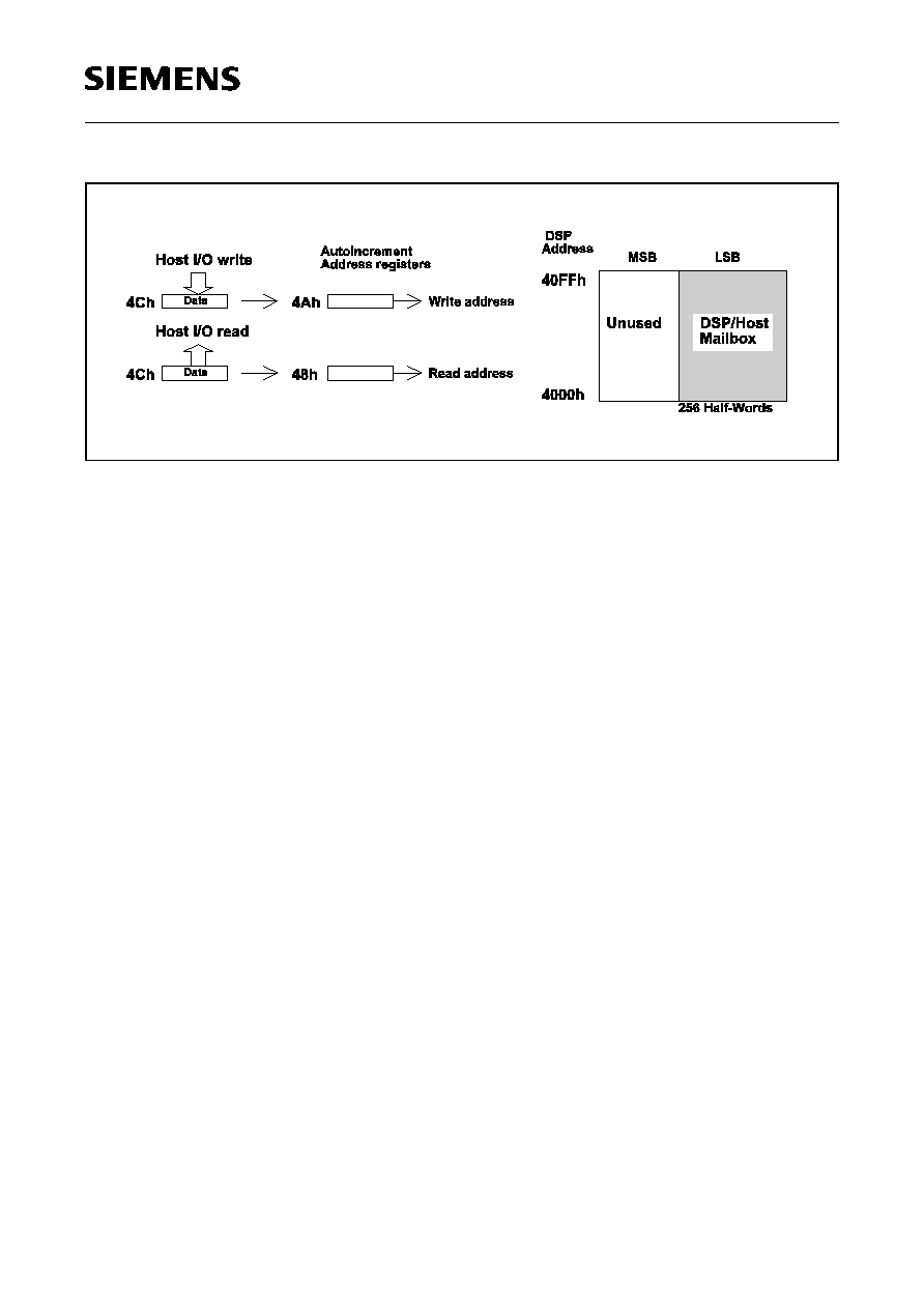
The Mailbox is seen from the host as an I/O device. Thus, to read or write a byte in the
Mailbox, the host accesses a single location (separate for read and for write Mailbox).
The address is given by an address register directly programmable by the host. This
address is autoincremented every time an access by the host to the Mailbox I/O address
is performed. Thus, for sequential, fast access, the Mailbox is seen as a 256-byte, full
duplex FIFO. For random accesses to the Mailbox the Host has to reprogram the
address register(s). This is summarized in Figure 18.
PSB 7230
Interfaces and Memory Organization
Semiconductor Group
45
Data Sheet 1998-07-01
Figure 18
I/O Access From the Host to the Mailbox (Summary)
Read
Host programs the desired start address (00
H
to FF
H
) into address register 48
H
.
Loop:
A read access from Host to 4C
H
gives the data from the current location in the read
Mailbox pointed to by the address register in 48
H
.
The address register is autoincremented.
Go to Loop.
Write
Host programs the desired start address (00
H
to FF
H
) into address register 4A
H
.
Loop:
A write access from Host to 4C
H
writes the data into the current location in the write
Mailbox pointed to by the address register in 4A
H
.
The address register is autoincremented.
Go to Loop.
(In the case of overflow, the address register 48
H
or 4A
H
wraps around to 00
H
.)
Software Handling of Communication via Mailbox
To indicate that data is ready to be read by the host/DSP, the DSP/host may use a
general purpose 8-bit interrupt register located in the Host/DSP Comm section of the
Directly Accessible Register Bank (DARB), associated with a 16-bit soft command and
status word in the same area. This protocol is implemented in software. The same
applies for indicating to the host/DSP that data has been read, in other words, the
memory in one direction is free. See Example below for using the Mailbox involving a
handshake protocol between the DSP and the Host.

PSB 7230
Interfaces and Memory Organization
Semiconductor Group
46
Data Sheet 1998-07-01
Simultaneous read/write is not prohibited by hardware, but a handshake mechanism (via
IND/INH software interrupt registers with optional Control Data) is implemented in
software.
Procedure from Host to DSP (example):
a) Host
Write Mailbox (1 to 256 bytes) if free (released by DSP)
Write word in Control register (60 - 61
H
) (e.g. number of bytes in Mailbox)
Write 8-bit vector in INH
Internally, this causes an INT1 interrupt to DSP, which recognizes a "soft interrupt"
(firmware)
DSP: Services INT1 and Acknowledges by Writing an 8-bit Vector in IND
Host
Read IND
Jump into routine pointed to by IND: "Mailbox release"
Write further data, etc.
3.4.1
DSP/Host Com Area with a Demultiplexed Host Interface
The DSP/host communication area contains the registers to support hardware and
software interrupts and special purpose registers that support communication between
the embedded DSP and the host. In demultiplexed mode, data are available on pins on
pins AD(0-7), whereas the address is supplied on pins A(0-3). This mode gives an
additional and more microprocessor-like way of accessing the DSP/Host Com Area. The
most important registers are accessible via 3 address pins only and by the use of an
additional pin (A3) it is possible to access the complete range of the DSP/Host Com
Area. The address mapping versus the multiplexed host interface is given in Table 12.

PSB 7230
Interfaces and Memory Organization
Semiconductor Group
47
Data Sheet 1998-07-01
Table 12
Address Mapping of Multiplexed/Demultiplexed Host Interface
Address
A0-3
Demultiplexed Mode
Data D0-7
Address
AD0-7
Multiplexed Mode
Data AD0-7
Host Write
Host Read
Host Write
Host Read
FF
H
- FE
H
reserved
reserved
FD
H
- FC
H
reserved
reserved
77
H
Acknowledge
INT MSB
76
H
Acknowledge
INT LSB
75
H
Interrupt INT
Mask MSB
Interrupt INT
Status MSB
74
H
Interrupt INT
Mask LSB
Interrupt INT
Status LSB
73
H
Acknowledge
INTR
71
H
Interrupt
INTR Mask
MSB
Interrupt
INTR Status
MSB
70
H
Interrupt
INTR Mask
LSB
Interrupt
INTR Status
LSB
6C
H
reserved reserved
6A
H
reserved reserved
61
H
Cntrl Host
DSP MSB
Cntrl DSP
Host MSB
60
H
Cntrl Host
DSP LSB
Cntrl DSP
Host LSB
0F
H
- 0E
H
reseved

PSB 7230
Interfaces and Memory Organization
Semiconductor Group
48
Data Sheet 1998-07-01
The shaded registers are mapped to the demultiplexed mode and can be accessed in
demultiplexed mode by using address pins A(0-2), i.e. addressing 00
H
to 07
H
. Using A3
gives an additional way of accessing the DSP/Host Communication area by 2 registers
only. The address register 08
H
is written with the target address (from the multiplexed
mode) and the data register 09
H
contains the corresponding value or can be written with
a new value for the target address.
The function of the registers 00h to 07
H
is the same as described in Chapter 3.3.2.1.
0D
H
- 0C
H
reserved
58
H
INDB (LSBit)
IND Interrupt
Status
50
H
INH Interrupt
Status
INHB (LSBit)
4C
H
Mailbox IO
write
Mailbox IO
read
09
H
Data register
Data register
4A
H
Mailbox write address
08
H
Address
register
Address
register
48
H
Mailbox read address
07
H
Interrupt INT
Mask MSB
Interrupt INT
Status MSB
06
H
Cntrl Host
DSP MSB
Cntrl DSP
Host MSB
47
H
Ext. Memory
Data high
05
H
Cntrl Host
DSP LSB
Cntrl DSP
Host LSB
46
H
Ext. Memory
Data low
04
H
INDB (LSBit)
IND Interrupt
Status
45
H
Ext. Memory
Addr high
03
H
INH Interrupt
Status
INHB (LSBit)
44
H
Ext. Memory
Addr low
02
H
Mailbox IO
write
Mailbox IO
read
01
H
Mailbox write address
41
H
Reg Data
Host
DSP
Reg Data
DSP
Host
00
H
Mailbox read address
40
H
Conf/Cont
Reg Address
RDY(LSBit)
Table 12
Address Mapping of Multiplexed/Demultiplexed Host Interface (cont'd)
Address
A0-3
Demultiplexed Mode
Data D0-7
Address
AD0-7
Multiplexed Mode
Data AD0-7

PSB 7230
Functional Blocks
Semiconductor Group
49
Data Sheet 1998-07-01
4
Functional Blocks
4.1
Oscillator and Baud Rate Generator
Clocking Modes
The clock generator including PLL generates the internal master clock derived from an
input clock (or crystal) on pins XTAL(1:2).
Because of integrated decoupling capacitors, DC components of the input frequency on
XTAL(1:2) are filtered out. Consequently, for a crystal input (nearly a sinusoid), an
internal clock of nearly 50% duty cycle results.
The different clock modes available in the PSB 7230 are as follows:
For the clock generation unit a separate supply voltage pin (
V
DDA
and
V
DDAP
)
and a
separate ground pin (
V
SSA
and
V
SSAP
)
are provided.
The block diagram of the clock circuitry is shown in Figure 19.
CM1 = 0
PLL is activated by firmware after reset. The internal clock circuitry
generates a frequency 4.5 times the input on XTAL(1,2). The internal
frequency required is 34.56 MHz and is obtained by providing a
frequency of 7.68 MHz on XTAL1 input.
CM1 = 1
PLL inactive. The internal frequency is directly input via XTAL(1,2).
When using a crystal, a 34.56 MHz crystal swinging at its basic
harmonic has to be connected to XTAL(1,2).

PSB 7230
Functional Blocks
Semiconductor Group
50
Data Sheet 1998-07-01
Figure 19
For a proper initialization the required total length of the RESET is 1 ms.
Note: After a hardware reset, the JADE firmware needs to initialize its internal memories
and interfaces. The time to do this is less than 10 ms. The user must take care to
access the JADE only after this initialization phase is completed, i.e. 10 ms after
the hardware reset.
Power-down
The actual chip internal clock ("DSP clock") is gated with the PU bit in the general
configuration/control register. Thus, when PU is set to `0' (either via the host or the DSP),
clock distribution is stopped and the DSP is disabled. In this mode the power
consumption is minimum (software power-down). Only an interrupt to the DSP (on INT0
or INT1) can restart the DSP clock.
The initial state of the PU bit is `1'.
The PU bit is used by the on-chip firmware for the firmware-controlled power-down (see
Chapter 6.1.3 for details).
IOM-2 Clocks
The IOM-2 clocking is either provided by separate timing inputs DCL and FSC,
independent of the other clocks, or maybe generated by the JADE itself (CGEN bit in
register 202B
H
). When generated by the JADE, only double rate clocking in TE mode
(DCL = 1.536 MHz, FSC = 8 kHz) is supported.
X TAL1
X TAL2
Os cilla to r
(Se pa rate
P o we r supply )
VD DA, VS S A
/2
F or C M1= 0 (input 7 , 6 8 MHz)
x 1 8
/2
34 . 56 MHz
C M1
0
M
U
X
P LL/Clo c k g e n era to r c i rc ui t
DIV
CKOBR
C LKO
1 9
1
INT0
INT1
OR
PU
1 => s e t P U
DSP
AND
D S P
clo ck
/25 6
/ T3
T3
14
T3 inte rrupt s ta tus
CKOEN
CM1
CKOEN
T3 EN
DIV
CM1
7 ,68 MHz
CKOS

PSB 7230
Functional Blocks
Semiconductor Group
51
Data Sheet 1998-07-01
When input, the DCL clock frequency is either equal to the data rate on DD/DU (if Clock
Rate Select bit CRS = 1) or twice the bit rate (if CRS = 0, default value after Reset). In
the last case it is ensured that the internal IOM-2 bit clock has a phase such that output
bits on DD/DU are correctly clocked out (see Figure 20).
Figure 20
CLKO
After reset the auxiliary clock output CLKO outputs a frequency of 7.68 MHz,
independent of the selection of CM1 bit. Alternatively, CLKO can be programmed (via
CKOS bit in register 2002
H
) to output a frequency obtained from the DSP clock via a
programmable baud rate generator (baud rate factor 1, 2, 3 ... 2
19
).
The wide range for the division factor for the CLKO output allows also for the possibility
to use it as a time marker (period on the order of 10 ms to synchronize another device
to the PSB 7230 time base).
When using the PLL (CM1 = 0), it is made sure that during reset phase CLKO delivers a
continuous 7.68 MHz clock. When using the non-PLL mode (CM1 = 1) CLKO goes low
while reset phase.

PSB 7230
Functional Blocks
Semiconductor Group
52
Data Sheet 1998-07-01
4.2
Audio and Data Reception/Transmission
The PSB 7230 supports a total of four independent serial I/O-channels:
≠ one receive and one transmit audio channel, and
≠ one receive and one transmit data channel (pertaining to the serial Data controller).
The four channels are transferred between the DSP and/or the Parallel Host Interface
and one of the serial interface lines: DD or DU (IOM-2), or SR or ST (Serial Audio
Interface SAI). The capacity of each channel is individually determined by programming
the time-slot length on the selected serial interface line.
Timing Generation
The selection of the line for each of the channels is performed via SLIN1,0 (00: DU; 01:
DD; 10: SR; 11: ST). The timing logic is driven by the bit clock and frame synchronization
signals corresponding to the selected line. These are:
The IOM-2 timing signals can be input or output of the PSB 7230, i.e. the circuit is a slave
or master with respect to the IOM-2 interface. The selection is done by the CGEN bit in
register 202Bh.
The timing on the SAI lines SR and ST is either input or output. In the case where the
timing is internally generated (i.e. the PSB 7230 functions as SAI master for SR and/or
ST), a schematic diagram of the generation logic is shown in Figure 21.
DCL(/2) and FSC
for DD and DU
SCLK and RFS
for SR
SCLK and TFS
for ST.

PSB 7230
Functional Blocks
Semiconductor Group
53
Data Sheet 1998-07-01
Figure 21
Timing Generation on SAI Lines - Framesync
For the frame sync signal RFS and/or TFS, two basic modes of operation are provided:
Case 1:
If control bit RCONT = 1, pulses on RFS are continuously and periodically generated if
ERFS (Enable RFS generation control bit in data controller register bank) is set to "1", of
one bit period length and spaced (PRD + 1)
◊
16 bits apart, where PRD = 0, 1, ..., 31.
Note: It suffices that the ERFS bits in the serial Data Controller register bank is set to
"
1
"
in order for pulses to be generated.
Case 2:
If RCONT = 0, a burst of REP + 1 pulses on RFS is generated, of one bit period duration
and spaced 16 bit periods apart when a start command is issued by setting the STR bit
to "1". REP takes the a value in the range 0 to 1,023.
Note: (It suffices that the STR command in the serial Data Controller register bank is
issued in order for the generation of pulses start.)
The same applies for TFS (control bits are ETFS and STX).
SCLK (in)
DSP clock
Div
PRSC
10
M
U
X
SCKIN
0
1
Baud-Rate
Generator
STR/ERFS
1
RCONT RPRD/RREP
1
10
RFS(in)
0
1
M
U
X
RFIN
RFS (out)
0
Baud-Rate
Generator
STX/ETFS
1
TCONT TPRD/TREP
1
10
TFS(in)
1
M
U
X
TFIN
TFS (out)
SCLK (out)

PSB 7230
Functional Blocks
Semiconductor Group
54
Data Sheet 1998-07-01
Figure 22
Timing Generation on SAI Lines - Continuous and Burst Mode
The uses of these modes are as follows:
Case 1:
When the timing is input, or when it is internally generated with TCONT = 1, the interface
can be used as a general Time-Division Multiplex highway with time-slots of
programmable lengths and locations for audio and data.
Case 2:
When the timing is output with TCONT = 0, the interface is typically used to transfer
messages or blocks of compressed or uncompressed audio or data, preceded by a
header of control information pertaining to the transferred data block and synchronous
to it. The blocks can be received and transmitted using the serial Data Controller. An
application of this mode of operation is the synchronous transfer of H.221/223 oriented
data between the PSB 7230 and an attached VCP Videocodec.
Audio Channel Transfer
As mentioned in Section 3, all the serial channels (1 receive audio, 1 transmit audio, and
one full-duplex transparent data channel) can be transferred between one of the serial
interfaces and the DSP or the host in a flexible manner.

PSB 7230
Functional Blocks
Semiconductor Group
55
Data Sheet 1998-07-01
The interface to each of the audio channels is a 32-bit wide shift register. In receive
direction, when the shift register is filled to a programmable level (up to 32 bits), the
whole 32-bit shift register is loaded into the receive channel read register set accessible
from the DSP and from the host. Simultaneously, a maskable interrupt status is set.
Similarly, in the transmit direction, transmit channel data is loaded from the write register
pertaining to that channel (either from DSP or host register, as selected via a control bit)
into the transmit shift register when a selectable number of bits have been shifted out.
The buffering of up to 32 bits reduces the reaction time of the DSP software.
As an alternative to this, the audio channel data can also be loaded from the shift register
to the DSP/host registers (receive direction) and from the DSP/host registers into the
shift register (transmit direction) at the occurrence of the frame sync pulse. In this case
the number of significant bits in the registers is determined by the time-slot length
programmed on the receive/transmit line. The DSP/host has 125
µ
s to read/write the
register while new data is assembled or the contents of the shift register are transmitted,
during the following frame (this option could be used for DSP software synchronized on
the 8 kHz time base).
The audio channel registers, each of length 2 words/4 bytes, are (see Section 3):
The relevant parameters for controlling the transfer of the audio channels are
(independent for each channel):
The maskable interrupt status bits for controlling the transfer are:
or optionally:
RC1
Receive channel 1
XC1
Transmit channel 1
EN
Enable channel
LMOD
Load Mode (either once per frame, or after LBIT bits have been received/
transmitted)
LBIT
Load Bits. Gives the number of bits (1 to 32) to be loaded, in multiples of
the physical time-slot length.
BFUL
Buffer full (RC1)
BEMP
Buffer empty (XC1)
FSC
Frame Sync interrupt (FSC)
RFS
Frame Sync interrupt (RFS)
TFS
Frame Sync interrupt (TFS)

PSB 7230
Functional Blocks
Semiconductor Group
56
Data Sheet 1998-07-01
In addition, the control bit HXA1 controls whether the audio transmit channel is loaded
into the shift register from the XC1 register accessible from the DSP (HXA = 0) or from
the host (HXA = 1).
The block diagrams for the receive and transmit audio channels are shown in Figure 23
and Figure 24.
Figure 23
Figure 24
*Caption to the Figures:
In receive direction, the input data is loaded from the shift register into DSP accessible
read registers and simultaneously into (physically separate) host accessible read
registers.
In the transmit direction, data is loaded into the shift register from the transmit channel
register accessible from the DSP (if HXA = 0) or the register accessible from the host (if
HXA = 1). The control bit HXA1 is provided for this purpose.

PSB 7230
Functional Blocks
Semiconductor Group
57
Data Sheet 1998-07-01
Serial Data Channel Transfer
The interface between the input of the serial data receiver and the DSP or host, and
between the output of the transmitter and DSP or host is in each case a 32-bit long shift
register.
Receiver in LMOD(1:0) = 01, 10, 11
In receive direction, when the shift register from the serial line is filled to a programmable
level (1, 2 or 4), the whole 32-bit shift register is loaded into the HRR1/2 read registers,
physically separate for DSP and host. In the same cycle the contents of the HRW1/2
write register accessible from the DSP (if HHR1/2 = 0) or host (HHR1/2 = 1) are loaded
to the HDLC receiver input. In the next cycle the data from HRR1/2 is as a default loaded
into HRW1/2 and a maskable interrupt status BFHR1/2 is generated to the DSP and
host. The interrupt status is generated to both DSP and host, independent of the setting
of HAH1/2. If the data in HRR1/2 is to be pre-processed, the HRW1/2 register can be
overwritten by the DSP or host before the next 1, 2 or 4 bytes (programmable) have been
shifted into the shift register.
After reset (RRES) when starting the receiver (RAC = 1), the reset status data of HRW
and HRR is ignored by the receiver, i.e. the contents of HRW1/2 and HRR1/2 are not
forwarded to the HDLC receiver, but only the data received from the line. The same
applies to the interrupts: A BFHR1/2 interrupt is only generated after the first 1, 2 or
4 bytes of line data are available in the HRR1/2 register. Due to this pipeline, a latency
occurs in the HDLC/transparent serial data reception, see section below.
The start of the reception can be in the same frame (w.r.t. the frame sync signal on the
chosen line) as the setting of RAC = 1 since the time-slot count logic works
independently of RAC.
In transparent mode (TMO = 1) the reception is only started at the beginning of the time-
slot (time-slot aligned). If RAC is set to `1' during the selected time-slot, the receiver waits
for the beginning of the time-slot in the next frame.
Receiver in LMOD(1:0) = 00
The same applies for LMOD = 00, except the pre-processing is not available. The data
from the bit-reversal unit is bypassed to the HDLC receiver. In addition, the loading of
HRR1/2, HRW1/2 and the generation of the interrupt BFHR1/2 is done like in the other
LMODs for observation of the data stream by the DSP or host only. Thus, the
LMOD = 00 is identical with LMOD = 01, except pre-processing is not available and the
receiver latency after reset is shortened, see section below.

PSB 7230
Functional Blocks
Semiconductor Group
58
Data Sheet 1998-07-01
Transmitter in LMOD(1:0) = 01, 10, 11
Similarly, in the transmit direction, after 1, 2 or 4 bytes (programmable) are shifted out of
the shift register, the contents of the HXW1/2 write register accessible from DSP
(if HHX1/2 = 0) or host (if HHX1/2 = 1) are loaded into the transmitter shift register. In the
same cycle 1, 2 or 4 bytes are loaded from the HDLC transmitter output into the HXR1/
2 read register, physically separate for DSP and host. In the next cycle the data from
HXR1/2 is as a default loaded into HXW1/2 and a maskable interrupt status is generated
to the DSP and host. The interrupt status is generated to both DSP and host,
independent of the setting of HAH1/2. If the data in HXR1/2 is to be post-processed, the
HXW1/2 register can be overwritten by the DSP or host before the next 1, 2 or 4 bytes
(programmable) have been shifted out of the shift register.
After reset (XRES), the reset status data of HXR1/2 and HXW1/2 is ignored by the
transmitter, i.e. the contents of HXR1/2 and HXW1/2 are not transmitted to the line, but
only the data from the HDLC transmitter. In the first cycle after the transmitter has been
activated (XAC = 1), the data from the HDLC transmitter is immediately passed to the
HXR1/2 register for post-processing. The line-transmission is not yet started! In the first
cycle after the DSP or host (programmable via HHX1/2) has written the HXW1/2 register
with the post-processed value, this value is passed through the bit-reversal unit into the
shift register and the transmission is started as soon as the next beginning of the
selected time-slot is detected.
The start of the transmission can be in the same frame (w.r.t. the frame sync signal on
the chosen line) as the setting of XAC = 1 and/or the writing to the HXW1/2 register since
the time-slot logic works independently of XAC.
In transparent mode (TMO = 1) the transmission is only started at the beginning of the
time-slot (time-slot aligned). If the first write to HXW1/2 happens during the selected
time-slot, the transmitter waits for the beginning of the time-slot in the next frame.
Transmitter in LMOD(1:0) = 00
The same applies for LMOD = 00, except the post-processing is not available. The data
from the HDLC transmitter is after XAC = 1 directly passed through the bit-reversal unit
into the shift register. In addition, the loading of HXR1/2, HXW1/2 and the generation of
the interrupt is done like in the other LMODs for observation of the data stream by the
DSP or host only. Thus, the LMOD = 00 is identical with LMOD = 01, except
post-processing is not available and the transmitter latency after reset is shortened, see
section below. The transmission is in this case started by the setting of XAC = 1. No write
to HXW1/2 is necessary.
The start of the transmission can be in the same frame (w.r.t. the frame sync signal on
the chosen line) as the setting of XAC = 1 since the time-slot logic works independently
of XAC.

PSB 7230
Functional Blocks
Semiconductor Group
59
Data Sheet 1998-07-01
In transparent mode (TMO = 1) the transmission is only started at the beginning of the
time-slot (time-slot aligned). If XAC is set to `1' during the selected time-slot, the
transmitter waits for the beginning of the time-slot in the next frame.
The serial data channel registers, each of length 2 words/4bytes, are (Section 3):
The relevant parameters for controlling the transfer of the serial data channels are:
The access right to the receiver and transmitter input/output from the DSP or the host
(determined bits HHR1 and HHX1) is independent of who is allowed to service the data
controller (determined by bits HAH1).
The maskable interrupt status bits for controlling the transfer are:
The block diagrams for the receive and transmit data Controller channel are shown in
Figure 25 and Figure 26.
HRR1
Data Receive Read 1
HRW1
Data Receive Write 1
HXR1
Data Transmit Read 1
HXW1
Data Transmit Write 1
LMOD(1:0)
Load Mode (access byte by byte without delay, or access in 1, 2 or 4 byte
units with a corresponding serial data delay)
HHR
Access to serial data receiver input from DSP (HHR = 0) or from host
(HHR = 1)
HHX
Access to serial data output shift register from DSP (HHX = 0) or from host
(HHX = 1).
BFHR
Buffer full for data receiver (new data can be read from HRR and written
into HRW)
BFHX
Buffer full for data transmitter (new data can be read from HXR and written
into HXW)

PSB 7230
Functional Blocks
Semiconductor Group
60
Data Sheet 1998-07-01
Figure 25
Caption to the Figure
The data from the shift register is loaded into DSP accessible read registers and
simultaneously into (physically separate) host accessible read registers. Data to the
receiver is loaded from the transmit channel register accessible from the DSP (if
HHR = 0) or the register accessible from the host (if HHR = 1). The control bit HHR1 is
provided for this purpose.

PSB 7230
Functional Blocks
Semiconductor Group
61
Data Sheet 1998-07-01
Figure 26
Caption to the Figure
The data from the data transmitter is loaded into DSP accessible read registers and
simultaneously into (physically separate) host accessible read registers. Data is loaded
into the shift register from the transmit channel register accessible from the DSP (if
HHX = 0) or the register accessible from the host (if HHX = 1). The control bit HHX1 is
provided for this purpose.
The access right to the receiver and transmitter input/output from the DSP or the host
(determined bit HHR1 and HHX1) is independent of who is allowed to service the data
controller (determined by bits HAH1).
Note on Time-Slots of Data Communication Controller
If a time-slot is still active (either in receive or transmit direction) when a new frame sync
pulse is detected, the programmed length of the time-slot is not reduced but the time-slot
remains active until its end. However, the time-slot count logic for the new frame starts
immediately at the detection of the new frame sync pulse. A new time-slot can start
immediately after the currently active time-slot has been closed, thus permitting a
permanent reception or transmission ("time-slot length" = "distance between two
consecutive frame sync's").
The case where "time-slot length" > "distance between two consecutive frame sync's"
should not occur.

PSB 7230
Functional Blocks
Semiconductor Group
62
Data Sheet 1998-07-01
Note on Latency of Serial Data
When the data receiver is enabled (via bit RAC), the data receiver is clocked with the
serial interface clock even outside the selected time-slot. However, the logic at the input
of the data receiver is only clocked with the serial clock during the selected time-slot.
Consequently, N bits are loaded into HRR register from the serial line after N clock edges
inside the selected time-slot (N is equal to 8, 16 or 32 depending on LMOD). Similarly,
data from HRW register is loaded into data receiver only after a certain number of clock
edges inside the selected time-slot have occurred. The latency (delay) of received data
from the input pin to the data FIFO is given in the following as a function of LMOD (C
TS
means the number of clock edges inside the active time-slot, C means the number of
clock edges independent of the active time-slot):
Similarly, latencies apply in the case of the data from the output of the data transmitter
FIFOs to the serial output pin. Those are different for the first 1, 2 or 4 bytes ("start") and
the following bytes ("stationary"):
t
: Delay between BFHX1 interrupt status and write to HXW1 register by DSP or host
(programmable via HHX1).
Table 13
Receiver Delays
Start & Stationary
LMOD = 00
8 C
TS
+ 9 C
LMOD = 01
16 C
TS
+ 9 C
LMOD = 10
32 C
TS
+ 17 C
LMOD = 11
64 C
TS
+ 33 C
Table 14
Transmitter Delays
Start
Stationary
LMOD = 00
10 C
10 C + 8 C
TS
LMOD = 01
11 C +
t
10 C + 16 C
TS
LMOD = 10
19 C +
t
18 C + 32 C
TS
LMOD = 11
35 C +
t
34 C + 64 C
TS

PSB 7230
Functional Blocks
Semiconductor Group
63
Data Sheet 1998-07-01
During reception/transmission the delay is dynamically increased by the number of zero
insertions in the path between the line and the data receiver/transmitter. Thus, the
numbers in the table refer to the beginning and the end of the frame and any state inside
a frame when no zero insertions are in the pipeline.
The receiver latencies have to be taken into account in systems where the serial clock
is not continuous but is immediately disabled after the last serial data bit has been
received.
The transmitter latencies have to be taken into account in systems where the transmitter
shall start transmitting accurately in one special frame (w.r.t. the line frame sync signal),
e.g. when the transmission has to be started in the first time-slot of a frame-sync burst.

PSB 7230
Functional Blocks
Semiconductor Group
64
Data Sheet 1998-07-01
4.3
Serial Data Controller
The internal serial data controller of the PSB 7230 can be independently serviced
≠ either via the Parallel Host Interface
≠ or by the DSP (SPCF).
Important Notes:
1. From the point of view of the end user/system manufacturer, only the servicing of the
data controller via the host is of relevance, since the servicing via the DSP is done by
on-chip firmware invisible to the end user.
2. If the packet oriented protocol on the Serial Audio Interface used in videophone
applications with the VCP (from 8x8, Inc.) videocodec is needed, the data controller is
serviced by the on-chip firmware, in other words, it cannot be accessed by the host.
Only in protocols (see Section 6.2) with the compressed data stream via host
interface the serial data controller is available for host usage.
The servicing of the data controller via the host and via the embedded DSP are exclusive
of each other. The access to the register banks of the data controller is determined by
the "Data Controller Access from Host" bit HAH1:
≠ When HAH1 is "0", the SPCF is allowed to access the data register bank, and the Host
interface bus is disconnected from the data controller;
≠ When HAH1 is "1", the Host is allowed to access the data register bank, and the SPC
data bus is disconnected from the data controller.
The address space of the data controllers for the Host interface bus and for the SPC data
bus is shown in Figure 27 (see also Section 5): Data Controller Register Description):
Figure 27

PSB 7230
Functional Blocks
Semiconductor Group
65
Data Sheet 1998-07-01
The received data is stored in the receive FIFO so that byte alignment in the FIFO
corresponds to byte alignment in the serial time-slot (if the length of the time-slot is a
multiple of 8 bits). Similarly, in transmit direction the byte alignment in the FIFO
corresponds to the time slot boundaries in the transmit time-slot, if its length is a multiple
of 8 bits. When the transmit FIFO is empty, idle ("1") is transmitted during the active time-
slot. Outside the selected time-slot, the output line is in "high impedance" state.
Details on the Operation of the Serial Data Receiver
The data receive FIFO size is 2
◊
32 bytes. One half of the FIFO is connected to the
receiver shift register while the second half is accessible from the controlling software.
The status bits pertaining to the data receiver are:
The data receiver is controlled by the following bits:
Details on the Operation of the Serial Data Transmitter
The transmit FIFO size is 2
◊
32-bytes. One half is connected with the transmit shift
register while the other half is accessible via the controlling software.
The interrupt status bits pertaining to the data transmitter are:
RPF
Receive Pool Full
32 bytes of a frame have arrived in the receive FIFO. The frame has not yet
been completely received.
RFO
Signifies that data has been lost because no room was available in RFIFO.
RAC
Receiver Active
When RAC is set to "1", storage of bytes in the receive FIFO starts time-slot
aligned (if the receive time-slot length is a multiple of 8 bits).
RMC
Receive Message Complete
Acknowledges a previous RPF status. Frees the FIFO pool for the next
received frame or part of a frame.
RRES
Receiver Reset
Resets the data receiver, which goes into an idle state (RAC cleared), clears
the receive FIFO.
XPR
Transmit Pool Ready
One data block may be entered into the transmit FIFO.
ALLS
All Sent.
When "1", indicates that the last bit has been transmitted and that the XFIFO
is empty.

PSB 7230
Functional Blocks
Semiconductor Group
66
Data Sheet 1998-07-01
The following status bits are provided:
The data transmitter is controlled by the following bits:
After up to 32 bytes have been written to the FIFO, transmission is started by issuing the
XF command. The data controller requests another data block by an XPR interrupt
status if there are no more than 32 bytes in the FIFO. To this the software responds by
writing another pool of data and issuing a transmit command XF for that data. If
transmission of earlier data (or of a previous frame) is still underway when a new
transmission command XF is issued, software access to the FIFO is blocked until the
first transmission is completed.
If the transmit FIFO runs out of data, the host will be advised by a Transmit Data Unterrun
(XDU) interrupt status.
XDOV
Transmit Data Overflow
Indicates that more than 32 bytes have been written into the transmit FIFO
XAC
Transmitter Active
In transparent mode, when XAC is set to "1", transmission of bytes from the
transmit FIFO starts time-slot aligned (if the transmit time-slot length is a
multiple of 8 bits).
XF
Transmit Frame
Initiates transmission of an entire frame, or part of one (up to 32 bytes).
XRES
Transmitter Reset.
Resets the data transmitter, clears the transmit FIFO and generates an XPR
status after the command has been completed.
XNEW
Transmitter Restart
Resets the transmitter state machine without any loss of data (i.e. FIFO
data). The transmission of the current frame can be restarted with the first
bit of the start flag.

PSB 7230
Functional Blocks
Semiconductor Group
67
Data Sheet 1998-07-01
4.4
IOM-2 Functions
The IOM-2 functions supported by the PSB 7230 are:
≠ Layer 1 functions in terms of the frame structure supporting any number n of 4-byte
multiplexes (n = 1, ..., 16), the number is implicitly determined by the DCL clock (see
Section 2)
≠ One Monitor channel of programmable location
≠ Two C/I channels.
See Figure 28.
Monitor Channel
Figure 28
Parameters:
C/I Channels (2 Independent Channels)
Figure 29
SLIN = 0:
Monitor transmit data on DU, receive data on DD
SLIN = 1:
Monitor transmit data on DD, receive data on DU
CH(0:3):
Monitor channel in 3rd byte of multiplex 0, ..., 15 (common to receive
and transmit channel) (CH(0:3) = 0001 in the example)

PSB 7230
Functional Blocks
Semiconductor Group
68
Data Sheet 1998-07-01
Parameters:
4.4.1
Monitor Channel Protocol
Use of Monitor Channel
In the case where a
local host
is present, the Monitor channel may be used e.g. for data
exchange between the local host and another controller attached to the IOM-2 bus. For
this purpose the basic Monitor channel protocol as explained in this section is sufficient.
Note: The Monitor channel protocol is not implemented on-chip on the PSB 7230. The
Monitor channel protocol has to be implemented via the host: this allows the
implementation of data exchange with a remotely located controller.
General Description of Monitor Channel Protocol
The Monitor channel consists of 8 bits for the Monitor Data channel (MON) and 2 bits for
the flow control (MX and MR). The transmitter controls the Monitor Data channel and the
MX bit on one line while evaluating the condition of the MR bit on the other line. The
receiver evaluates the MX bit of one line and latches its Monitor Data value. It controls
the MR bit of the other line. The Monitor channel protocol is shown in the figure below.
The hardware performs reception and transmission of Monitor channel messages
(packets) byte by byte under software control.
The received and transmitted Monitor channel bytes are stored in the Monitor Data
Transmit (MONX) register and Monitor Data Receive (MONR) register, respectively.
The software controls the monitor channel via two control bits in the Monitor channel
Control Register:
SLIN = 0:
C/I channel transmit data on DU, receive data on DD
SLIN = 1:
C/I channel transmit data on DD, receive data on DU
CH(0:3)
C/I channel in 4th byte of multiplex 0, ..., 15, common for receive and
transmit channel (CH(0:3) = 0001 in the example)
CIL:
C/I channel length is 4 bits (0) or 6 bits (1)
DLL:
Double last look yes (1) or no (0)
MRE
Monitor channel Receiver Enable
MRC
MR bit Control
MXC
Monitor channel Transmitter Control.

PSB 7230
Functional Blocks
Semiconductor Group
69
Data Sheet 1998-07-01
The Monitor channel status is reported to the software via four bits in the Monitor channel
Status register:
Inactivity
The transmitter indicates its inactivity with the idle state of the MX bit (1) and by
transmitting the value FF
H
(or high impedance) in the Monitor Data channel. The receiver
responds to this inactivity via the idle (1) condition of the MR output bit.
Monitor Packet Transfer
The message transfer starts when the transmitter transmits the value of the first byte of
the Monitor Data channel and sets the MX bit to its active state (0). The MX bit remains
active until the receiver acknowledges the data or the transmitter software aborts the
transmission. The receiver recognizes the change of the MX bit to the active state and
latches the contents of the Monitor Data channel. Since the Monitor channel address is
always transmitted as the first byte of a message, all receiving devices compare (per
hardware or software) the first value with their own address. If a device recognizes its
address it acknowledges the data by changing its MR bit to the active state (0).
The transmitter recognizes this change and can now transmit the next byte of the
message. This is done by transmitting the value in the Monitor Data channel and setting
the MX bit to the inactive, idle (1) state for one frame and then changing it back to the
active (0) state. The receiver recognizes the transition of MX from the inactive to the
active state and latches the contents of the Monitor Data channel.
The receiver acknowledges the data transfer by setting the MR bit to the inactive (1) state
for one frame and then back to the active (0) state. This procedure is repeated until all
the data is transferred. Once the receiver has acknowledged the last value the
transmitter switches its MX bit and the Monitor channel into the idle (1) state. The
receiver recognizes this idle state after it has received two consecutive frames with an
idle MX bit and will then set its own MR bit in the idle (1) state.
The transmitter recognizes the change of the MR bit and indicates the idle condition after
the second frame. If the receiver wants to abort a transmission, then it will set its MR bit
into an idle (1) condition. The transmitter recognizes the abort condition after the second
frame with an idle MR bit and switches its MX bit and the Monitor Data channel to idle.
MDR
Monitor channel Data Received
MER
Monitor channel End of Reception
MDA
Monitor channel Data Acknowledged
MEA
Monitor End of Acknowledgement
MAB
Monitor channel Abort.

PSB 7230
Functional Blocks
Semiconductor Group
70
Data Sheet 1998-07-01
Figure 30
Note: For simplification of the diagram the states of MX and MR are shown as
"
0
"
or
"
1
"
during the entire 125
µ
s frame without regard to the bit positions they actually
occupy.
Software Handling of Monitor Channel Transmission
The idle state of the transmitter is maintained when the MXC (Monitor channel Transmit
Control) bit is 0. In order to transmit the first byte, its value is written into the MONX
(Monitor channel Transmit) Register. After the MXC bit is set to 1, the Monitor channel
hardware sends the byte from MONX and controls the MX bit accordingly (MX:1
0).
When the hardware detects the acknowledgment from the other end (received
MR bit = 0), it will set the MDA (Monitor Data Acknowledged) bit. When this is detected
by the software, it writes the next byte in MONX register. This byte is sent and the MX
bit controlled accordingly. The acknowledgment by the other end is again indicated by
the MDA status bit. This procedure is repeated until all the data is transmitted. After the
last MDA status the software sets the MXC bit back to 0 and the transmit channel
including the MX bit returns to the idle state.
If an abort request from the receiving end is detected by the hardware, the MAB (Monitor
channel Abort) status bit is set.
In the PSB 7230 the Monitor channel transmitter implements the so-called Maximum
speed option of this protocol, whereby the acknowledgment of every byte (except the
first) by the receiving end is anticipated. This means that an MDA interrupt status is
generated as soon as the received MR bit is detected to go from 0 to 1. Transmission of
the next byte is started as soon as the software has reacted to this interrupt. Thus a
maximum transfer speed of 32 Kbit/s can be obtained.

PSB 7230
Functional Blocks
Semiconductor Group
71
Data Sheet 1998-07-01
Each data byte is transmitted at least twice (only twice if the receiver is fast enough so
that the transmitter works at maximum speed), namely once when MX is 1, and once
when MX is 0 in the next frame. The only exception is the first byte, which is transmitted
in three consecutive frames (where MX = 1, 0, 0, respectively).
In order for the transmitter to recognize that the receiver has correctly acknowledged the
last byte, the interrupt status MEA is set after the received MR bit is received at 1 in two
consecutive frames (interrupt status different from MAB). The condition for generating
an MEA interrupt status is the recognition of a MR = 0, 1, 1 sequence when MXC = 0.
Figure 31
Figure 31 shows the general case, Figure 32 the maximum speed case.
Software Handling of Monitor Channel Reception
The receiver of the Monitor channel is controlled via the MRE bit. As long as the MRE bit
is zero, no evaluation of the received MX bit is done. If the MRE bit is set to 1, then the
Monitor channel hardware waits for a start of a Monitor packet. When the start of a
packet is recognized with a Monitor byte matching monitor receive address,
acknowledgement can be enabled by the software by setting the MR Control bit MRC

PSB 7230
Functional Blocks
Semiconductor Group
72
Data Sheet 1998-07-01
to 1. The hardware performs acknowledgement by setting the transmitted MR bit to 0.
Upon the reception of the next byte the hardware sets the MDR status bit. When the
Monitor byte is read from the MONR register, this byte is acknowledged via transmit
MR = 0. Every new byte is similarly indicated by the MDR status, and acknowledged
after a read of the MONR register. If the hardware recognizes the end of a packet, it
indicates this via the MER status (MRE = 1).
The receiver of the PSB 7230 does not perform a double-last-look check on the received
data (i.e. compare the data received while MX = 0 with the data in the previous frame
with MX = 1).
When MRC = 0, it is made sure that the receiver only receives the first byte of a packet
and does not latch any further bytes in MONR until the beginning of the next packet.
Thus the conditions for latching the first byte of a packet is:
(MRE = 1) & (MX = 0 after having been 1 in at least two consecutive frames).
Any further bytes are latched into MONR only if:
(MRE
◊
MRC = 1) & (previously received byte has been read from MONR register) &
(MX = 0).
Figure 32

PSB 7230
Functional Blocks
Semiconductor Group
73
Data Sheet 1998-07-01
Figure 33
Monitor Channel Data Transfer
A hardware model of the Monitor channel is shown below.
Figure 34
*) MRC has to be "1" and MONR has to be read before any new value from the same
packet is loaded into MONR. Thus, while MRC = 0, only the first byte of a packet is
loaded into MONR.

PSB 7230
Functional Blocks
Semiconductor Group
74
Data Sheet 1998-07-01
4.4.2
C/I Channel
The two C/I channels are controlled via the C/I Transmit (CIX) and C/I Receive (CIR)
registers, the C/I channel Enable (CIEN) and the C/I Change (CIC) interrupt status bit.
In addition, an Awake (AWK) control bit is provided. When this bit is set to "1", the output
line is unconditionally "low" until AWK is set to "0" again. This bit is used in ISDN terminal
applications to "wake up" the IOM-2 interface, i.e. to require clocking to be generated on
DCL and FSC by an upstream circuit - typically an ISDN S-Bus Access Controller
ISAC-S.
When the AWK bit is set to "0", the output line is released only after the next FSC pulse
has been detected, to avoid sending an invalid code in the outgoing C/I channel. C/I data
reception and processing begins after setting CIEN to 1. It is made sure that no invalid
code is sent or receiced. AWK overrides any data normally transmitted during the C/I
time-slot even if CIEN = 1. When CIEN (synchronized with FSC) is "0" and AWK
(synchronized with FSC) is "0", the outgoing C/I channel is permanently in
high-impedance state.
The block diagram of the C/I channel handler is shown below.
In the receive direction, a change is recognized either using Double Last Look (DLL = 1)
or not (DLL = 0).
Without Double Last Look
A change in received C/I channel is recognized after a new value is recognized once.
The new value is loaded into CIR for the DSP to read, and a CIC interrupt status is
generated.
If further changes in receive C/I code take place before a previous changed value in CIR
has been read, the changed values are not loaded in CIR.
When the first changed value is read by the DSP, the latest changed value is loaded in
CIR and a CIC interrupt status is generated anew. Any possible changes that occurred
between the first and the latest are thus lost.

PSB 7230
Functional Blocks
Semiconductor Group
75
Data Sheet 1998-07-01
With Double Last Look
A change in received C/I is recognized after a new value is detected in two consecutive
frames.
This is shown in Figure 35.
Figure 35
Algorithm:
"Current" is compared to "Previous":
≠ If they are not equal, "Current" is loaded into "Previous", and a new comparison is
performed in the next frame. No further actions are taken.
≠ If they are equal, the new value takes the place of "Confirmed". "Confirmed" is
compared to "Old Confirmed":
If they are equal, no actions are taken.
If they are not equal, "Confirmed" is copied to "Old Confirmed".
If CIR register has been read, "Old Confirmed" is compared to CIR:
≠ If they are equal, no actions are taken.
≠ If they are not equal, "Old Confirmed" is copied to CIR and a CIC interrupt status is
generated.

PSB 7230
Functional Blocks
Semiconductor Group
76
Data Sheet 1998-07-01
C/I Channel Data Transfer
The block diagram of the C/I channel handler is shown below.
Figure 36
*) Read of the old changed value is the condition of loading of a new changed value.
Thus, when several changes occur before the first changed value has been read, only
the first and the last change are available.
FSC
DD
DCL(/2)
Time-slot
Count
Logic
CIL CICH
1
4
Shift Register
Clock
6 bits
SLIN
1
M
U
X
1
0
DU
DSP or
Host
C/I channels 1,2:
DU
SLIN
1
M
U
X 1
0
DD
CIEN*Strobe+AWK
Shift Register
6 bits
CIX
6
6
Compare
logic
Load
CIR
Read
*)
DLL
Previous
Current
Load
CIC int status
M
U
X
0
1
0
AWK
Strobe
CIEN
1
DSP or
Host

PSB 7230
Functional Blocks
Semiconductor Group
77
Data Sheet 1998-07-01
4.5
Programming Indirectly Accessible Registers
Registers in the memory mapped (DSP X-data RAM) area from 2000
H
upwards are read
and written:
≠ via the Parallel Host Interface by using two registers (Conf/Cont Reg Address Register
at address 40
H
/3040
H
and Conf/Control Reg Data Register at address 41
H
/3041
H
)
4.5.1
Programming via Parallel Host Interface
(see also Section 3.3.2)
For writing a Configuration/Control register (addresses 2000
H
- 203F
H
), the host writes
in the Data register the data byte to be written and in the Address register the write
command:
where A(5:0) gives the offset of the register to be written. This causes an RACC
(Register Access) interrupt status to the DSP. The DSP software transfers the Data byte
to the requested address 2000
H
+ A(5:0) and writes the RDY bit (least significant bit of
address 40
H
/3040
H
) to "1" again (which was set to "0" by hardware at the time of writing
of the Address register). By sensing the state of bit RDY the host is able to start a new
access to Address and Data registers when the DSP is ready.
For reading a Configuration/Control register (addresses 2000
H
- 203F
H
), the host writes
in the Address register the read command:
where A(5:0) gives the offset of the register to be read. This causes a RACC (Register
Access) interrupt status to the DSP. The DSP software transfers the contents of the
requested address 2000
H
+ A(5:0) into the Data register and writes the RDY bit to "1".
Bit 7
Bit 0
0
0
A5
A4
A3
A2
A1
A0
Bit 7
Bit 0
1
0
A5
A4
A3
A2
A1
A0

PSB 7230
Register Description
Semiconductor Group
78
Data Sheet 1998-07-01
5
Register Description
5.1
Interrupt Structure
As explained in Section 3, the interrupt statuses are grouped on two interrupt lines, "high
priority" and "low priority" interrupts, respectively. They are:
High Priority Interrupts (INTR)
FSC, RFS, TFS
BFUL1, BEMP1, BFHR1, BFHX1
Lower Priority Interrupts (INT):
SAIN
SDATA
DINT
GPI
MDR, MER, MDA, MEA, MAB, CIC1, CIC2
Corresponding interrupt status register exist for the internal DSP.
The interrupt status registers are physically separate for the Host and for the DSP. Thus,
when an interrupt status is generated, the interrupt status bit is set in both registers.
The interrupt status disappears from the interrupt status register when the cause of the
interrupt status is removed by the software, or the interrupt is explicitly acknowledged.
Whenever possible, an interrupt status is made to disappear when the cause of that
interrupt status is removed (example: in/out audio data channel interrupts), in order to
spare the explicit writing of an acknowledge register address. In other cases the interrupt
statuses are explicitely acknowledged by writing a "1" in a virtual acknowledge register.
The interrupt status bits have individual mask bits which have no influence on the setting
of the interrupt status bits, but only on the generation of the interrupt on the interrupt line.
When the mask bit is 0, the generation of the interrupt for the corresponding interrupt
status on line INTR or INT is prevented.

PSB 7230
Register Description
Semiconductor Group
79
Data Sheet 1998-07-01
5.2
Interrupt Status Registers
Register Map for Host Interrupts
Host Interrupt Status for INTR:
Interrupt Mask Registers:
A "0" in a bit position masks the corresponding interrupt (default value, i.e. after Reset).
The mask bit affects only the generation of the interrupt, but not the interrupt status bit
from being set.
Bit 7
Bit 0
71
H
FSC
RFS
TFS
Bit 7
Bit 0
70
H
BFUL1
0
BEMP1
0
BFHR1
BFHX1
0
0
FSC
FSC detected
RFS
RFS detected
TFS
TFS detected
BFUL1
Receive channel sample of programmable length (1 ... 32 bits) available in
RC1
BEMP1
Transmit channel sample of programmable length (1 ... 32 bits) can be
written in XC1
BFHR1
Data receiver shift register can be read and/or written (1, 2 or 4 bytes) in HR1
BFHX1
Data transmitter shift register can be read and/or written (1, 2 or 4 bytes) in
HX1
Bit 7
Bit 0
71
H
FSC
RFS
TFS
Bit 7
Bit 0
70
H
BFUL1
BEMP1
BFHR1
BFHX1

PSB 7230
Register Description
Semiconductor Group
80
Data Sheet 1998-07-01
Acknowledge Register:
The interrupt status bit is reset when the host writes a "1" in the corresponding bit
position.
The other interrupt status bits are reset when the input/output registers are read or
written:
Host Interrupt for INT:
Bit 7
Bit 0
73
H
FSC
RFS
TFS
BFUL1
Reset when RC1 (address 00
H
) is read
BEMP1
Reset when XC1 (any of 00-03
H
) is written
BFHR1
Reset when HRR1 (any of 10-13
H
) is read
BFHX1
Reset when HXR1 (any of 14-17
H
) is read
Bit 7
Bit 0
75
H
0
0
0
SAIN
DINT
SDATA
0
Bit 7
Bit 0
74
H
MDR
MER
MDA
MEA
MAB
GPI
CIC1
CIC2
SAIN
Serial Audio Input Interrupt (from SIO line)
DINT
Software interrupt from DSP
SDATA
Interrupt from serial data Controller
MDR
Monitor Channel Data Received
MER
Monitor Channel End of Reception
MDA
Monitor Channel Data Acknowledged
MEA
Monitor End of Acknowledgment
MAB
Monitor Channel Abort Request
GPI
General Purpose Interrupt occured
CIC1
C/I Channel 1 Change
CIC2
C/I Channel 2 Change.

PSB 7230
Register Description
Semiconductor Group
81
Data Sheet 1998-07-01
Interrupt Status Mask Register:
A "0" in a bit position masks the corresponding interrupt (default value, i.e. after Reset).
The mask bit affects only the generation of the interrupt, but not the interrupt status bit
from being set. Undocumented mask bits must be always set to "0".
Acknowledge Register:
The interrupt status bit is reset when the host writes a "1" in the corresponding bit
position. The other interrupts are acknowledged as follows:
Note: Since no direct access to the MONR, CIR1, CIR2 and GP Int Status registers for
the host is allowed (these registers are in the Configuration and Control Register
area 2000
H
upwards), they are read using the procedure via Address and Data
registers as decribed in Section 2 ≠ in principle giving the host the possibility to
handle the Monitor and C/I channels via the DSP.
Bit 7
Bit 0
75
H
SAIN
DINT
SDATA
Bit 7
Bit 0
74
H
MDR
MER
MDA
MEA
MAB
GPI
CIC1
CIC2
Bit 7
Bit 0
77
H
SAIN
Bit 7
Bit 0
76
H
MER
MDA
MEA
MAB
DINT
Reset when IND Int. Status register is read
SDATA
Reset when serial data Controller interrupt register is read
MDR
Reset when MONR register is read
GPI
Reset when GP Int Status register is read
CIC1
Reset when CIR1 register is read
CIC2
Reset when CIR2 register is read.

PSB 7230
Register Description
Semiconductor Group
82
Data Sheet 1998-07-01
5.3
Indirectly Accessible Configuration and Control Registers
Table 15
Summary
Addr
Register
Name
Bit 7
Bit 6
Bit 5
Bit 4
Bit 3
Bit 2
Bit 1
Bit 0
2000
H
Chip
Version Nr
≠
≠
VN5
VN4
VN3
VN2
VN1
VN0
2001
H
External
Memory
LDMEM
CAEN
≠
DACC
NRW3
NRW2
NRW1
NRW0
2002
H
General
Config
PU
CRS
CKOEN
CKOS
ODS
CKOBR18 CKOBR17 CKOBR16
2003
H
CLKO Baud
Rate2
CKOBR15 CKOBR14 CKOBR13 CKOBR12 CKOBR11 CKOBR10 CKOBR9
CKOBR8
2004
H
CLKO
Baud Rate1
CKOBR7
CKOBR6
CKOBR5
CKOBR4
CKOBR3
CKOBR2
CKOBR1
CKOBR0
2005
H
SAI Mode
SODS
SPS
DSE
≠
≠
SCKIN
PRSC9
PRSC8
2006
H
SCLK
Baud Rate
PRSC7
PRSC6
PRSC5
PRSC4
PRSC3
PRSC2
PRSC1
PRSC0
2007
H
RFS Mode
RFIN
RCONT
RFE
RFSEL
RFPS
≠
RREP9
RREP8
2008
H
RFS Per/
Rep Rate
RREP7
RREP6
RREP5
RPRD4/
RREP4
RPRD3/
RREP3
RPRD2/
RREP2
RPRD1/
RREP1
RPRD0/
RREP0
2009
H
TFS Mode
TFIN
TCONT
TFE
TFSEL
TFPS
≠
TREP9
TREP8
200A
H
TFS Per/
Rep Rate
TREP7
TREP6
TREP5
TPRD4/
TREP4
TPRD3/
TREP3
TPRD2/
TREP2
TPRD1/
TREP1
TPRD0/
TREP0
200B
H
SIO Config
≠
≠
≠
≠
≠
SAIO
SOUT
SINTC
200C
H
≠
0
≠
0
0
0
0
0
0
200D
H
≠
0
0
0
0
0
0
0
0
200E
H
≠
0
0
0
0
0
0
0
200F
H
≠
0
0
0
0
0
0
0
0
2010
H
Data Cntr
Access
≠
≠
≠
≠
≠
≠
HAH1
0
2011
H
Rec Audio
Ch1 Cfg
EN
SLIN1
SLIN0
LEN4
LEN3
LEN2
LEN1
LEN0
2012
H
Rec Audio
Ch1 TS
TS8
TS7
TS6
TS5
TS4
TS3
TS2
TS1
2013
H
Rec Audio
Ch1 Mode
TS0
LMOD
LBIT4
LBIT3
LBIT2
LBIT1
LBIT0
≠
2014
H
≠
0
0
0
0
0
0
0
0
2015
H
≠
0
0
0
0
0
0
0
0
2016
H
≠
0
0
0
0
0
0
0
≠
2017
H
Tx Audio
Ch1 Cfg
EN
SLIN1
SLIN0
LEN4
LEN3
LEN2
LEN1
LEN0
2018
H
Tx Audio
Ch1 TS
TS8
TS7
TS6
TS5
TS4
TS3
TS2
TS1

PSB 7230
Register Description
Semiconductor Group
83
Data Sheet 1998-07-01
2019
H
Tx Audio
Ch1 Mode
TS0
LMOD
LBIT4
LBIT3
LBIT2
LBIT1
LBIT0
HXA
201A
H
≠
0
0
0
0
0
0
0
0
201B
H
≠
0
0
0
0
0
0
0
0
201C
H
≠
0
0
0
0
0
0
0
0
201D
H
SDATA Ser
Rec Path
≠
≠
≠
SLIN1
SLIN0
LMOD1
LMOD0
HHR
201E
H
SDATA Ser
Tx Path
≠
≠
≠
SLIN1
SLIN0
LMOD1
LMOD0
HHX
201F
H
≠
≠
≠
≠
0
0
0
0
0
2020
H
≠
≠
≠
≠
0
0
0
0
0
2021
H
Mon Ch
Config
≠
≠
≠
SLIN
MONCH3
MONCH2
MONCH1
MONCH0
2022
H
Mon Ch
Cntr
≠
≠
≠
≠
≠
MRE
MRC
MXC
2023
H
IC Mon
Channel Id
MAD7
MAD6
MAD5
MAD4
MAD3
MAD2
MAD1
MAD0
2024
H
Monitor
Tx/Rec
MONR7/
MONX7
MONR6/
MONX6
MONR5/
MONX5
MONR4/
MONX4
MONR3/
MONX3
MONR2/
MONX2
MONR1/
MONX1
MONR0/
MONX0
2025
H
C/I Ch
Mode
≠
≠
≠
≠
CIEN1
AWK1
CIEN2
AWK2
2026
H
C/I Ch 1
Config
≠
SLIN
CICH3
CICH2
CICH1
CICH0
CIL
DLL
2027
H
C/I Ch 2
Config
≠
SLIN
CICH3
CICH2
CICH1
CICH0
CIL
DLL
2028
H
≠
≠
≠
≠
≠
≠
≠
≠
≠
2029
H
C/I
Channel 1
≠
≠
CIR5/
CIX5
CIR4/
CIX4
CIR3/
CIX3
CIR2/
CIX2
CIR1/
CIX1
CIR0/
CIX0
202A
H
C/I
Channel 2
≠
≠
CIR5/
CIX5
CIR4/
CIX4
CIR3/
CIX3
CIR2/
CIX2
CIR1/
CIX1
CIR0/
CIX0
202B
H
IOM Config
≠
≠
≠
≠
≠
≠
FODS
CGEN
202C
H
PLL Config 1 M0
CM1
MAX
BYPA
LOCK
SWCK
PU
202D
H
PLL Config 1 N4
N3
N2
N1
N0
M3
M2
M1
2030
H
GP Output
Config
≠
≠
≠
≠
IOC3
IOC2
IOC1
IOC0
2031
H
GP Direction ≠
≠
≠
≠
IOD3
IOD2
IOD1
IOD0
2032
H
GP Data
≠
≠
≠
≠
IOR3
IOR2
IOR1
IOR0
2033
H
GP Strobe
≠
≠
≠
≠
IOS3
IOS2
IOS1
IOS0
2034
H
GP Int
Status
≠
≠
≠
≠
IOINT3
IOINT2
IOINT1
IOINT0
2035
H
GP Int Mask ≠
≠
≠
≠
IOIM3
IOIM2
IOIM1
IOIM0
Table 15
Summary (cont'd)
Addr
Register
Name
Bit 7
Bit 6
Bit 5
Bit 4
Bit 3
Bit 2
Bit 1
Bit 0

PSB 7230
Register Description
Semiconductor Group
84
Data Sheet 1998-07-01
Note:
VN(5:0)
Read only (hardwired).
MAD(7:0)
Loaded from AD(7:0) at reset, may be written thereafter.
MONR
A read of MONR acknowledges MDR interrupt status (for Host and for
DSP).
CIR
A read of CIR acknowledges the C/I Change CIC int status (for Host and
for DSP).
GP Int
Status
A read of GP Int Status acknowledges the GP IO interrupt status (for Host
and DSP).

PSB 7230
Register Description
Semiconductor Group
85
Data Sheet 1998-07-01
Description of Configuration and Control Registers
Unless otherwise indicated, all register bits are initialized to "0" after a hardware reset.
When read, register bits that are not in use (or reserved for future use) are not defined,
i.e. their value may be either `0' or `1'.
During the initialization phase the firmware does a re-programming on the following
registers of the configuration/control block to setup the default configuration for the
communication with a video-processor (see Chapter 6.2.3.3), i.e. the hardware reset
values given in the register description below are overwritten by the following values:
Moreover, the firmware uses registers 2007
H
and 2009
H
for setting up the appropriate
number of frame syncs.
The firmware also initialises the PLL Config registers 202C
H
and 202D
H
to its appropriate
values in case the PLL mode is selected via the CM1 pin. In case the non-PLL mode is
chosen, the firmware does not use these registers.
Chip Version Number Register
Read
Address 2000
H
Value after reset: 10
H
Address
Data
Description
2005
H
04
H
SCLK is an output
2006
H
1B
H
SCLK Baud Rate = 34.56 MHz/28 = 1.23 MHz
2011
H
8F
H
Receive Uncompressed Audio: DU line, 16 bit linear
2012
H
10
H
Position of first bit in time-slot: 32
2013
H
42
H
Interrupt generated after 2 samples of 16 bits stored
2017
H
AF
H
Transmit Uncompressed Audio: DD line, 16 bit linear
2018
H
10
H
Position of first bit in time-slot: 32
2019
H
42
H
Interrupt generated after 2 samples of 16 bits stored
201D
H
10
H
Data receiver connected to SR line
201E
H
18
H
Data transmitter connected to ST line
VN(5-0)
Version Number of Chip

PSB 7230
Register Description
Semiconductor Group
86
Data Sheet 1998-07-01
External Memory Interface Register
Read/Write
Address 2001H
Value after reset: 00
H
LDMEM
Load Memory. If LDMEM = 0, the external memory interface is
connected with the program bus. It is used for connecting an external
software RAM or EPROM.
If LDMEM = 1, the external memory interface address and data buses
are connected to the outputs of registers address low/high (at host
address 44/45
H
) and data low/high (at host address 46/47
H
),
respectively. This mode is used to download a program into an external
RAM.
CAEN
If EA = 1 and LDMEM = 0: Enable address lines (CA bus) to external
SRAM for program/data fetch; no meaning in other cases.
0: CA bus switched off, no program/data fetch possible (reset value).
1: CA bus active, external program/data fetch possible.
DACC
Data Access, selects program or data memory connected to
SRAM-interface.
0: program memory connected (reset value).
1: data memory connected, can be written by using "MOV" instruction,
must be read by using "MOVP".
NRW(3-0)
Number of wait states for external interface. The number of wait states
is NRW (1111
B
= 0 wait states, 0000
B
= 15 wait states), takes the value
0000
B
after reset. SRAM connected for development purpose should be
capable of zero wait states.

PSB 7230
Register Description
Semiconductor Group
87
Data Sheet 1998-07-01
General Configuration Register
Read/Write
Address 2002
H
Value after reset: B0
H
CLKO Baud Rate Registers
Read/Write
Address 2003
H
/2004
H
Value after reset: 00
H
PU
Power Up
0
The DSP clock is turned off. It can be started again with a DSP
interrupt
1
Normal operation
This is the value of PU after a hardware reset.
CRS
Clock Rate Select
0
Input DCL is twice the bit rate on IOM-2
1
Input DCL is equal to the bit rate on IOM-2
CKOEN
CLKO Enable
0
CLKO disabled (output high-impedance), CLKO generator
initialized and idle.
1
Enables generation of CLKO (value during and after Reset)
Note: When PU is "0" and CKOEN is "0", all outputs and input/outputs
of the PSB7238 are in the high-impedance state.
CKOS
Source clock for CLKO output pin
0
Internal DSP system clock is input for divider connected to
CLKO
1
CLKO outputs the buffered XTAL1 clock, may be used to clock
e.g. additional JADEs (value during and after Reset)
ODS
Open drain select for IOM DU and DD lines:
0
DD and DU are Open Drain (Reset value)
1
DD and DU are Push-Pull
CKOBR
(18-16)
Most significant bits of baud rate division factor for CLKO output from
DSP clock
CKOBR(15-0) Less significant bits of baud rate division factor for CLKO output from
DSP clock

PSB 7230
Register Description
Semiconductor Group
88
Data Sheet 1998-07-01
Serial Audio Interface Signal Register
Read/Write
Address 2005
H
- 200A
H
Value after reset: 00
H
SODS
Serial Audio Interface Open Drain Select for SR and ST line
0
SR and ST are push-pull (Reset value)
1
SR and ST are open drain
SPS
SCLK Polarity select
0
Data/Frame Sync out on rising edge, Data/Frame Sync in on
falling edge (if DSE = 1, idle position outside strobe = 0)
1
Data/Frame Sync out on falling edge, Data/Frame Sync in on
rising edge (if DSE = 1, idle position outside strobe = 1)
DSE
Data Strobe Enable (only valid if SCLK is output)
0
SCLK is permanently active
1
SCLK is active only during the programmed timeslots for SR and
ST. Outside the active timeslots, SR and ST remain as High-Z.
The strobe signals of all audio receivers and transmitters to
either SR or ST line are combined by logical OR and ANDed with
internal SCLK.
SCKIN
Serial Clock In
0
SCLK is an input
1
SCLK is an output
PRSC(9-0)
Prescaler
SCLK is derived from the DSP clock by division through PRSC + 1
(1 to 1024)
RFIN
RFS In
0
RFS is an input
1
RFS is an output
RCONT
Continuous generation of RFS pulses
0
A number of pulses (spaced 16-bit periods from each other)
equal to RREP + 1 (1, ..., 1024) is generated upon an STR
command (see serial data controller register description)
1
When ERFS bit is "1" (see serial data controller register
description), continuous pulses on RFS are generated, spaced
RPRD + 1 (1, ..., 32) 16-bit words from each other.

PSB 7230
Register Description
Semiconductor Group
89
Data Sheet 1998-07-01
RFE
RFS Clock Edge
0
When RFS is generated by the PSB 7238 (= output), it changes
its state at the rising edge of the SCLK clock
1
When RFS is generated by the PSB 7238 (= output), it changes
its state at the falling edge of the SCLK clock.
RFSEL
Receive Frame Sync Select (only valid if RFS is output)
(in both cases the polarity is selected by RFPS)
0
Single cycle RFS is generated
1
The data strobe is output on RFS pin. This only affects the RFS
pin, the internal frame sync is generated and is input to the
timeslot count logic of the audio receivers and transmitters
connected to SR and ST line as in case RFSEL = 0. The strobe
signals of all audio receivers and transmitters connected tp SR
and ST line will be combined by logical OR.
RFPS
RFS polarity select
0
Rising edge marks the beginning of a new frame on the RFS
line.
1
Falling edge marks the beginning of a new frame on the RFS
line. If RFS is an output it is inverted vs. RFPS = 0
RPRD(4-0)/
Period of RFS pulse generation
RREP(9-0)
Number of repetition of pulses
When RCONT = 0, RREP(9-0) gives the number of pulses (RREP + 1)
to be generated, spaced 16 bits apart (up to 1024 pulses).
When RCONT = 1, RPRD(4-0) gives the spacing of continuously
generated pulses in 16-bit word increments (up to 32).
TFIN
TFS In
0
TFS is an input
1
TFS is output
TCONT
Continuous generation of TFS pulses
0
A number of pulses (spaced 16-bit periods from each other)
equal to TREP + 1 (1, ..., 1024) is generated upon an STX
command (see serial data controller register description)
1
When ETFS bit is "1" (see serial data controller register
description), continuous pulses on TFS are generated, spaced
TPRD + 1 (1, ..., 32) 16-bit words from each other.

PSB 7230
Register Description
Semiconductor Group
90
Data Sheet 1998-07-01
TFE
TFS Clock Edge
0
When TFS is generated by the PSB 7238 (= output), it changes
its state at the rising edge of the SCLK clock
1
When TFS is generated by the PSB 7238 (= output), it changes
its state at the falling edge of the SCLK clock.
TFSEL
Transmit Frame Sync Select (only valid if TFS is output)
(in both cases the polarity is selected by TFPS)
0
Single cycle TFS is generated
1
The data strobe is output on TFS pin. This only affects the TFS
pin, the internal frame sync is generated and is input to the
timeslot count logic of the audio receivers and transmitters
connected to SR and ST line as in case TFSEL = 0. The strobe
signals of all audio receivers and transmitters connected tp SR
and ST line will be combined by logical OR.
TFPS
TFS polarity select
0
Rising edge marks the beginning of a new frame on the TFS line.
1
Falling edge marks the beginning of a new frame on the TFS
line. If TFS is an output it is inverted vs. TFPS = 0
TPRD(4-0)/
Period of TFS pulse generation
TREP(9-0)
Number of repetition of pulses
When TCONT = 0, TREP(9-0) gives the number of pulses (TREP + 1)
to be generated, spaced 16 bits apart (up to 1024 pulses).
When TCONT = 1, TPRD(4-0) gives the spacing of continuously
generated pulses in 16-bit word increments (up to 32).

PSB 7230
Register Description
Semiconductor Group
91
Data Sheet 1998-07-01
SIO Configuration Register
Read/Write
Address 200B
H
Value after reset: 00
H
Data Controller Access Register
Read/Write
Address 2010
H
Value after reset: 00
H
SAIO
Serial Audio Interrupt line In/Out
0
SIO line is an input
1
SIO line is an output
SOUT
Serial Audio Out value. If SAIO = 1 (SIO is output), value of SIO line
(clocked out with the rising edge of SCLK)
SINTC
Serial Audio Interrupt Configuration
0
If SIO is programmed as input (SIO = 0), a falling edge on SIO
causes an interrupt, if unmasked
1
If SIO is programmed as input (SIO = 0), a rising edge on SIO
causes an interrupt, if unmasked.
HAH1
Host Access to serial data Controller
0
The DSP services the data controller (register set including
FIFOs is inaccessible from Host)
1
The Host services the data controller (register set including
FIFOs is inaccessible from DSP).
This bit determines the access to the register area of the data controller;
it is independent of the HHR and HHX bits which determine the access
from DSP or Host to the serial data input and output, respectively.

PSB 7230
Register Description
Semiconductor Group
92
Data Sheet 1998-07-01
Receive Audio Channel 1
Read/Write
Address 2011
H
- 2013
H
Value after reset: 00
H
EN
Enable
If inactive (0), no clock is generated for this channel, must be set to 0
during configuration of receive audio channel 1
SLIN(1-0)
Select Line
00
Channel time-slot on DU (frame sync FSC, clock DCL or DCL/2)
01
Channel time-slot on DD (frame sync FSC, clock DCL or DCL/2)
10
Channel time-slot on SR (frame sync RFS, clock SCLK)
11
Channel time-slot on ST (frame sync TFS, clock SCLK)
LEN(4-0)
Length of channel time-slot
Channel time-slot length in bits = LEN + 1 (1, ..., 32 bits)
TS(8-0)
Time slot position
Position of first bit of time-slot from frame sync (0, ..., 511)
LMOD
Load Mode
0
Sample of length LEN + 1 loaded into read register (from
frame-1) at the occurrence of frame sync
1
(LBIT + 1)
◊
(LEN + 1) bits are loaded into read register when
ready (for software to be accessed via a "Buffer Full" interrupt
status)
LBIT(4-0)
Load Bits
Number of bits in aggregates of (LEN + 1) loaded into read register
when ready, if LMOD = 1. The number of bits loaded is equal to
(LBIT + 1)
◊
(LEN + 1), the corresponding interrupt status is BFUL1.
Since the number of bits is 32 maximum, the value of the product
(LBIT + 1)
◊
(LEN + 1) shall not exceed 32.

PSB 7230
Register Description
Semiconductor Group
93
Data Sheet 1998-07-01
Transmit Audio Channel 1
Read/Write
Address 2017
H
- 2019
H
Value after reset: 00
H
EN
Enable
If inactive (0), no clock is generated for this channel, and the channel is
in high impedance, must be set to 0 during configuration of transmit
audio channel 1
SLIN(1-0)
Select Line
00
Channel time-slot on DU (frame sync FSC, clock DCL or DCL/2)
01
Channel time-slot on DD (frame sync FSC, clock DCL or DCL/2)
10
Channel time-slot on SR (frame sync RFS, clock SCLK)
11
Channel time-slot on ST (frame sync TFS, clock SCLK)
LEN(4-0)
Length of channel time-slot
Channel time-slot length in bits = LEN+1 (1, ..., 32 bits)
TS(8-0)
Time slot position
Position of first bit of time-slot from frame sync (0, ..., 511)
LMOD
Load Mode
0
Sample of length LEN + 1 loaded from write register into shift
register (for frame + 1) at the occurrence of frame sync
1
When shift register is about to become empty
((LBIT + 1)
◊
(LEN + 1) bits shifted out), it is loaded from write
register (for software to be accessed via a "Buffer Empty"
interrupt status)
LBIT(4-0)
Load Bits
Number of bits in aggregates of (LEN + 1) loaded into output shift
register when ready, if LMOD = 1. The number of bits loaded is equal to
(LBIT + 1)
◊
(LEN + 1), the corresponding interrupt status is BEMP1.
Note: Since the number of bits is 32 maximum, the value of the product
(LBIT + 1)
◊
(LEN + 1) shall not exceed 32.
HXA
Host Transmit Access
0
Channel originates from DSP
1
Channel originates from Host

PSB 7230
Register Description
Semiconductor Group
94
Data Sheet 1998-07-01
Serial Data Channel Receive Path Register
Read/Write
Address 201D
H
Value after reset: 00
H
SLIN(1-0)
Select Line
00
Channel on DU (frame sync FSC, clock DCL or DCL/2)
01
Channel on DD (frame sync FSC, clock DCL or DCL/2)
10
Channel on SR (frame sync RFS, clock SCLK)
11
Channel on ST (frame sync TFS, clock SCLK)
LMOD(1-0)
Load Mode
00
When shift register contains one byte, it is loaded into data
receiver as soon as possible (and, in addition, to DSP/Host read
register for monitoring)
XX
When shift register contains n bytes (XX = 01: n = 1; XX = 10:
n = 2; XX = 11: n = 4), the contents is loaded into DSP and Host
read register, DSP or Host (cf. HHR1 bit) write register is loaded
into data receive buffer, and read DSP or Host read register is
loaded into DSP or Host write register (for software to be
accessed via a "Buffer Full" interrupt status)
HHR
Host Data Receiver Access
0
DSP has access to modify data receiver input (monitoring from
host still possible)
1
Host has access to modify data receiver input (monitoring from
DSP still possible)

PSB 7230
Register Description
Semiconductor Group
95
Data Sheet 1998-07-01
Serial Data Channel Transmit Path Register
Read/Write
Address 201E
H
Value after reset: 00
H
Monitor Channel Configuration Register
Read/Write
Address 2021
H
Value after reset: 00
H
SLIN(1-0)
Select Line
00
Channel on DU (frame sync FSC, clock DCL or DCL/2)
01
Channel on DD (frame sync FSC, clock DCL or DCL/2)
10
Channel on SR (frame sync RFS, clock SCLK)
11
Channel on ST (frame sync TFS, clock SCLK)
LMOD(1-0)
Load Mode
00
When shift register is about to become empty, it (as well as DSP
and Host read registers) is loaded from data transmitter
XX
When shift register contains n bytes (XX = 01: n = 1; XX = 10:
n = 2; XX = 11: n = 4), the contents is loaded into DSP and Host
read register, DSP or Host (cf. HHR bit) write register is loaded
into data receive buffer, and read DSP or Host read register is
loaded into DSP or Host write register (for software to be
accessed via a "Buffer Empty" interrupt status)
HHX
Host Data Transmitter Access
0
DSP has access to modify data transmitter output (monitoring of
data output from host still possible)
1
Host has access to modify data receiver input (monitoring of
data output from DSP still possible)
SLIN
Select Line
0
Receive channel on DD, transmit channel on DU
1
Receive channel on DU, transmit channel on DD
MONCH(3-0)
Monitor Channel position
Monitor channel (same time-slot for receive and transmit direction)
located in the 3rd byte of multiplex MONCH (0 to 15)

PSB 7230
Register Description
Semiconductor Group
96
Data Sheet 1998-07-01
Monitor Channel Control Register
Read/Write
Address 2022
H
Value after reset: 00
H
Monitor Channel Address (IC Identification)
Read/Write
Address 2023
H
Value after reset: 00
H
Monitor Channel Transmit/Receive Register
Read/Write
Address 2024
H
Value after reset: 00
H
MRE
Monitor channel Receive Enable
0:
Receive Monitor channnel inactive
1:
Receive Monitor channel active
MRC
MR bit Control
0:
No acknowledgement is sent in response to a received byte.
When MRE = 1 and MRC = 0, only the first byte of a packet can
received, further bytes (in the case that the first byte is
acknowledged by another IC) are not loaded into MONR
1:
Acknowledgement via MR bit is enabled, acknowledgement
takes place after MONR is read
MXC
Monitor Transmit Control
0:
Transmit Monitor channel inactive (high impedance)
1:
Monitor channel transmission enabled
MAD
Monitor Address
Latched at reset from lines AD(7-0) and programmable from host
(if present) thereafter.
MONX
Monitor Transmit Register (write)
Value of Monitor byte to be transmitted
MONR
Monitor Receive Register (read)
Value of received Monitor Channel byte. A read of this register enables
the automatic acknowledgement of the received byte.

PSB 7230
Register Description
Semiconductor Group
97
Data Sheet 1998-07-01
C/I Channel Mode Register
Read/Write
Address 2025
H
Value after reset: 00
H
C/I Channel 1, 2 Configuration Registers
Read/Write
Address 2026
H
/2027
H
Value after reset: 00
H
CIEN1,2
C/I Channel 1, 2 Enable
0:
Transmission of C/I channel disabled (channel in high
impedance)
1:
Transmission of C/I channel enabled. When CIEN is changed,
the change takes effect only after the next rising edge of FSC is
detected, in order to prevent sending an "illegal" code in the C/I
channel. One should avoid changing the state of CIEN just when
a rising edge on FSC is expected.
AWK1,2
Awake for C/I channel 1,2
0:
C/I channel normal operation
1:
A "low" is unconditionally sent on the line programmed for C/I
transmit channel.
When AWK is set to "1", the line (DD or DU) is immediately pulled low
(non-synchronously with clock). When AWK is set to "0", the line is "set
free" only after the next rising edge of FSC is detected. One should
avoid setting AWK to "0" just when a rising edge on FSC is expected.
SLIN
Select Line
0
Receive channel on DD, transmit channel on DU
1
Receive channel on DU, transmit channel on DD
CICH(3-0)
C/I Channel position
C/I channel (same time-slot for receive and transmit direction) located
in the 4th byte of multiplex CICH (0 to 15)
CIL
C/I Channel Length
0:
4 bits
1:
6 bits
DLL
Double Last Look
0:
No double last look
1:
C/I channel change confirmed only after two consecutive
identical values are received

PSB 7230
Register Description
Semiconductor Group
98
Data Sheet 1998-07-01
C/I Channel 1 Transmit/Receive Register
Read/Write
Address 2029
H
Value after reset: 00
H
C/I Channel 2 Transmit/Receive Register
Read/Write
Address 202A
H
Value after reset: 00
H
IOM Configuration Register
Read/Write
Address 202B
H
Value after reset: 00
H
PLL Configuration Register
Read/Write
Address 202C
H
- 202D
H
CIX
C/I Channel Transmit
Value of transmitted C/I channel
CIR
C/I Channel Receive (read)
Value of received C/I channel
CIX
C/I Channel Transmit
Value of transmitted C/I channel
CIR
C/I Channel Receive (read)
Value of received C/I channel
CGEN
Clock Generation for IOM-2 interface (TE mode)
0
FSC and DCL are inputs (Reset value)
1
FSC and DCL are outputs (DCL = 1.536 MHz, FSC = 8 KHz)
FODS
FSC/DCL Open Drain Select
0
FSC and DCL are push/pull (Reset value)
1
FSC and DCL are open drain
PU
Power Up for PLL
0
PLL is in power-down mode
1
PLL is in power-up mode

PSB 7230
Register Description
Semiconductor Group
99
Data Sheet 1998-07-01
General Purpose I/O Configuration Register
Read/Write
Address 2030
H
Value after reset: 00
H
General Purpose I/O Data Direction Register
Read/Write
Address 2031
H
Value after reset: 00
H
General Purpose I/O Data Register
Read/Write
Address 2032
H
Value after reset: 00
H
General Purpose I/O Strobe Register
Read/Write
Address 2033
H
Value after reset: 00
H
IIOC(3-0)
I/O Line Configuration
0
pin GPx is open drain (with internal pull up registers)
1
pin GPx is push/pull
IIOD(3-0)
I/O Line Direction
0
pin GPx is input
1
pin GPx is output
IIOR(3-0)
I/O Line Data
In a write access to GPR the value will stored in the GPR. For those
ports which are configured as output the value is driven on the
corresponding pin GPx. As a consequence, GPR can be initialized even
before the coressponding pin is configured as output.
A read access to GPR will return the current status on the pin GPx,
independent of whether the pin GPx is configured as input or output.
IIOS(3-1)
I/O Strobe Select
0
input pin GPx is not strobed
1
input pin GPx performes strobed operation
IIOS0
I/O Strobe Mode
0
strobe mode is disabled. GP0 is used as general I/O pin
1
strobe mode is selected (only valid if GP0 is configured as input).
If strobed operation is disabled, the input pins are sampled
continuously.
If strobed is selected, input pins are latched during GP0 = 0. The latch
is closed when GP0 = 1

PSB 7230
Register Description
Semiconductor Group
100
Data Sheet 1998-07-01
General Purpose Interrupt Status Register
Read
Address 2034
H
Value after reset: 00
H
General Purpose Interrupt Mask Register
Read/Write
Address 2035
H
Value after reset: 00
H
IOINTS(3-0)
Input Interrupt Status Register
0
no state change is detected on pin GPx
1
a state change (0-1 or 1-0) is detected on pin GPx.
A maskable interrupt from any of the GPx pins is generated to the host
if the GPI-mask bit in register 74
H
is enabled.
IOINTM(3-0)
Input Interrupt Mask Register
0
a "1" in IOINTSx does not generate an INT1 to the DSP
1
a "1" in IOINTSx generates an INT1 to the DSP

PSB 7230
Register Description
Semiconductor Group
101
Data Sheet 1998-07-01
5.4
Serial Data Controller Registers
As mentioned previously, the addresses for the Data Controller registers are given here
for the DSP for completeness only, since they are only relevant for the on-chip firmware.
The access to the register banks of the data controller is determined by the "Data
Controller Access from Host" bit HAH1:
≠ When HAH1 is 0, the DSP is allowed to access the Data Controller register bank, and
thus to service the data controller.
≠ When HAH1 is "1", the Host is allowed to service the data controller.
Figure 37
In the following tables the addresses are relative to the base address 80
H
. In each row,
the upper line lists the read values, the lower the write values of the corresponding
register.

PSB 7230
Register Description
Semiconductor Group
102
Data Sheet 1998-07-01
Table 16
Byte
Address
Offset
Read
Write
Bit 7
Bit 6
Bit 5
Bit 4
Bit 3
Bit 2
Bit 1
Bit 0
00
H
...
1F
H
RFIFO
XFIFO
≠
≠
≠
≠
≠
≠
≠
≠
≠
≠
≠
≠
≠
≠
≠
≠
20
H
STAR
XCMD
XDOV
XF
≠
≠
XCEC
XRES
RCEC
XNEW
≠
≠
≠
≠
STR
≠
STX
STX
21
H
≠
≠
≠
≠
≠
≠
≠
≠
≠
22
H
MODE
MODE
1
≠
RAC
RAC
XAC
XAC
TLP
TLP
≠
≠
≠
≠
ERFS
ERFS
ETFS
ETFS
23
H
≠
≠
≠
≠
≠
≠
≠
≠
≠
24
H
≠
≠
≠
≠
≠
≠
≠
≠
≠
25
H
≠
RCMD
≠
RMC
≠
RRES
≠
≠
≠
≠
≠
≠
≠
≠
≠
STR
≠
≠
26
H
CCR0
CCR0
PU
PU
≠
≠
≠
≠
≠
≠
≠
≠
≠
≠
RMSB
RMSB
XMSB
XMSB
27
H
CCR1
CCR1
RCS0
RCS0
RSCO
RSCO
RFDIS
RFDIS
XCS0
XCS0
TSCO
TSCO
XFDIS
XFDIS
≠
≠
≠
≠
28
H
TSAR
TSAR
TSR5
TSR5
TSR4
TSR4
TSR3
TSR3
TSR2
TSR2
TSR1
TSR1
TSR0
TSR0
RCS2
RCS2
RCS1
RCS1
29
H
TSAX
TSAX
TSX5
TSX5
TSX4
TSX4
TSX3
TSX3
TSX2
TSX2
TSX1
TSX1
TSX0
TSX0
XCS2
XCS2
XCS1
XCS1
2A
H
RCCR
RCCR
RCC7
RCC7
RCC6
RCC6
RCC5
RCC5
RCC4
RCC4
RCC3
RCC3
RCC2
RCC2
RCC1
RCC1
RCC0
RCC0
2B
H
XCCR
XCCR
XCC7
XCC7
XCC6
XCC6
XCC5
XCC5
XCC4
XCC4
XCC3
XCC3
XCC2
XCC2
XCC1
XCC1
XCC0
XCC0
2C
H
ISR
IMR
≠
≠
RPF
RPF
RFO
RFO
XPR
XPR
≠
≠
ALLS
ALLS
≠
≠
≠
≠

PSB 7230
Register Description
Semiconductor Group
103
Data Sheet 1998-07-01
Unless otherwise indicated, all register bits are initialized to "0"" after a hardware reset.
During the initialization phase the firmware does a re-programming on the following
registers of the serial data controller to setup the default configuration for the
communication with a video-processor (see Chapter 6.2.3.3):
When read, register bits that are not in use (or reserved for future use) are not defined,
i.e. their value may be either "0" or "1".
The serial data receive FIFO size is 2
◊
32 bytes. One half of the FIFO is connected to
the receiver shift register while the second half is accessible to the controlling processor.
The transmit FIFO size is 2
◊
32 bytes. One half is connected with the transmit shift
register while the other half is accessible to the controllig processor.
Table 17
Address
Data
Description
30A2
H
80
H
Transparent Mode
30A5
H
40
H
Receiver Reset
30A6
H
83
H
Power Up, MSB first for Receiver and Transmitter
30AA
H
0F
H
Receiver: 16 bit time-slot
30AB
H
0F
H
Transmitter: 16 bit time-slot
30AC
H
50
H
Interrupt Enable for RPF and XPR
Receive FIFO
RFIFO
Read
Address 00-1F
H
Transmit FIFO
XFIFO
Write
Address 00-1F
H

PSB 7230
Register Description
Semiconductor Group
104
Data Sheet 1998-07-01
Status Register
STAR
Read
Address 20
H
Bit 7
Bit 0
STAR
XDOV
≠
XCEC
RCEC
≠
≠
STR
STX
XDOV
Transmit Data Overflow
Indicates that more than 32 bytes have been written into the transmit FIFO.
XCEC
Transmitter Command Executing
If "1", a command is currently executed by the transmitter and no further
command may be written into the XCMD register. When "0", a new
command may be entered into XCMD.
RCEC
Reveiver Command Executing
If "1", a command is currently executed by the receiver and no further
command may be written into the RCMD register. When "0", a new
command may be entered into RCMD.
STR
Status of generation of RFS pulses
Only valid when RFIN = 0 (RFS pulses internally generated) and used if
RCONT bit in RFS mode register is = 0.
A "1" indicates that generation of pulses as a result of a previous STR
command is still on-going; STR is reset to "0" 16 bit periods after the last
RFS pulse has been generated.
This function may be used in connection with the data controller when a
predefined number of data units (e.g. words) are received, clocked by RFS
pulses.
STX
Status of generation of TFS pulses
Only valid when TFIN = 0 (TFS pulses internally generated) and used if
TCONT bit in TFS mode register is = 0.
A "1" indicates that generation of pulses as a result of a previous STX
command is still on-going; STX is reset to "0" 16 bit periods after the last TFS
pulse has been generated.
This function may be used in connection with the data controller when a
predefined number of data units (e.g. words) are to be transmitted, clocked
by TFS pulses.

PSB 7230
Register Description
Semiconductor Group
105
Data Sheet 1998-07-01
Transmit Command Register XCMD
(Write)
Address 20
H
Bit 7
Bit 0
XCMD
XF
XRES
XNEW
STX
XF
Transmit Frame
Initiates transmission of a pool of data (up to 32 bytes).
XRES
Transmitter Reset.
When XAC = 1, this command resets the data transmitter, clears the
transmit FIFO and generates an XPR status after the command has been
completed.
When XRES is issued while XAC = 0, this command initializes in addition
the time-slot count logic for this channel.
XNEW
Transmitter Restart
When set to `1' during the transmission of the first FIFO (including the start
flag) the transmitter state machine is reset to the starting state without any
loss of data (i.e. FIFO data). XAC is reset to `0' automatically. When XAC is
reprogrammed to `1', the transmission of the current frame is restarted with
the first bit of the start flag.
STX
Start command for TFS generation
Only valid when TFIN = 0 (TFS pulses internally generated) and used if
TCONT bit in TFS mode register is = 0.
When TCONT = 0, when STX is set, exactly TREP(9-0) pulses of one bit
duration and spaced 16 bit periods from each other are generated. When
STX command is given, generation of pulses starts at the next possible
16-bit boundary.
This function may be used in connection with the data controller when a
predefined number of data units (e.g. words) are transmitted, clocked by
TFS pulses.

PSB 7230
Register Description
Semiconductor Group
106
Data Sheet 1998-07-01
Mode Register
MODE
Read/Write
Address 22
H
Bit 7
Bit 0
MODE
1/-
RAC
XAC
TLP
ERFS
ETFS
RAC
Receiver Active
Sets the receiver in an active state.
Note: When RAC is set to "1", storage of bytes in the receive FIFO starts
time-slot aligned (if the receive time-slot length is a multiple of 8 bits).
XAC
Transmitter Active
When XAC is set to "1", transmission of bytes from the transmit FIFO starts
time-slot aligned (if the transmit time-slot length is a multiple of 8 bits).
When XAC = 0, the time-slot assigned to the transmitter is in high
impedance.
TLP
Test Loop
When "1", output of the data controller is connected to input (i.e. what is
transmitted is simultaneously received). The loop is transparent.
ERFS
Enable RFS generation
Only valid when RFIN = 0 (RFS pulses internally generated) and used if
RCONT bit in RFS mode register is = 1.
When RCONT = 1, an ERFS value of "1" enables the generation of RFS
pulses of one bit duration and spaced RPRD + 1 (1, ..., 32) 16-bit words
from each other. Pulses are generated indefinitely until ERFS is set to "0"
again.
ETFS
Enable TFS generation
Only valid when TFIN = 0 (TFS pulses internally generated) and used if
TCONT bit in TFS mode register is = 1.
When TCONT = 1, an ETFS value of "1" enables the generation of TFS
pulses of one bit duration and spaced TPRD + 1 (1, ..., 32) 16-bit words
from each other. Pulses are generated indefinitely until ETFS is set to "0"
again.

PSB 7230
Register Description
Semiconductor Group
107
Data Sheet 1998-07-01
Receive Command Register
RCMD
Write
Address 25
H
Bit 7
Bit 0
RCMD
RMC
RRES
STR
RMC
Receive Message Complete
Acknowledges a previous RPF status. Frees the FIFO pool for the next
received frame or part of a frame.
RRES
Receiver Reset
When RAC = 1, this command resets the data receiver and clears the
receive FIFO.
When RRES is issued while RAC = 0, this command initializes in addition
the time-slot count logic for this channel.
STR
Start command for RFS generation
Only valid when RFIN = 0 (RFS pulses internally generated) and used if
RCONT bit in RFS mode register is = 0.
When RCONT = 0, when STR is set, exactly RREP(9-0) pulses of one bit
duration and spaced 16 bit periods from each other are generated. When
STR command is given, generation of pulses starts at the next possible
16-bit boundary.
This function may be used in connection with the data controller when a
predefined number of data units (e.g. words) are received, clocked by RFS
pulses.

PSB 7230
Register Description
Semiconductor Group
108
Data Sheet 1998-07-01
Channel Configuration Register 0 CCR0
Read/Write
Address 26
H
Bit 7
Bit 0
CCR0
PU
RMSB
XMSB
PU
Power Up
Power down (0) or power up (1).
RMSB
Receive MSB first
When RMSB = 0, the least significant bit of a byte in the receive FIFO is the
bit first received (normal mode in serial data communication protocols).
When RMSB = 1, the most significant bit of a byte in the receive FIFO is the
first bit received.
XMSB
Transmit MSB first
When XMSB = 0, the least significant bit of a byte in the transmit FIFO is the
bit first transmitted (normal mode in serial data communication protocols).
When XMSB = 1, the most significant bit of a byte in the transmit FIFO is the
first bit transmitted.
Channel Configuration Register 1 CCR1
Read/Write
Address 27
H
Bit 7
Bit 0
CCR1
RCS0
RSCO
RFDIS
XCS0
TSCO
XFDIS
RCS0
Receive Clock Shift 0
Together with RCS2 and RCS1 in TSAR, determines the clock shift relative
to the frame synchronization signal. A clock shift of 0 ... 7 is programmable.
XCS0
Transmit Clock Shift 0
Together with XCS2 and XCS1 in TSAX, determines the clock shift relative
to the frame synchronization signal. A clock shift of 0 ... 7 is programmable.

PSB 7230
Register Description
Semiconductor Group
109
Data Sheet 1998-07-01
RSCO
Receive Time-slot Continuous
When RSCO is equal to one, the time-slot capacity (normally given by
register RCCR, between 1 and 256 bits) is "infinity". This means that the
time-slot will be always "active" so that data can be permanently received if
RAC = 1.
If RFDIS = 0, and if the time-slot count logic has been reset (by issuing
RRES while RAC = 0), time-slot logic can start operation and thus "activate"
a time-slot only after the first frame sync pulse is detected (i.e. on FSC, RFS,
or TFS, whichever has been selected). The time-slot offset register TSAR +
bit RCS0 mark the instant when the "infinite" time-slot will be activated after
the first frame sync pulse has occurred. If RFDIS = 1, reception can start
immediately, without the necessity to wait for the first frame sync pulse.
RFDIS
Receive Frame Sync Disregard
When RFDIS is "1", the time-slot generation logic disregards frame syncs.
In particular, if RSCO = 1 and RFDIS = 1, receive time-slot is immediately
considered as permanently "active", and remains activated as long as this
condition prevails.
TSCO
Transmit Time-slot Continuous
When TSCO is equal to one, the time-slot capacity (normally given by
register XCCR, between 1 and 256 bits) is "infinity". This means that the
time-slot will be always "active" so that data can be permanently transmitted
if XAC = 1.
If TFDIS = 0, and if the time-slot count logic has been reset (by issuing
XRES while XAC = 0), time-slot logic can start operation and thus "activate"
a time-slot only after the first frame sync pulse is detected (i.e. on FSC, RFS,
or TFS, whichever has been selected). The time-slot offset register TSAX +
bit XCS0 mark the instant when the "infinite" time-slot will be activated after
the first frame sync pulse has occurred. If TFDIS = 1, transmission can start
immediately, without the necessity to wait for the first frame sync pulse.
TFDIS
Transmit Frame Sync Disregard
When TFDIS is "1", the time-slot generation logic disregards frame syncs. In
particular, if TSCO = 1 and TFDIS = 1, transmit time-slot is immediately
considered as permanently "active", and remains activated as long as this
condition prevails.

PSB 7230
Register Description
Semiconductor Group
110
Data Sheet 1998-07-01
Time-Slot Assignment Receive
TSAR
Read/Write
Address 28
H
Bit 7
Bit 0
TSAR
TSR5
TSR4
TSR3
TSR2
TSR1
TSR0
RCS2
RCS1
TSR
Time-Slot Receive
Selects one of up to 64 possible time-slots (00h-3F
H
) in which data is
received. TSR gives the location of the time-slot in octets
(granularity = octet). The bits RCS(2-0) give the exact starting point of the
time-slot with one-bit precision. In other words, the time-slot position with
respect to the frame sync is given by (TSR
◊
8 + RCS). The length of the
time-slot is given by RCC(7-0).
RCS
Receive Clock Shift
Together with RCS0, RCS1 and RCS2 mark the start of the time-slot with
one-bit granularity.
Time-Slot Assignment Transmit
TSAX
Read/Write
Address 29
H
Bit 7
Bit 0
TSAX
TSX5
TSX4
TSX3
TSX2
TSX1
TSX0
XCS2
XCS1
TSX
Time-Slot Transmit
Selects one of up to 64 possible time-slots (00h-3F
H
) in which data is
transmitted. TSX gives the location of the time-slot in octets
(granularity = octet). The bits XCS(2-0) give the exact starting point of the
time-slot with one-bit precision. In other words, the time-slot position with
respect to the frame sync is given by (TSX
◊
8 + XCS). The length of the
time-slot is given by XCC(7-0).
XCS
Transmit Clock Shift
Together with XCS0, XCS1 and XCS2 mark the start of the time-slot with
one-bit granularity.

PSB 7230
Register Description
Semiconductor Group
111
Data Sheet 1998-07-01
Receive Channel Capacity Register
RCCR
Read/Write
Address 2A
H
Bit 7
Bit 0
RCCR
RCC7
RCC6
RCC5
RCC4
RCC3
RCC2
RCC1
RCC0
RCC
Receive Channel Capacity
Defines the number of bits in the receive time-slot.
Number of bits = RCC + 1 (1 ... 256 bits/time-slot).
Transmit Channel Capacity Register
XCCR
Read/Write
Address 2B
H
Bit 7
Bit 0
XCCR
XCC7
XCC6
XCC5
XCC4
XCC3
XCC2
XCC1
XCC0
XCC
Transmit Channel Capacity
Defines the number of bits in the transmit time-slot.
Number of bits = XCC + 1 (1 ... 256 bits/time-slot).

PSB 7230
Register Description
Semiconductor Group
112
Data Sheet 1998-07-01
A "0" in a bit position (status after reset) masks the correponding bit in ISR.
Interrupt Status Register
ISR
Read
Address 2C
H
Bit 7
Bit 0
ISR
RPF
RFO
XPR
ALLS
RPF
Receive Pool Full
32 bytes have been received and can be read from the FIFO.
RFO
Receive Frame Overflow
Signifies that data has been lost because no room was available in RFIFO.
XPR
Transmit Pool Ready
One data block may be entered into the transmit FIFO.
ALLS
All Sent.
When "1", indicates that the last bit has been transmitted and that the XFIFO
is empty.
Interrupt Mask Register
IMR
Write
Address 2C
H
Bit 7
Bit 0
IMR
RPF
RFO
XPR
ALLS

PSB 7230
Firmware Features
Semiconductor Group
113
Data Sheet 1998-07-01
6
Firmware Features
The JADE internal firmware starts automatically after a hardware reset.
Note: After a hardware reset, the JADE firmware needs to initialize its internal memories
and interfaces. The time to do this is less than 10 ms. The user must take care to
access the JADE only after this initialization phase is completed, i.e. 10 ms after
the hardware reset.
In the initialization phase, the JADE will re-program some of the internal registers (see
Section 5.3 and Section 5.4). The default interface configuration is described in
Chapter 6.2.3.3.
After the initialization phase is completed, the JADE can be started in the default mode
or be reprogrammed and then started.
Note: The firmware features are using interrupt handshakes via the registers INH (Host
write to 50
H
) and IND (Host read from 58
H
). A polling host should not directly poll
the IND interrupt status register 58
H
, but the DINT bit in INT# interrupt status
register 75
H
. This bit always shows whether an interrupt from the DSP has been
generated or not, independently of the corresponding mask register. The mask
register only decides whether an interrupt at INT# line is generated. After having
recognized an IND interrupt status, the polling host may read out the register 58
H
to get the interrupt number.

PSB 7230
Firmware Features
Semiconductor Group
114
Data Sheet 1998-07-01
6.1
Basic Functions
6.1.1
Firmware Version Number
To obtain the version number of the on-chip firmware, the following interrupt handshake
procedure has to be implemented by a host:
Figure 38
The following steps are executed:
1)
The INHB = 0 polling is not supported in some previous JADE versions (older than JADE 2.2 and
JADE MM 1.2). Thus, if also these versions need to be identified by reading the version number, this can be
obtained by waiting for 1 ms instead of polling the INHB = 0 condition. For the JADE versions supporting the
INHB = 0 it is ensured that the INHB = 0 condition becomes true in less than 1 ms.
The version number of JADE AN 2.1 is: xyh = A3h
Thus the "xyh"" in the picture above has to be substituted by this number.
1.
The host generates an interrupt to the JADE by writing value 19
H
into INH
interrupt status register at address 50
H
.
2.
The JADE writes the firmware version number into communication register
accessible from the host at address 60
H
and resets the INHB bit to 0.
3.
The host checks the INHB bit and as soon as it reads a "0" it may get the version
number from register 60
H
.
1)

PSB 7230
Firmware Features
Semiconductor Group
115
Data Sheet 1998-07-01
6.1.2
Software Reset
A software reset is used to re-initialize the JADE AN without resetting the hardware. This
means that e.g. not the whole configuration/control register area is reset, but only the
firmware initialization (see Section 5.3 and Section 5.4) is executed.
See Figure 39:
Figure 39

PSB 7230
Firmware Features
Semiconductor Group
116
Data Sheet 1998-07-01
The following steps are executed:
For the restart of the internal firmware the JADE AN needs the same initialization time
like after a hardware reset. So, the user should wait for 10 ms before it accesses the
JADE AN again.
6.1.3
Power Down Command
In case the JADE is not currently needed in the system, the device can be powered
down. Two options exists, one power-down including the PLL and one excluding it.
These options are selected via the contents of the control register 60
H
. A non-zero value
leaves the PLL powered-up while the rest of the JADE goes power-down and a zero
value in register 60
H
includes the PLL in the power-down sequence and therefore is a
complete power-down of the chip.
The power-up is triggered by one of the following interrupts: GPIO, Host interrupt and C/I
channel interrupt.
The sequence to power-down the device is as follows:
1. The host initializes the control registers 60
H
by writing a `0' or a non-zero value into it
(PLL included or excluded, see above).
2. The host generates an interrupt to the JADE by writing value 37
H
into INH interrupt
status register at address 50
H
.
3. The JADE resets the INHB bit. There is no further acknowledge to this interrupt since
the JADE will go to power-down almost immediately.
4. The host may reset the INDB as a reaction to the JADE interrupt. This step is not
mandatory and may be skipped.
5. The JADE firmware disables the CLKO pin, the PLL as selected and the DSP and can
be woken up by any of the above mentioned interrupts. If the PLL was powered down,
it takes longer to resume normal operation. If the PLL remained powered up, the
firmware is immediately ready for resuming operation.
1.
The host initializes the control registers 60
H
and 61
H
by writing a "0" into it.
2.
The host generates an interrupt to the JADE by writing value 12
H
into INH
interrupt status register at address 50
H
3.
The JADE resets the INHB bit and acknowledges the reception by generating
an interrupt at INT# line to the host by writing a value 13
H
into IND interrupt
status register at address 58
H
.
4.
The host may reset the INDB as a reaction to the JADE interrupt. This step is
not mandatory and may be skipped.
5.
The JADE restarts its internal firmware beginning with the initialization phase.

PSB 7230
Firmware Features
Semiconductor Group
117
Data Sheet 1998-07-01
6.2
Audio Interfaces
In order to cover a wide range of applications, the JADE AN offers a variety of different
interface combinations and protocols for the uncompressed/compressed data
exchange.
The basic interfacing is like in the figure below:
Figure 40
Two interfaces are necessary, one for compressed audio connected to a User and one
for uncompressed audio connected to a Codec.
By switching the compressed/uncompressed data stream to different hardware
interfaces (Host, IOM, Serial Audio Interface), the JADE AN is able to support
standalone solutions using a video processor (compressed data provided on Serial
Audio Interface) as well as Host systems (e.g. software video coders using the Host
Interface for the compressed data) or offline audio compression (compressed and
uncompressed audio exchanged through Host Interface).
See Figure 41 for the firmware layer structure and the corresponding structure of the
description:

PSB 7230
Firmware Features
Semiconductor Group
118
Data Sheet 1998-07-01
Figure 41
The audio interface description is split up into two basic parts:
In the first part the "Firmware Protocol" (data format, data packet size) and mode control
(inband or outband) are described (Chapter 6.2.1 and Chapter 6.2.2) which are
independent of the selected hardware-interface combination.
In the second part the "Firmware Interface" combinations for uncompressed and
compressed audio, i.e. the individual timings and handshake procedures for the selected
hardware-interface combination are described (Chapter 6.2.3).

PSB 7230
Firmware Features
Semiconductor Group
119
Data Sheet 1998-07-01
6.2.1
Compressed Audio Protocols and Control of JADE AN
In the following sections the protocols for the exchange of compressed audio data
between the JADE AN and a user are described.
6.2.1.1
Outband Control of JADE AN
All times that are given in this chapter refer to realtime processing of a 10 ms frame
length of the audio data, which is the default setting of the JADE AN. When doing offline
processing (compressed and uncompressed data exchanged through the host), the
delay times in this chapter have to be substituted by the corresponding number of
frames. For example, a delay time of 30 ms corresponds to three frames of audio data
exchange when doing offline processing.
The host may change the JADE AN operating mode by sending a command block, and
the JADE AN will send back a status block, if requested by the host. Command and
status blocks consist of 8-bit words.
To exchange command and status blocks, the host initiates an interrupt handshake
procedure.
See Figure 42 for the host writing a new control block to the JADE AN:

PSB 7230
Firmware Features
Semiconductor Group
120
Data Sheet 1998-07-01
Figure 42
The following steps are executed:
1.
The host writes new control block into JADE mailbox using the procedure
described in Chapter 3.4.
2.
The host generates an interrupt to the JADE by writing value 31
H
into INH
interrupt status register at address 50
H
.
3.
The JADE reads the new control block from the mailbox, resets the INHB bit and
acknowledges the reception by generating an interrupt at INT# line to the host
by writing a value 32
H
into IND interrupt status register at address 58
H
.
4.
The host may reset the INDB as a reaction to the JADE interrupt. This step is
not mandatory and may be skipped.

PSB 7230
Firmware Features
Semiconductor Group
121
Data Sheet 1998-07-01
Any changes to the current operating mode of the JADE AN take effect on the next input
data packets, i.e. when a 10 ms frame length is selected, the next 10 ms packet of
uncompressed data will be compressed using the new settings and the next 10 ms
packet of compressed data will be decompressed using the new settings, too.
Due to internal buffering, a three stages pipeline appears in the JADE AN (input,
compression/decompression, output). Each stage takes as long as determined by the
frame length (default: 10 ms). For that reason, a mode switch affecting the input data of
the JADE AN has to go through the whole pipeline before the output data reports the new
settings. This results in a delay of three times the frame length (default: 30 ms) between
the host requesting a new mode setting and the JADE AN delivering the first packet of
data compressed/decompressed with these new settings and reporting the new settings
in the status data block.
To change the control block data, the host must first set the mode to neutral (see MODE
register description below) for at least four frames (default: 40 ms). Although the MODE
word is part of the control block, it can be changed to neutral at any time. The switch to
neutral mode before doing other changes to the control block is required to clear up the
JADE's pipeline and make sure it does not have to process two different modes at once
in the same pipeline. Following the neutral mode command, the host may transfer the
control block with the new settings.
Some bits in the control block don't require this procedure (volume change, ...). These
are especially indicated in the description of the control block (see below).
See Figure 43 for the host reading the current status data block from the JADE AN:

PSB 7230
Firmware Features
Semiconductor Group
122
Data Sheet 1998-07-01
Figure 43
The following steps are executed:
1.
The host generates an interrupt to the JADE by writing value 33
H
into INH
interrupt status register at address 50
H
.
2.
JADE writes the current status data into the mailbox, resets the INHB bit and
generates an interrupt at INT# line to the host by writing a value 34
H
into IND
interrupt status register at address 58
H
.
3.
The host reads the status data from the mailbox using the procedure described
in Chapter 3.4 and may reset the INDB bit. The reset of the INDB bit is not
mandatory and may be skipped.
The host acknowledges the transfer by writing a value 35
H
into INH interrupt
status register at address 50
H
and by that generating an interrupt to the JADE.
4.
The JADE resets the INHB bit.

PSB 7230
Firmware Features
Semiconductor Group
123
Data Sheet 1998-07-01
The structure of the control and status data blocks is identical. The host writes the control
block to change the settings of the JADE AN and reads the status block to evaluate the
current settings of the JADE AN.
The control/status block is organized in 8-bit words and has the following structure:
Note: Unless otherwise indicated, the host has to switch the MODE to neutral for at least
3 frames (default: 30 ms) before it can change the control block. Only the
underlined bits may also be changed on the fly disregarding that rule. After Reset,
the JADE AN is automatically in the neutral mode, so changes to the control block
can be done immediately after the JADE has finished its initialization phase (see
Section 6.2.3).
(MSB)
(LSB)
CTRL
PSEL
ISEL1
ISEL0
FLEN
0
0
0
1
UDF
0
0
0
UDF1
UDF0
0
1
0
G723C
HP723
PF723
0
0
0
0
0
0
0
0
0
0
0
0
0
0
MODE
EM3
EM2
EM1
EM0
DM3
DM2
DM1
DM0
OPT1
I
0
0
P1
P0
L2
L1
L0
OPT2
0
0
Re1
Re0
Rd1
Rd0
e
d
EVOL
EV7
EV6
EV5
EV4
EV3
EV2
EV1
EV0
DVOL
DV7
DV6
DV5
DV4
DV3
DV2
DV1
DV0

PSB 7230
Firmware Features
Semiconductor Group
124
Data Sheet 1998-07-01
Mailbox Address 00
H
Value after reset: C1
H
Mailbox Address 01
H
Value after reset: 1A
H
(MSB)
(LSB)
CTRL
PSEL
ISEL1
ISEL0
FLEN
0
0
0
1
PSEL
Protocol Select
0
Outband controlled protocol selected, see Current Section.
1
Inband controlled protocol selected, see Section 6.2.1.3.
ISEL(1-0)
Interface Select
00
Uncompressed audio:
Compressed data:
Host IF
Host IF
01
Uncompressed audio:
Compressed data:
IOM IF
Host IF
10
Uncompressed audio:
Compressed data:
IOM IF
Serial Audio IF
11
Reserved
FLEN
Frame Length
0
10 ms frame length selected. The data packet size of
compressed and uncompressed audio is determined by the
frame length.
1
Reserved
(MSB)
(LSB)
UDF
0
0
0
UDF1
UDF0
0
1
0
UDF(1-0)
Uncompressed Data Format (independent of the selected audio
compression).
00
Reserved
01
G.711 A-Law
10
G.711
µ
-Law
11
16 bit uncompressed audio

PSB 7230
Firmware Features
Semiconductor Group
125
Data Sheet 1998-07-01
Mailbox Address 02
H
Value after reset: C0
H
Mailbox Address 03
H
Value after reset: 00
H
(MSB)
(LSB)
G723C
HP723
PF723
0
0
0
0
0
0
HP723
G.723 High Pass Filter On/Off.
0
High Pass Filter Off
1
High Pass Filter On
PF723
G.723 Postfilter On/Off.
0
Postfilter Off
1
Postfilter On
(MSB)
(LSB)
0
0
0
0
0
0
0
0

PSB 7230
Firmware Features
Semiconductor Group
126
Data Sheet 1998-07-01
Mailbox Address 04
H
Value after reset: 00
H
Mailbox Address 05
H
Value after reset: 00
H
(MSB)
(LSB)
MODE
EM3
EM2
EM1
EM0
DM3
DM2
DM1
DM0
EM(3-0),
DM(3-0)
Audio modes for encoder (EM(3-0)) and decoder (DM(3-0)).
0
H
Neutral mode, no compressed audio data is exchanged
1
H
Pass-through 8 kHz sampled data, not available when Host/Host
is selected as interface combination for compressed/
uncompressed data.
2
H
G.711 8 kHz sample rate A-law encoding/decoding
3
H
G.711 8 kHz sample rate
µ
-law encoding/decoding
4
H
Reserved.
5
H
Reserved.
6
H
G.723 8 kHz sample rate MP-MLQ (6.3 Kbit/s) or ACELP
(5.3 Kbit/s) coding
(MSB)
(LSB)
OPT1
I
0
0
P1
P0
L2
L1
L0
Data is invalid. If I is set then the compressed data in this packet was
missing or had errors. The data words in this packet are still sent to
avoid buffer problems.
0
Data is valid
1
Data is invalid

PSB 7230
Firmware Features
Semiconductor Group
127
Data Sheet 1998-07-01
P(1-0)
Part number of the data in this packet. Allows the natural period of the
data to be 10 to 40 ms. For G.723 takes on the values 0, 1 or 2
corresponding to the first, second or third part of a 30 ms data packet.
Is always 0 for the other modes.
Note: To avoid the updating of these bits by the user in each frame
when operating in G.723 mode, the JADE AN auto-increments
the P-bits. Nevertheless, the user has to take care that G.723
encoder and decoder are running synchronously, i.e. the part
number of the received and transmitted packet in one 10 ms
frame must be identical for control and status. For that, after
switching to G.723 mode the user has first to wait for valid
packets (i.e. wait for I = 0) and second to read the P(1-0) status
bits to synchronize the data stream transmitted to the JADE AN
correspondingly, i.e. if the user receives a status value of 2 from
the JADE AN, it also has to transmit a part 2 packet in the current
10 ms frame.
The P(1-0) control block bits sent by a user are ignored by the JADE AN
when operating in G.723 mode. This is to avoid collisions between the
host and the auto-increment mechanism in the JADE AN.
00
First part of compressed audio packet (G.723: part 1/3)
01
Second part of compressed audio packet (G.723: part 2/3)
10
Third part of compressed audio packet (G.723: part 3/3)
11
Fourth part of compressed audio packet (G.723: reserved)
L(2-0)
Loopback modes (see Figure 44), used for testing the audio
subsystem.
000
No loopback (default)
001
Send received compressed data back to the user as encode
data
010
Encode the decoded user data
011
Reserved
100
Reserved
101
Decode the encoded audio input data
110
Send the digital ADC output to the DAC input
111
Reserved

PSB 7230
Firmware Features
Semiconductor Group
128
Data Sheet 1998-07-01
Figure 44
Mailbox Address 06
H
Value after reset: 00
H
(MSB)
(LSB)
OPT2
0
0
Re1
Re0
Rd1
Rd0
e
d
Re(1-0),
Rd(1-0)
When the encode mode is G.723 the Re bits give the desired encoding
method:
00
high rate, don't use silence suppression
01
high rate, use silence suppression
10
low rate, don't use silence suppresion
11
low rate, use silence suppression
Rd is the same as the above, but indicates the mode of the data in this
packet. It is the same as the corresponding bits of the G.723 packet
data.
e
Encoding mute enable. After switching, a ramping function is
implemented to avoid audible clicks.
0
Encoding Mute disabled
1
Encoding Mute enabled
d
Decoding mute enable. After switching, a ramping function is
implemented to avoid audible clicks.
0
Decoding Mute disabled
1
Decoding Mute enabled

PSB 7230
Firmware Features
Semiconductor Group
129
Data Sheet 1998-07-01
Mailbox Address 07
H
Value after reset: 00
H
Mailbox Address 08
H
Value after reset: 00
H
(MSB)
(LSB)
EVOL
EV7
EV6
EV5
EV4
EV3
EV2
EV1
EV0
EV(7-0)
Encoder Volume.
00
H
-
FF
H
Adjusts the gain on the analog input. Realized by multiplying the
encoder input samples with (EV(7-0) + 1)/256, i.e. 00
H
is the
minimum and FF
H
the maximum volume.
(MSB)
(LSB)
DVOL
DV7
DV6
DV5
DV4
DV3
DV2
DV1
DV0
DV(7-0)
Decoder Volume.
00
H
-
FF
H
Adjusts the gain on the analog output. Realized by multiplying
the decoder output samples with (DV(7-0) + 1)/256, i.e. 00
H
is
the minimum and FF
H
the maximum volume.

PSB 7230
Firmware Features
Semiconductor Group
130
Data Sheet 1998-07-01
6.2.1.2
Compressed Audio Protocol with Outband Control
To minimize the bandwidth on the compressed audio interface, an outband controlled
protocol is implemented in the JADE AN. This means that the mode settings for the
JADE AN are usually done before audio data exchange is started using the procedure
described in section Section 6.2.1.1. During audio data transfer the JADE AN keeps its
current mode settings and only compressed audio is exchanged.
The size and format of the 10 ms compressed data packets is summarized in Table 18
for the various operating modes:
1)
Always the most significant bits of a byte are valid and the least significant bits are ignored.
2)
All different G.723 packets are transmitted with the same number of bytes which is determined by the 6.3 Kbit/s
mode. This is to make the protocol simple, not to minimize the data rate. Please refer to the drawing below for
details.
In G.723 mode the natural frame size of 30 ms is split up into three 10 ms packets. To
simplify the protocol handling all different G.723 modes are transmitted with the same
data rate. Please refer to Figure 45 for sub-frame numbering with P(1-0) bits and valid
bytes per packet in the corresponding G.723 packets:
Table 18
Compression Mode
Compressed Data Packet
Size in Bytes
Valid Bits Per Byte
1)
Neutral
0
0
8 kHz pass-through
160
8
G.711
80
8
G.723, 6.3 Kbit/s
8
8
2)
G.723, 5.3 Kbit/s
8
8/0
2)
G.723, Silence Insertion
Descriptor (SID) packets
8
8/0
2)
G.723, untransmitted
packets
8
0
2)

PSB 7230
Firmware Features
Semiconductor Group
131
Data Sheet 1998-07-01
Figure 45
The two LSB's of the first byte inside a 30 ms frame determine the kind of frame that is
currently being transmitted (see Figure 45):

PSB 7230
Firmware Features
Semiconductor Group
132
Data Sheet 1998-07-01
Note: Independently of the interface selection for the compressed audio, always the
most significant bit of the most significant byte is transferred first, e.g. when using
pass-through modes, the 16-bit samples are split up into two bytes and the most
significant bit of the most significant byte is transferred first (big endian).
6.2.1.3
Compressed Audio Protocol with Inband Control
The following paragraph describes an H.221/H.223 oriented protocol which transfers the
control information inband with the compressed audio data.
The user sends commands and data, and the provider sends status and data.
Commands and data or status and data are grouped into blocks of 16-bit words.
Between the user and the JADE AN one data packet is transferred each way every
10 ms. The packet, that is transferred from the video processor to the JADE AN - called
"command data" - consists of eight command words followed by the appropriate number
of data words for the current speech algorithm:
Table 19
G.723 Mode
Supported in ITU-T
C-Code Version
Bit (1-0) of First
Byte
Comment
G.723, 6.3 Kbit/s
4.1, 5.0, 5.1
00
6.3 Kbit/s Mode
standard packet
G.723, 5.3 Kbit/s
4.1, 5.0, 5.1
01
5.3 Kbit/s Mode
standard packet
G.723, Silence
Insertion Descriptor
(SID) packets
5.0, 5.1
10
Silence packet with
filter coefficients,
same for 6.3 and
5.3 Kbit/s mode
G.723,
untransmitted
packets
5.0, 5.1
11
Silence packet
without any data,
same for 6.3 and
5.3 Kbit/s mode

PSB 7230
Firmware Features
Semiconductor Group
133
Data Sheet 1998-07-01
The header of the command data packet describes the JADE AN operation modes in
effect for data in the next packet. See Section "Commands" below for a detailed
description of the above command words.
The packet that is transferred from the JADE AN to the video processor - called "status
data" - consists of eight status words followed by the appropriate number of data words
for the current speech algorithm:
The compressed data is between 0 and 80 words long depending on which of the
decoding/encoding modes is active (neutral, G.723, G.711 or 8 KHz samples
pass-through). The most significant byte of a word is received/transmitted first.
The G.723 compressed data framing is identical with the outband controlled mode, see
Section 6.2.1.2 for details.
A header bit can indicate that the current compressed data is invalid. This means that it
is not decoded and instead the sound from a previous packet is repeated. By that a
simple interpolation of the speech signal is achieved to avoid an audible click.
The size of the command and data packets is the following (header excluded):
Table 20
Command Data Structure
0
Command header word
1
Checksum of words 2-7
2
Set mode
3
Set options
4
Set volume
5-7
Reserved for future expansion
8+
Compressed data; 0, 4, 40 or 80 words (1 word = 16 bit)
Table 21
Status Data Structure
0
Status header word
1
Capabilities
2
Mode status
3
Options status
4
Volume satus
5
Error conditions
6-7
Reserved for future expansion
8+
Compressed data; 0, 4, 40 or 80 words (1 word = 16 bit)

PSB 7230
Firmware Features
Semiconductor Group
134
Data Sheet 1998-07-01
The communication between user and JADE AN starts in the neutral mode. To initiate
transfer of speech data, the user sends a command data structure set to the desired
compression mode(s) in a neutral size packet. The mode change affects the JADE's
input pipeline stage in the next 10 ms period. This means that if the decode mode
changes, the next packet from the user will change in size (corresponding to the new
decode mode), while if the encode mode changes, the third packet from the JADE AN
will be affected (packets from the JADE AN represent the output stage of the pipeline).
As a general rule, any changes to the current operating mode or options (volume, mute,
etc.) transferred to the JADE AN from the user take effect on the input captured on the
next 10 ms boundary.
To change compression modes, the user must first send four neutral mode command
packets. The first neutral mode command will be in a full-size packet per the current
operating mode, while the following neutral mode command packet does only contain
the 8 words header. Two neutral packets are required to clear the JADE's pipeline.
During that time the JADE AN will reorganize its memory (if required) and re-initialize
internal variables.
Note: When a mode change is requested by the user without sending four neutral
packets before, the JADE AN may not work stable.
Commands
The following section defines the commands which are sent from the user to the JADE
AN. Any changes in mode affects the input pipeline stage in the next 10 ms time slot.
1. Command header word
2. Checksum
The sum of the six following words (regarded as signed 16 bit values) in the command
header. If the checksum is wrong, no modes or options are changed, and an error status
is sent back in the next status header.
1)
The 8-kHz pass-through mode is not available when Host/Host is selected as interface combination for
compressed/uncompressed data.
Table 22
Mode
Compressed Words (Bytes)
Neutral
0 (0)
G.723
4 (8)
G.711
40 (80)
8 kHz pass-through
1)
80 (160)
0
0
0
0
1
0
0
0
0
0
0
0
1
1
1
1

PSB 7230
Firmware Features
Semiconductor Group
135
Data Sheet 1998-07-01
3. Set Mode
Audio modes for encoder (EM0:3) and decoder (DM0:3). The following modes are
defined:
4. Set Options:
x x
x
x
x
x
x
x
EM3
EM2
EM1
EM0
DM3
DM2
DM1
DM0
Table 23
RESET
special full word definition of the command mode. Reset is defined
as 0xFFFF and returns the JADE to its power on default state
0
Neutral mode, only command and status header information is
exchanged
1
Pass-through 16-bit linear 8 kHz sampled data
2
G.711 8 kHz sample rate A-law encoding/decoding
3
G.711 8 kHz sample rate
µ
-law encoding/decoding
6
G.723 8 kHz sample rate MP-MLQ (6.3 Kbit/s) or ACELP
(5.3 Kbit/s) coding
I
x
x
P1
P0
L2
L1
L0
x
x
Re1
Re0
Rd1
Rd0
e
d
d
decoding mute enable (1) and disable (0). After switching, a ramping function
is implemented to avoid audible clicks
e
encoding mute enable (1) and disable (0). After switching, a ramping function
is implemented to avoid audible clicks
Re(1-0),
Rd(1-0)
When the encode mode is G.723 the Re bits give the desired encoding
method:
00
high rate, don't use silence suppression
01
high rate, use silence suppression
10
low rate, don't use silence suppresion
11
low rate, use silence suppression
Rd is the same as the above, but indicates the mode of the data in this
packet. It is the same as the corresponding bits of the G.723 packet data.

PSB 7230
Firmware Features
Semiconductor Group
136
Data Sheet 1998-07-01
5. Set Volume
Adjusts the gain on the analog input and output. Realized by multiplying the encoder
samples with (EV(7-0)+1)/256 and the decoder samples with (DV(7-0)+1)/256, i.e. for
maximum volume, the samples are not affected and for minimum volume they are
divided by 256.
L(2-0)
Loopback modes, used for testing the audio subsystem. The following loops
are implemented:
000
No loopback (default)
001
Send received compressed data back to the user as encode data
010
Encode the decoded user data
011
Reserved
100
Reserved
101
Decode the encoded audio input data
110
Send the digital ADC output to the DAC input
111
Reserved
P(1-0)
Part number of the data in this packet. Allows the natural period of the data
to be 10 to 40 ms. For G.723 takes on the values 0, 1 or 2 corresponding to
the first, second or third part of a 30 ms data packet. Is always 0 for the
other modes.
Note: When in G.723 mode, the user has to take care that G.723 encoder
and decoder are running synchronously, i.e. the part number of the
received and transmitted packet in one 10 ms frame must be identical
for control and status.
Data is invalid. If I is set then the compressed data in this packet was missing
or had errors. The data words in this packet are still sent to avoid buffer
problems.
EV7 EV6 EV5 EV4 EV3 EV2 EV1 EV0 DV7 DV6 DV5 DV4 DV3 DV2 DV1 DV0

PSB 7230
Firmware Features
Semiconductor Group
137
Data Sheet 1998-07-01
Status
The following section defines the status information that is sent from the JADE AN to the
user. The status packet contains information about the current output pipeline stage, i.e.
the modes used to generate the data in the status packet itself.
1. Status header word:
2. Capabilities:
3. Mode Status:
Report the audio mode or operation as defined in the command mode word above for
the data that is in this packet.
4. Options Status:
0
1
0
0
1
0
0
0
0
0
0
0
1
1
1
1
C
S
0
0
0
0
0
0
0
0
M
0
0
µ
A
P
P
Pass-through mode available (1) or not (0)
A
G.711 - 8 KHz sample rate A-law coding available
µ
G.711 - 8 KHz sample rate
µ
-law coding available
M
G.723 - 8 KHz sample rate MP-MLQ (6.3 Kbit/s) or ACELP (5.3 Kbit/s)
coding available
S
Symmetry required.
The JADE AN reports a 1 indicating the standards used for encoding must
be the same as for decoding. Asymmetry is allowed for neutral mode
mixed with any other mode and mixed G.711 A-/
µ
-law, i.e. A-law encoder
and
µ
-law decoder or vice versa.
C
Codec connected to the JADE AN (1) or not (0). Default is 1.
x x
x
x
x
x
x
x
EM3
EM2
EM1
EM0
DM3
DM2
DM1
DM0
I
x
x
P1
P0
L2
L1
L0
x
x
Re1
Re0
Rd1
Rd0
e
d

PSB 7230
Firmware Features
Semiconductor Group
138
Data Sheet 1998-07-01
Report the audio mode or operation per the bits as defined in the command options word
above for the data in this packet.
5. Volume Status:
Report the gain on the analog input and output. Defined as in the command volume word
above, i.e. 0 is the minimum volume, and 255 is the maximum.
6. Error Conditions:
Set in response to an error, either in the command sequence or an internal error. All zero
indicates no error.
6.2.1.4
Control Pipeline
Like stated before, there is a delay of three times the frame length (default: 30 ms)
between the transfer of a new control block from the host to the JADE AN and the new
settings being reported in the status data (transferred from the JADE AN to the host) due
to the internal buffering pipeline of the JADE AN. This pipeline is independent of the
chosen compressed audio protocol (inband or outband). Therefore this chapter is
applicable to Section 6.2.1.2 and Section 6.2.1.3. In case G.723 is used it is
recommended to use the inband protocol due to the fact that packet numbering
information is needed on a 10 ms basis. The packet numbering information is included
in the inband protocol header, thus there is no need to request additional status
information from the JADE (see Chapter 6.2.1.1).
Table 25 shows the pipeline behaviour switching from neutral to G.711 and vice versa.
EV7 EV6 EV5 EV4 EV3 EV2 EV1 EV0 DV7 DV6 DV5 DV4 DV3 DV2 DV1 DV0
E15
E14
E13
E12
E11
E10
E9
E8
E7
E6
E5
E4
E3
E2
E1
E0
Table 24
Bit
Error Condition
0
Invalid checksum
1
Invalid audio mode
2
Invalid loopback mode
3
Hardware error
4
Packet timing error
5
IOM-Host Mode (Chapter 6.2.3.2): interrupt service from host has been
delayed by more than 160 ms

PSB 7230
Firmware Features
Semiconductor Group
139
Data Sheet 1998-07-01
Note: The encoder data is input through the uncompressed interface and output through
the compressed interface. The decoder data is input through the compressed
interface and output through the uncompressed interface. The "#Data Bytes" (see
Table 25) transferred together with the control/status information refers only to the
compressed interface!
Table 25
Control/Status Pipeline for G.711 (Identical for Pass-Through)
Packet#
(10 ms)
Control (User
to JADE AN)
Status (JADE AN
to User)
Comment
MODE OPT1* #Data
Bytes
MODE OPT1 #Data
Bytes
1
00
00
0
00
00
0
Neutral status after Reset
2
22
00
0
00
00
0
Command: G.711 A-law
encode & decode
3
22
00
80
00
00
0
First G.711 A-law encoded
data to JADE AN
4
22
00
80
00
00
0
≠
5
22
00
80
22
00
80
First G.711 A-law
en-/decoded data from
JADE AN
6
22
00
80
22
00
80
≠
7
00
00
80
22
00
80
Command: Neutral Mode (at
least 4 times), last G.711
data to JADE AN
8
00
00
0
22
00
80
≠
9
00
00
0
22
00
80
Last G.711 A-law
en-/decoded data from
JADE AN
10
00
00
0
00
00
0
4th neutral packet, next can
change mode
11
33
05
0
00
00
0
Command: G.711
µ
-law with
Loop 5
12
33
05
80
00
00
0
First (dummy) G.711
µ
-law
encoded data to JADE AN
13
33
05
80
00
00
0
≠

PSB 7230
Firmware Features
Semiconductor Group
140
Data Sheet 1998-07-01
The pipelining is identical for the 8 kHz pass-through mode.
14
33
05
80
33
05
80
First G.711
µ
-law
en-/decoded data from
JADE AN
15
33
05
80
33
05
80
≠
16
00
00
80
33
05
80
Command: Neutral Mode,
last G.711 data to JADE AN
17
00
00
0
33
05
80
≠
18
00
00
0
33
05
80
Last G.711
µ
-law
en-/decoded data from
JADE AN
19
00
00
0
00
00
0
4th neutral packet, next can
change mode
20
02
00
0
00
00
0
Command: G.711 A-law
decoder only
21
02
00
80
00
00
0
First G.711 A-law encoded
data to JADE AN
22
02
00
80
00
00
0
≠
23
02
00
80
02
00
0
First G.711 A-law decoded
data from JADE AN
24
02
00
80
02
00
0
≠
25
00
00
80
02
00
0
Command: Neutral Mode,
last G.711 data to JADE AN
26
00
00
0
02
00
0
≠
27
00
00
0
02
00
0
Last G.711 A-law decoded
data from JADE AN
28
00
00
0
00
00
0
4th neutral packet, next can
change mode
Table 25
Control/Status Pipeline for G.711 (Identical for Pass-Through) (cont'd)
Packet#
(10 ms)
Control (User
to JADE AN)
Status (JADE AN
to User)
Comment
MODE OPT1* #Data
Bytes
MODE OPT1 #Data
Bytes

PSB 7230
Firmware Features
Semiconductor Group
141
Data Sheet 1998-07-01
In G.723 the natural frame length of 30 ms is split up into three 10 ms packets to fit into
the interface structure of the other audio modes. These packets are numbered by the
P(1-0) bits (in OPT1 for outband control, OPTIONS for inband control) taking on the
values 0, 1 or 2 for the first, second or third part of a 30 ms frame, respectively.
When entering G.723 mode the pipelining is similar to the above listing, but the first
G.723 packets from the JADE AN will be invalid (indicate by MSB of OPT1). As
mentioned above for synchronisation of input and output packets one has to wait for valid
packets from the JADE.
When in G.723 mode, mode changes will be recognized by the JADE with the beginning
of the first 10 ms packet. Thus, the control block for a mode change request should be
transmitted to the JADE during the previous 3rd packet exchange. After an exit from
G.723 encoder has been requested, the P(1-0) counter will no longer reflect the packet
numbers even during the phase of draining the JADE internal pipeline. See the Example
below for details (high rate without voice activity detection used in this example,
behaviour for the other modes is similar). The recommended host procedure for setting
up G.723 encoding (and/or decoding) is as follows:
1.
Wait for status packet showing the desired mode. The firmware takes care that
the 4th packet after a mode change shows the desired mode
2.
Wait for the 1st valid G.723 encoded packet numbered as packet #0. All
subsequent packets will be numbered correctly.
Table 26
Control/Status Pipeline for G.723
Packet#
(10 ms)
Control (User to
JADE AN)
Status (JADE AN to
User)
Comment
MODE OPT1* #Data
Bytes
MODE OPT1 #Data
Bytes
1
00
00
0
00
00
0
Neutral status after Reset
2
66
00
0
00
00
0
Command: G.723 high rate
encode & decode
3
66
00
8
00
00
0
First (dummy) G.723
encoded data to JADE AN
for G.723 decoding
4
66
00
8
00
00
0
≠
5
66
90
8
66
90
8
First (invalid) G.723
en-/decoded data from
JADE AN

PSB 7230
Firmware Features
Semiconductor Group
142
Data Sheet 1998-07-01
6
66
80
8
66
80
8
≠
7
66
88
8
66
88
8
≠
8
66
90
8
66
90
8
≠
9
66
00
8
66
00
8
Part 0 of valid G.723
encoded frame to/from
JADE AN
10
66
08
8
66
08
8
Part 1 of 30 ms frame
11
66
10
8
66
10
8
Part 2 of 30 ms frame
12
66
00
8
66
00
8
Part 0 of 30 ms frame
13
66
08
8
66
08
8
Part 1 of 30 ms frame
14
00
10
8
66
10
8
Part 2 of 30 ms frame,
Command: Neutral Mode,
last G.723 data to JADE
AN
15
00
00
0
66
00
8
≠
16
00
00
0
66
00
8
Last G.723 en-/decoded
data from JADE AN
17
00
00
0
00
00
0
4th neutral packet, next
can change mode
18
60
00
0
00
00
0
Command: G.723 high rate
encode
19
60
00
0
00
00
0
≠
20
60
00
0
00
00
0
≠
21
60
00
0
60
90
8
First (invalid) G.723
encoded data from JADE
AN
Table 26
Control/Status Pipeline for G.723 (cont'd)
Packet#
(10 ms)
Control (User to
JADE AN)
Status (JADE AN to
User)
Comment
MODE OPT1* #Data
Bytes
MODE OPT1 #Data
Bytes

PSB 7230
Firmware Features
Semiconductor Group
143
Data Sheet 1998-07-01
22
60
00
0
60
80
8
≠
23
60
00
0
60
88
8
≠
24
60
00
0
60
90
8
≠
25
60
00
0
60
00
8
Part 0 of valid G.723
encoded frame from JADE
AN
26
60
00
0
60
08
8
Part 1 of 30 ms frame
27
60
00
0
60
10
8
Part 2 of 30 ms frame
28
60
00
0
60
00
8
Part 0 of 30 ms frame
29
60
00
0
60
08
8
Part 1 of 30 ms frame
30
00
00
0
60
10
8
Part 2 of 30 ms frame,
Command: Neutral Mode
31
00
00
0
60
80
8
Invalid G.723 data from
JADE AN internal pipeline
32
00
00
0
60
00
8
Last G.723 encoded data
from JADE AN
33
00
00
0
00
00
0
4th neutral packet, next
can change mode
34
06
00
0
00
00
0
Command: G.723 high rate
decode
35
06
00
8
00
00
0
Part 0 of valid G.723
encoded frame to JADE
AN
36
06
08
8
00
00
0
Part 1 of 30 ms frame
37
06
10
8
06
00
0
Part 2 of 30 ms frame, first
G.723 decoded data from
JADE AN
Table 26
Control/Status Pipeline for G.723 (cont'd)
Packet#
(10 ms)
Control (User to
JADE AN)
Status (JADE AN to
User)
Comment
MODE OPT1* #Data
Bytes
MODE OPT1 #Data
Bytes

PSB 7230
Firmware Features
Semiconductor Group
144
Data Sheet 1998-07-01
*: P(1-0) bits are autoincremented in outband controlled mode. Thus, OPT1 does not
need to be explicitly written for each 10 ms packet! If P(1-0) bits are written to the JADE
which don't match the corresponding status bits, they will be ignored.
#Data Bytes means the number of compressed data bytes transmitted from the User to
the JADE AN or from the JADE AN to the User, respectively. The uncompressed data is
exchanged constantly with 80 samples in 10 ms (8 kHz).
6.2.2
Uncompressed Data Protocol
The uncompressed data protocol is quite simple. The default configuration is 8 kHz
sampling rate and 16-bit linear data. The data format can be selected to be either 16-bit
linear or 8-bit PCM (G.711 A-/
µ
-law). For a 10 ms framing the size of the uncompressed
data (in bytes) is listed in the table below:
Note: Independently of the interface selection for the uncompressed audio, always the
most significant bit of the most significant byte is transferred first, e.g. 16-bit linear
samples are split up into two bytes and the most significant bit of the most
significant byte is transferred first (big endian).
38
06
00
8
06
00
0
Part 0 of 30 ms frame
39
06
08
8
06
00
0
Part 1 of 30 ms frame
40
00
10
8
06
00
0
Part 2 of 30 ms frame,
Command: Neutral Mode,
last G.723 data to JADE
AN
41
00
00
0
06
00
0
≠
42
00
00
0
06
00
0
Last G.723 decoded data
from JADE AN
43
00
00
0
00
00
0
4th neutral packet, next
can change mode
16-bit linear
G.711 A-/
µ
-law
8 kHz sampling rate
160
80
Table 26
Control/Status Pipeline for G.723 (cont'd)
Packet#
(10 ms)
Control (User to
JADE AN)
Status (JADE AN to
User)
Comment
MODE OPT1* #Data
Bytes
MODE OPT1 #Data
Bytes

PSB 7230
Firmware Features
Semiconductor Group
145
Data Sheet 1998-07-01
6.2.3
Audio Interface Timings
In this chapter the timings and/or interrupt handshake procedures are described for the
different hardware interface selections (Host/Host, IOM/Host, IOM/Serial Audio
Interface).
After a hardware reset the firmware automatically does all necessary initializations for
the IOM/Serial Audio Interface combination described in Chapter 6.2.3.3. The other
interface combinations can be configured by configuring the control block (see
Chapter 6.2.1.1).
Note: After a hardware reset, the JADE AN firmware needs to initialize its internal
memories and interfaces. The time to do this is less than 10 ms. The user must
take care to access the JADE AN only after this initialization phase is completed,
i.e. 10 ms after the hardware reset.
6.2.3.1
Uncompressed Data: Host IF, Compressed Data: Host IF
This interface combination is used for offline processing of audio (ISEL(1-0) = 00). I.e.
the compression can be done faster than realtime, because the JADE AN is in each
mode able to process audio
at least
in realtime. This definitely also depends on the
capabilities of the host processor to provide a fast interrupt service to the handshake
procedure described below. The most complex algorithm is G.723, in this mode the
maximum possible speed is only slightly faster than realtime, because almost all of the
computational power of the JADE AN is needed to compress the audio. The 8 kHz
pass-through mode is not available with this interface combination.
The basic structure of data exchange between the Host and the JADE AN is shown in
the Figure 46.
Figure 46

PSB 7230
Firmware Features
Semiconductor Group
146
Data Sheet 1998-07-01
The picture shows the sequence of basic handshake procedures for one 10 ms frame.
Basically, there are three blocks: The compressed audio exchange (basic procedure
1/3), the uncompressed audio exchange (basic procedure 2/3) and the finishing
procedure (basic procedure 3/3).
The compressed audio exchange (1/3) is executed only once in a 10 ms frame.
With the uncompressed audio handshake (2/3), 2.5 ms of uncompressed data are
exchanged (20 samples at 8 kHz). This results in a four times repetition of this block to
collect 10 ms of uncompressed data for the next frame.
Finally, a finishing handshake (3/3) is executed, which acknowledges the audio data
exchange, offers the possibility to the host to request for other interrupt services and
starts the next frame.
Note: The first time frame after the Host/Host interface has been setup starts with the
last part of the finishing handshake procedure (3/3), see figure and table below.
For the handshake procedure of the compressed audio see Figure 47.

PSB 7230
Firmware Features
Semiconductor Group
147
Data Sheet 1998-07-01
Figure 47
This procedure is (nearly) identical with the interrupt handshake when in IOM/Host mode
(see Chapter 6.2.3.2) and the following steps are perfomed:

PSB 7230
Firmware Features
Semiconductor Group
148
Data Sheet 1998-07-01
In the following, four 2.5 ms packets of uncompressed audio data are exchanged. See
Figure 48 for the handshake procedure.
1.
The JADE writes one frame of encoded audio data into the mailbox (most
significant byte first).
2.
The JADE generates a "VocoderFinished" interrupt at INT# line to the host by
writing a value C0h or 80
H
(toggling) into IND interrupt status register at address
58
H
. The value of this interrupt is each time toggling between C0
H
and 80
H
to
ensure that a polling host can consider a new "VocoderFinished". For an
interrupt driven host one should just connect both numbers to the same interrupt
service routine.
3.
The host reads the compressed audio frame from the mailbox using the
procedure described in Section 3.4 and may reset the INDB bit. The reset of the
INDB bit is not mandatory and may be skipped.
4.
The host writes the compressed audio frame for the decoder into the mailbox
using the procedure described in Section 3.4.
5.
The host generates an interrupt to the JADE by writing value 24
H
into INH
interrupt status register at address 50
H
.
6.
The JADE reads the compressed audio data from the mailbox and
acknowledges the reception by resetting the INHB bit.

PSB 7230
Firmware Features
Semiconductor Group
149
Data Sheet 1998-07-01
Figure 48
The following steps are executed:

PSB 7230
Firmware Features
Semiconductor Group
150
Data Sheet 1998-07-01
After the above procedure has been repeated four times, the finishing procedure is
executed (see Figure 49).
1.
The JADE writes a packet of uncompressed audio (2.5 ms) into the mailbox
(most significant byte first).
2.
The JADE generates an interrupt at INT# line to the host by writing a value 03
H
into IND interrupt status register at address 58
H
.
This interrupt acknowledges the previous INH interrupt (either from the
compressed data transfer or from the last uncompressed data transfer) and
requests the current uncompressed data exchange.
3.
The host reads the uncompressed audio from the mailbox using the procedure
described in Section 3.4 and may reset the INDB bit. The reset of the INDB bit
is not mandatory and may be skipped.
4.
The host writes a packet of uncompressed audio (2.5 ms) into the mailbox using
the procedure described in Section 3.4.
5.
The host generates an interrupt ot the JADE by writing value 02
H
into INH
interrupt status register at address 50
H
.
6.
The JADE reads the uncompressed audio data from the mailbox.

PSB 7230
Firmware Features
Semiconductor Group
151
Data Sheet 1998-07-01
Figure 49
The following steps are executed:

PSB 7230
Firmware Features
Semiconductor Group
152
Data Sheet 1998-07-01
With this procedure the handling of one frame of data is finished and the next frame is
started beginning with the exchange of the compressed audio (procedure 1/3).
When starting the above protocol, it begins at the point marked with "Start in first frame".
This is to enable the host to have control of the real start time, so the host first has to
generate a "Host Ready" interrupt (INH = 05
H
) before the host will start with the
exchange of the compressed audio (procedure 1/3). After that, the Host/Host handshake
procedure is executed cyclically.
Note: A polling host should not directly poll the IND interrupt status register 58
H
, but the
DINT bit in INT interrupt status register 75
H
. This bit always shows whether an
interrupt from the DSP has been generated or not, independently of the
corresponding mask register. The mask register only decides whether an interrupt
at INT line is generated. After having recognized an IND interrupt status, the
polling host may read out the register 58
H
to get the interrupt number.
1.
The JADE generates an interrupt at INT# line to the host by writing a value 04
H
into INH interrupt status register at address 50
H
.
2.
The host may reset the INDB as a reaction to the JADE interrupt. This step is
not mandatory and may be skipped.
3.
Start Point in First Frame
At this point, the host can request other interrupts, like Read Status or Write
Control Block (see Section 6.2.1.1).
The number of interrupts and the time to execute them is not limited by the
JADE, but dedicated by the host itself. The host may request interrupts as long
as it has not executed the next step of this table.
4.
The host generates an interrupt to the JADE by writing value 05
H
into INH
interrupt status register at address 50
H
.
By that, the host indicates that it is ready to exchange the next frame of data.
5.
The JADE resets the INHB bit.

PSB 7230
Firmware Features
Semiconductor Group
153
Data Sheet 1998-07-01
6.2.3.2
Uncompressed Data: IOM IF, Compressed Data: Host IF
The JADE AN can provide the uncompressed audio via the IOM
interface while
exchanging the compressed audio through the host interface (ISEL(1-0) = 01).
After switching to IOM/Host interface combination by programming the ISEL(1-0) bits in
the control block, an initialization phase is executed by the JADE AN in which the internal
firmware re-programs the configuration/control registers like in the default configuration
(see Section 5.3) to setup the IOM interface for the communication with the analog front
end (AFE). This initialization phase is < 10 ms.
The IOM Interface is in TE mode (double DCL clock) and IC1/2 channels are selected
for the 16 bit linear data transfer between the JADE AN and the analog front end (AFE).
The DD line is output of the JADE AN, DU is input to the JADE AN.
This configuration may be changed by the host by just overwriting the corresponding
registers after the default initialization has been completed.
An interrupt handshake protocol is implemented for the data exchange on the host
interface. The basic timing for this protocol is determined by the uncompressed data rate
at the IOM interface. See Figure 50 for the interrupt handshake procedure:

PSB 7230
Firmware Features
Semiconductor Group
154
Data Sheet 1998-07-01
Figure 50

PSB 7230
Firmware Features
Semiconductor Group
155
Data Sheet 1998-07-01
The following steps are performed:
1)
To keep the interrupt load for the host as small as possible, the JADE AN does not generate an acknowledge
interrupt. It is guaranteed, that the INH interrupt 24
H
is serviced within a time of 125
µ
s, so if the host sends
the interrupt 24
H
soon enough, it is guaranteed, that the interrupt handshake procedure is completed before
the next "VocoderFinished" from the JADE AN appears. So, in this case the host does not need to check the
status of INHB.
2)
If the host wants to apply other actions, e.g. reading or writing of the control/status block, it has to wait for the
INHB bit to be reset to 0. All these additional actions should be completed within the current time frame (default:
within 10 ms after the "VocoderFinished" interrupt). Otherwise special situations in the interrupt sequence have
to be considered by the host, see text below.
When starting the above procedure, it begins at the point marked with "Start in first
frame". This is to enable the host to have control of the real start time, so the host first
has to deliver compressed data to the JADE AN and generate the corresponding
interrupt. After that, the IOM/Host handshake procedure is executed cyclically.
1.
The JADE writes one frame of encoded audio data into the mailbox (most
significant byte first).
2.
The JADE writes a backup of the "VocoderFinished" interrupt number performed
in the next step into the host accessible register 61
H
. This is only used for
detection of a missed interrupt when a slow host is connected, see text below.
3.
The JADE generates a "VocoderFinished" interrupt at INT# line to the host by
writing a value C0
H
or 80
H
(toggling) into IND interrupt status register at address
58
H
. The value of this interrupt is each time toggling between C0
H
and 80
H
to
ensure that a polling host can consider a new "VocoderFinished". For an
interrupt driven host one should just connect both numbers to the same interrupt
service routine.
4.
The host reads the compressed audio frame from the mailbox using the
procedure described in Section 3.4 and may reset the INDB bit. The reset of the
INDB bit is not mandatory and may be skipped.
5.
Start Point in First Frame
The host writes the compressed audio frame for the decoder into the mailbox
using the procedure described in Section 3.4.
6.
The host generates an interrupt to the JADE by writing value 24
H
into INH
interrupt status register at address 50
H
.
7.
The JADE reads the compressed audio data from the mailbox and
acknowledges the reception by resetting the INHB bit.
1), 2)

PSB 7230
Firmware Features
Semiconductor Group
156
Data Sheet 1998-07-01
Note: A polling host should not directly poll the IND interrupt status register 58
H
, but the
DINT bit in INT interrupt status register 75
H
. This bit always shows whether an
interrupt from the DSP has been generated or not, independently of the
corresponding mask register. The mask register only decides whether an interrupt
at INT line is generated. After having recognized an IND interrupt status, the
polling host may read out the register 58
H
to get the interrupt number.
Note: Some special situations have to be considered if one uses a slow host that cannot
always ensure to finish the whole interrupt handshake in one frame period (default
10 ms), i.e. before the next VocoderFinished interrupt is generated by the JADE.
Collisions between not finished interrupts and the new VocoderFinished Interrupt
may occur.
Interrupt Conflicts with a Slow Host
In the following some special situations and the recommended handling are described
to keep the host protocol stable also in situations where the host has not finished its
interrupt requests before the beginning of the next time frame, as long as the interrupt
service delay is less than 160 ms.
The following descriptions apply for all encoder/decoder modes.
If the interrupt service from the host is delayed by up to 160 ms, none of the Interrupts
during this time (usually only one "VocoderFinished" every 10 ms) is lost, but they are
delayed, too, until the host is able to service them. Thus, after a gap in interrupt service
a burst of interrupts has to be serviced by the host.
Note: G.723 mode: During the interrupt burst to catch up for the delayed host interrupt
service, the number of interrupts ensures proper synchronisation after the burst,
but the data and packet numbering during the burst will be garbage. Thus, the
synchronisation of encoder and decoder packets should only be done during
non-delayed interrupt service.
The interrupts "Write JADE Control Block" and "Read JADE Status" are representative
for all kinds of interrupts initiated by the host, so they are used in the following as an
example for the corresponding type of interrupt.
1. "Write JADE Control Block" Conflict with "VocoderFinished", Case 1
A critical situation for the host may occur when a "Write JADE Control Block" (WCB)
interrupt handshake is done immediately before the next time frame starting with the new
"VocoderFinished" (VocFin) interrupt begins. See Figure 51.

PSB 7230
Firmware Features
Semiconductor Group
157
Data Sheet 1998-07-01
Figure 51

PSB 7230
Firmware Features
Semiconductor Group
158
Data Sheet 1998-07-01
In this case, the WCB interrupt handshake is finished correctly, but the acknowledge
interrupt IND 32
H
may be missed by the host if it is busy at that time, because the next
VocFin may be generated by the JADE AN before the host is able to recognize the
IND 32
H
interrupt. The IND interrupt status register then is overwritten by the VocFin
interrupt. If the host was busy during the time these two interrupts occured, it will
afterwards only detect the VocFin interrupt and miss the acknowledge of the WCB.
To handle this situation, the host should have an internal status register indicating an
outstanding acknowledge interrupt. In case a VocFin is detected and an acknowledge
interrupt is outstanding, the host has to check the INHB bit. As shown in the figure above,
the INHB bit is reset in the WCB acknowledge procedure (see bold text). If the host
detects INHB = 0, the WCB interrupt has been acknowledged, but the host has missed
the IND 32
H
interrupt. If the host detects INHB = 1, the WCB interrupt has not yet been
serviced and will be serviced later. For this case see also the conflict situation below.
2. "Write JADE Control Block" Conflict with "VocoderFinished", Case 2
Another critical situation for the host may occur when a "Write JADE Control Block"
(WCB) interrupt handshake is started in parallel with with the new VocoderFinished
interrupt of the new time frame. See Figure 52.

PSB 7230
Firmware Features
Semiconductor Group
159
Data Sheet 1998-07-01
Figure 52

PSB 7230
Firmware Features
Semiconductor Group
160
Data Sheet 1998-07-01
In this case, the host generates the WCB interrupt before it has recognized the VocFin
from the JADE AN and the JADE AN generates the VocFin before it has recognized the
WCB from the host.
Immediately after the reception of WCB request the JADE AN will service that interrupt
and send the corresponding acknowledge interrupt IND 32
H
. The VocFin interrupt status
in the IND register is overwritten by that. If the host was busy between VocFin and the
acknowledge of WCB, it will only receive one interrupt and recognize the later one, which
is the IND 32
H
. To recognize, that it has missed one VocFin interrupt, the host should
check the "VocoderFinished" backup register 61
H
. If the value of this register has
toggled, it knows that there has been a VocFin before the IND 32
H
interrupt and must
continue to service it.
Note: A parallel read/write access of the 3061/61 register is not prohibited by hardware.
Thus an invalid value maybe read by the host when it reads the register at the
same time as the JADE AN writes it. As a consequence, the host has to implement
a double last look regarding this register, i.e. it has to read the contents until it has
read the same value in two consecutive read-accesses, only then it is ensured that
the value is valid.
3. "Read JADE Status" Conflict with "VocoderFinished", Case 1
If a "Read JADE Status" (RS) interrupt handshake is initiated by the host immediately
before the next time frame starts and is not completed at the time the new VocFin
interrupt should occur, the VocFin is delayed until the RS is finished.
Due to audio delay reasons, the JADE AN has small internal buffers for the compressed
data. This leads to an overwriting of audio data very soon after a VocFin is delayed.
It is ensured that the JADE AN is working stable in these situations, nevertheless, a
graceful degradation of speech quality has to be accepted by the user which is about
proportional to the real delay time of the VocFin interrupt (the smaller the delay due to
the busy host, the smaller the degradation of quality).
4. "Read JADE Status" Conflict with "VocoderFinished", Case 2
A "Read JADE Status" (RS) request from the host coming in parallel with the VocFin of
the new time frame will cause the following interrupt flow:

PSB 7230
Firmware Features
Semiconductor Group
161
Data Sheet 1998-07-01
Figure 53

PSB 7230
Firmware Features
Semiconductor Group
162
Data Sheet 1998-07-01
The SR request will be recognized by the JADE AN, but not immediately be serviced. It
is stored in an internal interrupt buffer and the VocFin is handled first as the higher
priority interrupt. So, the host must not wait for the SR request to be serviced, but has to
be able to recognize a VocFin interrupt from the JADE AN after an SR request. The
VocFin interrupt then is serviced as usual and only after the corresponding handshake
mechanism is finished, the SR request is serviced by the JADE AN.
6.2.3.3
Uncompressed Data: IOM IF, Compressed Data: Serial Audio
Interface (SAI)
This is the default mode of the JADE AN (ISEL(1-0) = 10). The complete setup of the
interfaces, timeslots and so on is done by the on-chip firmware after Reset, so that a
standalone application with a video processor using the IOM-SAI interface combination
can be realized without the need of an additional host.
Figure 54
The on-chip firmware uses the data controller for the transfer of the compressed audio
data over the serial audio interface. During the initialization phase after a reset, the
internal firmware programs the configuration/control registers (see Section 5.3) and the
data controller (see Section 5.4). This results in a serial clock rate of 1.23 MHz
continously generated by the JADE AN, a 16 bit time-slot length and MSB sent/received
first. The frame sync signals RFS and TFS are generated by the JADE AN
non-continously, i.e. during one frame only the exact number of frame syncs needed for
the transfer of the current packet of data is generated in one burst.
The IOM Interface is in TE mode (double DCL clock) and IC1/2 channels are selected
for the 16 bit linear data transfer between the JADE AN and the analog front end (AFE).
The DD line is output of the JADE AN, DU is input to the JADE AN.
This configuration may be changed by the host by just overwriting the corresponding
registers.

PSB 7230
Firmware Features
Semiconductor Group
163
Data Sheet 1998-07-01
The timing of the JADE AN firmware is controlled by the video processor, which
generates an interrupt every 10 ms at the SIO line. The JADE AN then starts generating
a number of frame sync signals at RFS and TFS, depending on the length of the data
packet that has to be exchanged. The RFS and TFS bursts are asynchronously, i.e. the
RFS burst starts about 16 frame syncs before the TFS. After data packet transfer the
JADE AN waits for the next SIO interrupt.
Note: During startup procedure the uncompressed interface (IOM) must be setup before
the Serial Audio Interface is started, i.e. the FSC and DCL signals must be stable
before the first 10 ms interrupt is generated by the video processor.
Due to small differences in the clock of the video processor and the audio output, the
JADE AN is able to add or drop two uncompressed audio samples every 10 ms. That
means, a skew of 2.5% (
f
S
= 8 kHz) between the communication board's clock and the
audio codec's clock is acceptable to the JADE AN and should be aurally imperceptible.
In the following this will be called the long term skew.
In addition to the long term skew, the JADE AN can correct for short term variances using
an internal buffer mechanism. This allows single SIO periods to vary by +/≠ 15%.
Please refer to Figure 55:
Figure 55

PSB 7230
Firmware Features
Semiconductor Group
164
Data Sheet 1998-07-01
The full definition is as follows:
Long term SIO period
T
L
T
L
= 10 ms
±
0.25 ms
Short term SIO period
T
S
T
S
=
T
L
◊
(1
±
15%)
10 ms
±
1.5 ms
Duration of n consecutive SIO periods
The basic clock for the definition of [ms] is the frame sync signal (FSC) of the
uncompressed audio interface.
Note: For maximum audio quality it is recommended to keep the skew between the
IOM-2 and the SIO time base as small as possible, i.e. to adjust
T
L
in the above
definition as close to 10 ms as possible. In an application with the VCP from 8x8
(formerly IIT) like in the Siemens/8x8 demonstration board design, the SIO
interrupt period is locked to the IOM-2 time base after a call is setup, so no
compensation on the uncompressed audio needs to be done by the JADE AN any
more. This ensures the maximum possible audio quality.
T
i
n
1
≠
(
)
T
L
T
S
+
◊
=
i
1
=
n

PSB 7230
Electrical Specification
Semiconductor Group
165
Data Sheet 1998-07-01
7
Electrical Specification
7.1
Absolute Maximum Ratings
ESD-integrity is 500 V.
Note: Stresses above those listed here may cause permanent damage to the device.
Exposure to absolute maximum rating conditions for extended periods may affect
device reliability.
7.2
Operating Conditions
V
DD
= 3.0 to 3.6 V,
V
DDP
= 4.5 to 5.5 V,
V
SS
= 0 V
V
DDA
= 3.0 to 3.6 V,
V
SSA
= 0 V
V
DDAP
= 3.0 to 3.6 V,
V
SSAP
= 0 V
7.3
DC Characteristics
V-
Conditions:
V
DD
= 3.0 to 3.6 V,
V
DDP
= 4.5 to 5.5 V,
V
SS
= 0 V,
T
A
= 0 to + 70 ∞C.
All pins except XTAL1, XTAL2.
Note: In the operating range the functions given in the circuit description are fulfilled.
Table 27
Parameter
Symbol
Limit Values
Unit
Ambient temperature under bias
T
A
0 to 70
∞
C
Storage temperature
T
stg
≠ 65 to 125
∞
C
Supply voltage
V
DD
≠ 0.5 to 4.2
V
Supply voltage
V
DDA
≠ 0.5 to 4.2
V
Supply voltage
V
DDP
≠ 0.5 to 6.0
V
Voltage of pin with respect to ground:
XTAL1, XTAL2
V
S
≠ 0.4 to
V
DD
+
0.5
V
Voltage of any other pin with respect
to ground
V
S
If
V
DDP
<
3 V:
≠ 0.4 to
V
DD
+
0.5
If
V
DDP
>
3 V:
≠ 0.4 to
V
DDP
+
0.5
V
V

PSB 7230
Electrical Specification
Semiconductor Group
166
Data Sheet 1998-07-01
The power supply on voltage on
V
DD
≠
V
SS
and
V
DDA
≠
V
SSA
must be applied after the
power supply on
V
DDP
/
V
SSP
is applied (or at the same time as
V
DD
is applied). If this is
not accomplished, the device may be damaged permanently.
Applying voltages to signal pins when power supply is not active (circuit not under bias)
may cause damage - refer to paragraph "Absolute Maximum Ratings".
When power supply is switched on, the pads do not reach their stable bias until after 2
µ
s
(maximum).
Table 28
Parameter
Symbol
Limit Values
Unit
Test Condition
min.
max.
High-level input voltage
V
IH
2.0
≠
V
≠
Low-level input voltage
V
IL
≠
0.8
V
≠
High-level output voltage
V
OH
2.4
≠
V
I
OH
=
≠ 400
µ
A
Low-level output voltage
V
OL
≠
0.45
V
I
OL
=
7 mA pins for DU,
DD, SR and ST (50 pF)
I
OL
=
5 mA pins
CA(0:15), CD(0:15),
INTN, INTRN (30 pF)
I
OL
=
2 mA all others
(30 pF)
Input leakage current
I
LI
≠ 1
1
µ
A
0 V <
V
IN
<
V
DDA
for
XTAL1
0 V <
V
IN
<
V
DD
for
CD(0:15)
0 V <
V
IN
<
V
DDP
for all
others
Output leakage current
I
LO
≠ 10
10
µ
A
0 V <
V
OUT
<
V
DDA
for
XTAL2
0 V <
V
OUT
<
V
DD
for
CA(0:15), CD(0:15),
CPS, CDS, CWR, CRD
0 V <
V
OUT
<
V
DD
for all
others
V
DD
+
V
DDA
supply current
I
DDS
≠
90
mA
≠
V
DDP
supply current
I
DDPS
≠
1
mA
≠

PSB 7230
Electrical Specification
Semiconductor Group
167
Data Sheet 1998-07-01
7.4
Capacitances
7.5
Oscillator Circuit
Figure 56
7.6
XTAL 1,2 Recommended Typical Crystal Parameters
1)
First value for 7.68 MHz crystal (using internal PLL), second value for 34.56 MHz crystal (using bypass mode).
Note: The 34.56 MHz crystal must be of the fundamental type.
Table 29
Parameter
Symbol
Limit Values
Unit
Test Condition
min.
max.
Input capacitance
C
IN
≠
7
pF
≠
I/O capacitance
C
I/O
≠
7
pF
≠
Load capacitance
C
LD
≠
93/7
1)
pF
XTAL1,2
Table 30
Parameter
Symbol
Limit Values
Unit
Motional capacitance
C
1
17
fF
Shunt
C
0
5
pF
Load
C
L
23/42
1)
pF
Resonance resistance
R
r
recommended 50/80
1)
Ohm

PSB 7230
Electrical Specification
Semiconductor Group
168
Data Sheet 1998-07-01
7.7
AC Characteristics
7.7.1
Testing Waveform
Conditions as above (Recommended Operating Conditions) at
T
A
= 0 to 70 ∞C.
Inputs are driven to 2.4 V for a logical "1" and to 0.4 V for a logical "0". Timing
measurements are made at 2.0 V for a logical "1" and 0.8 V for a logical "0". The AC
testing input/output waveforms are shown in Figure 57.
Figure 57
7.7.2
Parallel Host Interface Timing
Siemens/Intel Bus Mode
Figure 58
Microprocessor Read Timing
ITT00712
RD x CS
AD0 - AD7
t
RD
Data
t
DF
RR
t
t
RI

PSB 7230
Electrical Specification
Semiconductor Group
169
Data Sheet 1998-07-01
Figure 59
Microprocessor Write Timing
Figure 60
Multiplexed Address Timing
Figure 61
Non-Multiplexed Address Timing
ITT00713
WR x CS
AD0 -AD7
t
DW
Data
t
WD
WW
t
t
WI
ITT00714
WR x CS
AD0 - AD7
t
LA
CS
x
RD
or
Address
ALE
t
ALS
t
AL
t
AA
t
AD
ITT09661
WR x CS or
A0-A7
t
AH
t
AS
Address
RD X CS

PSB 7230
Electrical Specification
Semiconductor Group
170
Data Sheet 1998-07-01
Motorola Bus Mode
Figure 62
Microprocessor Read Timing
Figure 63
Microprocessor Write Timing
Figure 64
Non-Multiplexed Address Timing
ITT00716
CS x DS
D0 - D7
t
RD
Data
t
DF
DSD
t
RR
t
t
RI
R/W
t
RWD
ITT09679
CS x DS
D0 - D7
t
DW
Data
t
WD
DSD
t
WW
t
t
WI
R / W
t
RWD
ITT09662
CS x DS
AD0 - AD7
t
AH
t
AS

PSB 7230
Electrical Specification
Semiconductor Group
171
Data Sheet 1998-07-01
Interrupt Release Timing
Figure 65
Table 31
Parameter
Symbol
Limit Values
Unit
min.
max.
ALE pulse width
t
AA
50
≠
ns
Address setup time to ALE
t
AL
15
≠
ns
Address hold time from ALE
t
LA
10
≠
ns
Address latch setup time to WR, RD
t
ALS
0
≠
ns
Address setup time
t
AS
25
≠
ns
Address hold time
t
AH
10
≠
ns
ALE guard time
t
AD
15
≠
ns
DS delay after R/W setup
t
DSD
0
≠
ns
R/W hold from CSxDS inactive
t
RWD
0
≠
ns
RD pulse width
t
RR
110
≠
ns
Data output delay from RD
t
RD
≠
110
ns
Data float from RD
t
DF
≠
25
ns
RD control interval
t
RI
70
≠
ns
W pulse width
t
WW
60
≠
ns
Data setup time to WxCS
t
DW
35
≠
ns
Data hold time WxCS
t
WD
10
≠
ns
W control interval
t
WI
70
≠
ns

PSB 7230
Electrical Specification
Semiconductor Group
172
Data Sheet 1998-07-01
7.7.3
IOM-2 Interface Timing
IOM-2 (PCM) Timing with Single Rate DCL
Figure 66
Table 32
Parameter
Symbol
Limit Values
Unit
min.
max.
Interrupt acknowledge to high-impedance
t
IAT
≠
100
ns

PSB 7230
Electrical Specification
Semiconductor Group
173
Data Sheet 1998-07-01
IOM-2 Timing with Double Rate DCL
Figure 67
Table 33
Parameter
Symbol
Limit Values
Unit
min.
max.
DCL period
t
P
244
≠
ns
DCL high
t
WH
100
≠
ns
DCL low
t
WL
100
≠
ns
Frame sync setup
t
FSS
120
≠
ns
Frame sync hold
t
FSH
40
≠
ns
Frame sync width
t
FSW
40
≠
ns
Output data delay from FSC (if
t
OZD
<
t
ODD
)
t
OZD
≠
100
ns
Output data delay from DCL (if
t
ODD
<
t
OZD
)
t
ODD
≠
100
ns
Output data from active to high impedance
t
ODZ
≠
80
ns
Input data setup
t
IDS
20
≠
ns
Input data hold
t
IDH
40
≠
ns

PSB 7230
Electrical Specification
Semiconductor Group
174
Data Sheet 1998-07-01
IOM-2 Input Timing with Double Rate DCL
Figure 68
Table 34
Parameter
Symbol
Limit Values
Unit
min.
max.
Output data from high impedance to
active
t
OZD
≠
100
ns
Output data delay from clock
t
ODD
≠
100
ns
Output data from active to high
impedance
t
ODZ
≠
80
ns
Input data setup
t
IDS
20
≠
ns
Input data hold
t
IDH
40
≠
ns
Table 35
Parameter
Symbol
Limit Values
Unit
min.
max.
DCL period
t
P
244
≠
ns
DCL high
t
WH
100
≠
ns
DCL low
t
WL
100
≠
ns
Frame sync setup
t
FSS
40
≠
ns
Frame sync hold
t
FSH
40
≠
ns

PSB 7230
Electrical Specification
Semiconductor Group
175
Data Sheet 1998-07-01
IOM-2 Output Timing with Double Rate DCL
Figure 69
Table 36
Parameter
Symbol
Limit Values
Unit
min.
typ.
max.
DCL period
t
P
520
651
782
ns
DCL high
t
WH
240
≠
≠
ns
DCL low
t
WL
240
≠
≠
ns
Frame sync delay
t
FSD
≠
≠
100
ns
FSC period
t
FSC
≠
125
≠
µ
s
FSC high period
t
FSH
60
62.5
65
µ
s
FSC low period
t
FSL
60
62.5
65
µ
s

PSB 7230
Electrical Specification
Semiconductor Group
176
Data Sheet 1998-07-01
7.7.4
Serial Audio Interface Timing
Serial Clock
Figure 70
Serial Output Timing
Figure 71
Table 37
Parameter
Symbol
Limit Values
Unit
min.
max.
SCLK period
t
P
244
ns
SCLK high
t
WH
100
ns
SCLK low
t
WL
100
ns

PSB 7230
Electrical Specification
Semiconductor Group
177
Data Sheet 1998-07-01
Serial Input Timing
Figure 72
Table 38
Parameter
Symbol
Limit Values
Unit
min.
max.
TFS/RFS setup
t
FSS
40
≠
ns
TFS/RFS hold
t
FSH
40
≠
ns
Output data delay from clock
t
ODD
≠
100
ns
Output data from active to high impedance
t
ODZ
≠
80
ns
Table 39
Parameter
Symbol
Limit Values
Unit
min.
max.
TFS/RFS setup
t
FSS
40
≠
ns
TFS/RFS hold
t
FSH
40
≠
ns
Input data setup
t
IDS
20
≠
ns
Input data hold
t
IDH
40
≠
ns

PSB 7230
Electrical Specification
Semiconductor Group
178
Data Sheet 1998-07-01
TFS/RFS Output Timing
Figure 73
7.7.5
External Memory Interface
No external SRAM needs to be connected to the JADE, since it has all memories on chip.
Nevertheless, an external memory interface is implemented for development purpose
only.
The timing of this interface is not part of the test procedure for the JADE, and so not
specified at this point. For development purpose especially tested devices (including
external memory interface test) are available from Siemens on request in small
quantities. These devices are working under special conditions such as e.g. higher
supply voltage.
Table 40
Parameter
Symbol
Limit Values
Unit
min.
max.
TFS/RFS out
t
FO
≠
40
ns

PSB 7230
Package Outlines
Semiconductor Group
179
Data Sheet 1998-07-01
8
Package Outlines
P-TQFP-100
(Plastic Thin Quad Flat Package)
G
PP056
14
Sorts of Packing
Package outlines for tubes, trays etc. are contained in our
Data Book "Package Information".
Dimensions in mm
SMD = Surface Mounted Device