
ICs for Communications
Memory Time Switch Extended Large
MTSXL
PEB 2447 Version 1.2
Data Sheet 03.97
T2447-XV12-D2-7600

Edition 03.97
This edition was realized using the software system FrameMaker
Æ
.
Published by Siemens AG,
Bereich Halbleiter, Marketing-
Kommunikation, Balanstraþe 73,
81541 M¸nchen
©
Siemens AG 1997.
All Rights Reserved.
Attention please!
As far as patents or other rights of third parties are concerned, liability is only assumed for components, not for
applications, processes and circuits implemented within components or assemblies.
The information describes the type of component and shall not be considered as assured characteristics.
Terms of delivery and rights to change design reserved.
For questions on technology, delivery and prices please contact the Semiconductor Group Offices in Germany or
the Siemens Companies and Representatives worldwide (see address list).
Due to technical requirements components may contain dangerous substances. For information on the types in
question please contact your nearest Siemens Office, Semiconductor Group.
Siemens AG is an approved CECC manufacturer.
Packing
Please use the recycling operators known to you. We can also help you ≠ get in touch with your nearest sales
office. By agreement we will take packing material back, if it is sorted. You must bear the costs of transport.
For packing material that is returned to us unsorted or which we are not obliged to accept, we shall have to invoice
you for any costs incurred.
Components used in life-support devices or systems must be expressly authorized for such purpose!
Critical components
1
of the Semiconductor Group of Siemens AG, may only be used in life-support devices or
systems
2
with the express written approval of the Semiconductor Group of Siemens AG.
1 A critical component is a component used in a life-support device or system whose failure can reasonably be
expected to cause the failure of that life-support device or system, or to affect its safety or effectiveness of that
device or system.
2 Life support devices or systems are intended (a) to be implanted in the human body, or (b) to support and/or
maintain and sustain human life. If they fail, it is reasonable to assume that the health of the user may be en-
dangered.
PEB 2447
Revision History:
Current Version: 03.97 (Editorial Update)
Previous Version:
01.95
Page
(in previous
Version)
Page
(in current
Version)
Subjects (major changes since last revision)
-
32
Register Address Arrangement (new)

PEB 2447
Table of Contents
Page
Semiconductor Group
3
03.97
1
Overview . . . . . . . . . . . . . . . . . . . . . . . . . . . . . . . . . . . . . . . . . . . . . . . . . . . . .4
1.1
Features . . . . . . . . . . . . . . . . . . . . . . . . . . . . . . . . . . . . . . . . . . . . . . . . . . . . . .4
1.2
Logic Symbol . . . . . . . . . . . . . . . . . . . . . . . . . . . . . . . . . . . . . . . . . . . . . . . . . .5
1.3
General Device Overview . . . . . . . . . . . . . . . . . . . . . . . . . . . . . . . . . . . . . . . .5
1.4
Pin Configuration . . . . . . . . . . . . . . . . . . . . . . . . . . . . . . . . . . . . . . . . . . . . . . .6
1.5
Pin Definitions and Functions . . . . . . . . . . . . . . . . . . . . . . . . . . . . . . . . . . . . . .6
2
Functional Description . . . . . . . . . . . . . . . . . . . . . . . . . . . . . . . . . . . . . . . .11
2.1
General Operation . . . . . . . . . . . . . . . . . . . . . . . . . . . . . . . . . . . . . . . . . . . . .11
2.2
Special Functions . . . . . . . . . . . . . . . . . . . . . . . . . . . . . . . . . . . . . . . . . . . . . .13
2.2.1
Control Memory Reset . . . . . . . . . . . . . . . . . . . . . . . . . . . . . . . . . . . . . . . . . .13
2.2.2
Evaluate Frame Measurement Signal . . . . . . . . . . . . . . . . . . . . . . . . . . . . . .13
2.2.3
MTSXL Selftest . . . . . . . . . . . . . . . . . . . . . . . . . . . . . . . . . . . . . . . . . . . . . . .13
2.3
Boundary Scan and TAP Controller . . . . . . . . . . . . . . . . . . . . . . . . . . . . . . . .14
2.3.1
Boundary Scan . . . . . . . . . . . . . . . . . . . . . . . . . . . . . . . . . . . . . . . . . . . . . . . .14
2.3.2
TAP Controller . . . . . . . . . . . . . . . . . . . . . . . . . . . . . . . . . . . . . . . . . . . . . . . .18
2.3.3
Use of Built in Selftest via the Boundary Scan Interface . . . . . . . . . . . . . . . .19
2.3.4
IDCODE . . . . . . . . . . . . . . . . . . . . . . . . . . . . . . . . . . . . . . . . . . . . . . . . . . . . .22
3
Operational Description . . . . . . . . . . . . . . . . . . . . . . . . . . . . . . . . . . . . . . .23
3.1
Initialization Procedure . . . . . . . . . . . . . . . . . . . . . . . . . . . . . . . . . . . . . . . . . .23
3.2
Operation Mode . . . . . . . . . . . . . . . . . . . . . . . . . . . . . . . . . . . . . . . . . . . . . . .23
3.3
Indirect Access Registers . . . . . . . . . . . . . . . . . . . . . . . . . . . . . . . . . . . . . . . .23
3.4
Frame Evaluation . . . . . . . . . . . . . . . . . . . . . . . . . . . . . . . . . . . . . . . . . . . . . .24
3.5
Input Offset and Output Offset . . . . . . . . . . . . . . . . . . . . . . . . . . . . . . . . . . . .25
3.6
Frame Delay . . . . . . . . . . . . . . . . . . . . . . . . . . . . . . . . . . . . . . . . . . . . . . . . . .27
4
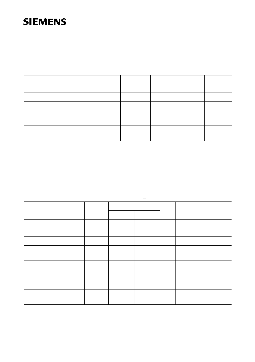
Detailed Register Description . . . . . . . . . . . . . . . . . . . . . . . . . . . . . . . . . . .32
4.1
Register Address Arrangement . . . . . . . . . . . . . . . . . . . . . . . . . . . . . . . . . . .32
4.2
Mode Register (MODR) . . . . . . . . . . . . . . . . . . . . . . . . . . . . . . . . . . . . . . . . .33
4.3
Command Register (CMDR) . . . . . . . . . . . . . . . . . . . . . . . . . . . . . . . . . . . . .34
4.4
Status Register (STAR) . . . . . . . . . . . . . . . . . . . . . . . . . . . . . . . . . . . . . . . . .35
4.5
Interrupt Status Register (ISTA) . . . . . . . . . . . . . . . . . . . . . . . . . . . . . . . . . . .36
4.6
Mask Register (MASK) . . . . . . . . . . . . . . . . . . . . . . . . . . . . . . . . . . . . . . . . . .37
4.7
Memory Access Address/Code Register High (MACH) . . . . . . . . . . . . . . . . .37
4.8
Memory Access Address Register Low (MAAL) . . . . . . . . . . . . . . . . . . . . . .38
4.9
Memory Read Data Register Low (MRDL) . . . . . . . . . . . . . . . . . . . . . . . . . .39
4.10
Memory Read Data Register High (MRDH) . . . . . . . . . . . . . . . . . . . . . . . . . .39
4.11
Memory Write Data Register Low (MWDL) . . . . . . . . . . . . . . . . . . . . . . . . . .39
4.12
Memory Write Data Register High (MWDH) . . . . . . . . . . . . . . . . . . . . . . . . .40
4.13
Input Clock Shift Register Bank ICSR (15:0) . . . . . . . . . . . . . . . . . . . . . . . . .41
4.14
Output Clock Shift Register (OSCR) . . . . . . . . . . . . . . . . . . . . . . . . . . . . . . .42
4.15
Test Register (TSTR) . . . . . . . . . . . . . . . . . . . . . . . . . . . . . . . . . . . . . . . . . . .42
4.16
Frame Evaluation Register Low (FERL) . . . . . . . . . . . . . . . . . . . . . . . . . . . .43
4.17
Frame Evaluation Register High (FERH) . . . . . . . . . . . . . . . . . . . . . . . . . . . .43
5
Electrical Characteristics . . . . . . . . . . . . . . . . . . . . . . . . . . . . . . . . . . . . . .44
6
Package Outlines . . . . . . . . . . . . . . . . . . . . . . . . . . . . . . . . . . . . . . . . . . . . .51
P-MQFP-100-2
Semiconductor Group
4
03.97
Memory Time Switch Extended Large
MTSXL
PEB 2447
Version 1.2
CMOS IC
Type
Ordering Code
Package
PEB 2447 H
Q67103-H6594
P-MQFP-100-2
1
Overview
1.1
Features
∑ Non blocking time/space switch for 4.096- or
8.192-Mbit/s PCM systems
∑ Device clock 16.384 MHz
∑ Switching of up to 2048 incoming PCM channels to
up to 2048 outgoing PCM channels
∑ 32 input and 32 output PCM lines
∑ Tristate function for further expansion and tandem operation
∑
µ
P read access to PCM data
∑ Programmable clock shift with half clock step resolution for input and output
∑ Individual line delay measurement for 6 additional inputs
∑ Individual input offset programmable for 16 PCM inputs
∑ Boundary scan (fully IEEE1149.1 compatible)
∑ Built-in selftest (also usable via boundary scan interface)
∑ 8-bit Intel type demultiplexed
µ
P interface
∑ All registers accessible by direct addressing
∑ In-operation adjustment of bit sampling without bit errors
∑ Low power consumption
∑ Single 5 V power supply
PEB 2447
Overview
Semiconductor Group
5
03.97
1.2
Logic Symbol
Figure 1
Functional Symbol
1.3
General Device Overview
The Siemens Memory Time Switch Extended Large MTSXL (PEB 2447) is a capacity
expansion of the MTSL (PEB 2047). It is a monolithic CMOS switching device capable
of connecting maximally 2048 PCM input time slots to 2048 output time slots. In order to
manage the problem of different line delays, six additional FS inputs can be used as
frame measurement inputs and 16 different input offsets of PCM frames are allowed.
Thus a frame wander can be compensated by adjusting the input offset during operation.
A special circuitry guarantees that no bit error will occur, when reprogramming the input
offsets.
The MTSXL on chip connection memory and data memory are accessed via the 8-bit
standard
µ
P interface (Intel demultiplexed type).
A built-in selftest mechanism ≠ also activated by the
µ
P ≠ ensures proper device
operation in the system.
The PEB 2447 is fabricated using the advanced CMOS technology from Siemens and is
mounted in a P-MQFP-100-2 package. Inputs and outputs are TTL compatible.
PEB 2447
Overview
Semiconductor Group
6
03.97
1.4
Pin Configuration
(top view)
Figure 2
1.5
Pin Definitions and Functions
Pin No.
Symbol
Input (I)
Output (O)
Tristate (T)
Function
14
41
67
V
SS
I
Ground (0 V)
13
40
66
V
DD
I
Supply Voltage: 5 V + 5 %.
ITP09593
IN20
IN21
IN22
IN23
IN24
IN25
IN26
IN27
IN28
IN29
IN30
IN31
CLK
FS0
FS1
FS2
FS3
FS4
FS5
A4
A3
A2
A1
A0
CS
RES
WR
RD
1
80 79 78 77 76 75 74 73 72 71 70 69 68 67 66 65 64 63 62 61 60 59 58 57 56 55 54 53 52 51
2 3 4 5 6 7 8 9 10 11 12 13 14 15 16 17 18 19 20 21 22 23 24 25 26 27 28 29 30
IN19
100
99
IN18
98
IN17
97
IN16
96
IN15
95
IN14
94
IN13
93
IN12
92
IN11
91
IN10
90
IN9
89
IN8
88
IN7
87
IN6
86
IN5
85
IN4
84
IN3
83
IN2
82
IN1
81
IN0
SP
31
D7
32
D6
33
D5
34
D4
35
D3
36
D2
37
D1
38
D0
39
40
41
OUT31
42
OUT30
43
OUT29
44
OUT28
45
OUT27
46
OUT26
47
OUT25
48
OUT24
49
OUT22
50
OUT21
OUT20
OUT19
OUT18
OUT17
OUT16
OUT15
OUT14
OUT13
OUT12
OUT11
OUT10
OUT9
OUT8
OUT7
OUT6
OUT5
OUT4
OUT3
OUT2
OUT1
OUT0
INT
TDO
TMS
TDI
TCK
OUT23
DD
V
V
SS
V
DD
V
SS
Index
Marking
SS
V
V
DD
PEB 2447

PEB 2447
Overview
Semiconductor Group
7
03.97
81
82
83
84
85
86
87
88
89
90
91
92
93
94
95
96
97
98
99
100
1
2
3
4
5
6
7
8
9
10
11
12
IN0
IN1
IN2
IN3
IN4
IN5
IN6
IN7
IN8
IN9
IN10
IN11
IN12
IN13
IN14
IN15
IN16
IN17
IN18
IN19
IN20
IN21
IN22
IN23
IN24
IN25
IN26
IN27
IN28
IN29
IN30
IN31
I
I
I
I
I
I
I
I
I
I
I
I
I
I
I
I
I
I
I
I
I
I
I
I
I
I
I
I
I
I
I
I
PCM Input Ports: Serial data is received at
standard TTL levels.
15
CLK
I
Clock: 16.384 MHz device clock.
1.5
Pin Definitions and Functions (cont'd)
Pin No.
Symbol
Input (I)
Output (O)
Tristate (T)
Function
PEB 2447
Overview
Semiconductor Group
8
03.97
16
17
18
19
20
21
FS0
FS1
FS2
FS3
FS4
FS5
I
I
I
I
I
I
Frame Measuring Inputs: These inputs are used
as frame evaluation inputs.
26
25
24
23
22
A0
A1
A2
A3
A4
I
I
I
I
I
Address Bus Bit 0 to 4: These inputs interface to
the systems address bus to select an internal
register for a read or write access.
27
CS
I
Chip Select: (low active) A low level selects the
MTSXL for a register access operation.
28
RES
I
Reset: A high signal on this Input forces the MTSXL
into reset state.
29
WR
I
Write: (low active) This signal indicates a write
operation.
30
RD
I
Read: (low active) This signal indicates a read
operation.
31
SP
I
Synchronization Pulse: The MTSXL is
synchronized to the PCM system via this line.
39
38
37
36
35
34
33
32
D0
D1
D2
D3
D4
D5
D6
D7
I/O/T
I/O/T
I/O/T
I/O/T
I/O/T
I/O/T
I/O/T
I/O/T
Data Bus: These pins transfer data between the
µ
P
and the MTSXL.
1.5
Pin Definitions and Functions (cont'd)
Pin No.
Symbol
Input (I)
Output (O)
Tristate (T)
Function
PEB 2447
Overview
Semiconductor Group
9
03.97
75
74
73
72
71
70
69
68
OUT0
OUT1
OUT2
OUT3
OUT4
OUT5
OUT6
OUT7
O/T
O/T
O/T
O/T
O/T
O/T
O/T
O/T
PCM Output Port: Serial data is sent by these
lines. These pins can be tristated.
65
64
63
62
61
60
59
58
57
56
55
54
53
52
51
50
49
48
47
46
45
44
43
42
OUT8
OUT9
OUT10
OUT11
OUT12
OUT13
OUT14
OUT15
OUT16
OUT17
OUT18
OUT19
OUT20
OUT21
OUT22
OUT23
OUT24
OUT25
OUT26
OUT27
OUT28
OUT29
OUT30
OUT31
O/T
O/T
O/T
O/T
O/T
O/T
O/T
O/T
O/T
O/T
O/T
O/T
O/T
O/T
O/T
O/T
O/T
O/T
O/T
O/T
O/T
O/T
O/T
O/T
76
INT
O
(Open Drain)
Interrupt Line: Active low.
Reset when reading ISTA
77
TDO
O/T
Test Data Output: In the appropriate TAP
controller state test data, an instruction or the
selftest result is shifted out via this line.
1.5
Pin Definitions and Functions (cont'd)
Pin No.
Symbol
Input (I)
Output (O)
Tristate (T)
Function
PEB 2447
Overview
Semiconductor Group
10
03.97
78
TMS
I
(internal
pull-up)
Test Mode Select: 0 -> 1 transitions on this pin are
required to step through the TAP controller state
machine.
79
TDI
I
(internal
pull-up)
Test Data Input: In the appropriate TAP controller
state test data or an instruction is shifted in via this
line.
80
TCK
I
Test Clock: Single rate test data clock (6.25 MHz)
1.5
Pin Definitions and Functions (cont'd)
Pin No.
Symbol
Input (I)
Output (O)
Tristate (T)
Function

PEB 2447
Functional Description
Semiconductor Group
11
03.97
2
Functional Description
The MTSXL is a memory time switch device. Operating with a device clock of
16.384 MHz it can connect any of 2048 PCM input channels to any of 2048 output
channels.
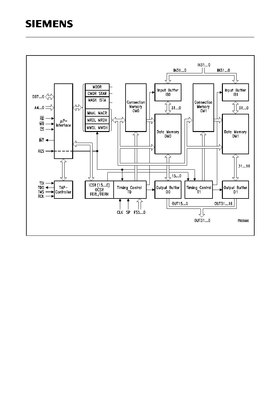
A general block diagram of the MTSXL is shown in figure 3.
2.1
General Operation
The input information of a complete frame is stored twice in the two on-chip 16-kbit data
memories DM 0 and DM 1 (Data Memory 0 and Data Memory 1). The incoming
2048 channels of 8 bits each are written in sequence into fixed positions of DM 0 and
DM 1. This is controlled by the input counter in the timing control block with a 8 kHz
repetition rate.
For outputting, two connection memories (CM 0 and CM 1) are read in sequence
synchronously. Each entry in the connection memory CM 0 / CM 1 points to a location
in data memory DM 0 / DM 1. The byte in this data memory location is transferred into
the current output time slot. The read access to the CM's is controlled by an output
counter. CM 0 supplies the PCM data for outputs OUT0 to OUT15, CM 1 supplies the
PCM data for outputs OUT16 to OUT31.
PEB 2447
Functional Description
Semiconductor Group
12
03.97
Figure 3
Block Diagram of MTSXL
The synchronization of the input and output counters is achieved by a rising edge of the
sync pulse SP, which is always sampled with the falling edge of the device clock.
Different modes of operation are configurable at the PCM interfaces (see table 9).
Furthermore, 16 PCM input lines can be aligned with individual clock shift values to
compensate different line delays. If 32 inputs are used, one clock shift value controls two
ports at the same time.
Shifting of the output frame is also possible, but all output lines are affected the same
way.
The input lines FS0 to FS5 are used as frame measurement inputs. After synchronizing
the device by the SP pulse the FS inputs can be evaluated on a per port basis. This
evaluation procedure is started by a microprocessor command. As a result the input
counter value on the rising edge of the FS signal can be read from an internal register.
Thus delay compensation is easily managed by programming appropriate clock shift
values and/or a possible software offset.

PEB 2447
Functional Description
Semiconductor Group
13
03.97
During operation of the chip a frame length check is also supplied, which controls correct
synchronization by the SP pulse and generates an interrupt in case of lost or achieved
synchronization.
The unused output ports are tristated by mode selection, whereas unused time slots are
tristated by an additional bit in the control memory. By using this tristate capability the
MTSXL can be easily expanded to a time switch of any size.
The standard 8-bit
µ
P interface can communicate with Intel demultiplexed
microprocessors. It gives access to the internal registers and to the control and data
memory. All registers are directly addressable. The memories are accessed by a simple
four byte indirect access method.
2.2
Special Functions
The activity of all special functions can be read in the status register. Completion of these
functions is indicated by interrupts.
2.2.1
Control Memory Reset
Initialization of the device after a hardware reset (RES) is easily done with a
µ
P
command "control memory reset". After finishing this procedure all control memory
channels contain the information "tristated". Apart from this tristate information the
contents of the C Memory is undefined.
2.2.2
Evaluate Frame Measurement Signal
A command including the address (0 ... 5) will be given by the
µ
P. The rising edge of the
corresponding frame measurement signal (FS0 ... FS5) will be evaluated. The exact
timing of the FS edge can then be read from an internal 12-bit register (resolution of a
complete 8 kHz frame in half 16 MHz clock periods).
2.2.3
MTSXL Selftest
The switching path of the MTSXL including input buffer, data memory, control memory,
output buffer and timing control can be tested in the system by a 2-step built-in selftest.
Activating this mechanism takes 2
◊
0.625 ms (16.384 MHz). Finally the result "selftest
ok/selftest not ok" can be read from the internal status register.
After test completion the control memory has also been reset (contains the information
tristated).
The selftest can also be started and checked via the boundary scan interface.
Note: For correct execution of the built-in selftest the MTSXL needs a value of
ICSR = 00. If MODR:PSB = 0 (e.g. after hardware reset) this value is programmed
automatically after start of the selftest procedure. If ICSR does not contain "00"
with MODR:PSB = 1 the selftest will fail.

PEB 2447
Functional Description
Semiconductor Group
14
03.97
2.3
Boundary Scan and TAP Controller
2.3.1
Boundary Scan
The MTSXL provides fully IEEE Std. 1149.1 compatible boundary scan support
consisting of
≠ a complete boundary scan
≠ a test access port controller (TAP controller)
≠ four dedicated pins (TCK, TMS, TDI, TDO)
≠ a 32 bit IDCODE register
All pins except power supply and ground are included in the boundary scan. Depending
on the pin functionality one, two or three boundary scan cells are provided:
When the TAP controller is in the appropriate mode data is shifted into / out of the
boundary scan via the pins TDI / TDO using the 6.25 MHz clock on pin TCK.
The MTSXL pins are included in the boundary scan in the following sequence:
Table 1
Boundary Scan Cell Type
Pin Type
Number of Boundary Scan Cells
Usage
Input
1
Input
Output
2
Output, enable
I/O
3
Input, output, enable
Table 2
Boundary Scan Sequence
Boundary Scan
Number TDI ->
Pin
Number
Pin
Name
Type
Number of Scan
Cells
Default
Value
1
81
IN0
I
1
0
2
82
IN1
I
1
0
3
83
IN2
I
1
1
4
84
IN3
I
1
0
5
85
IN4
I
1
0
6
86
IN5
I
1
0
7
87
IN6
I
1
0
8
88
IN7
I
1
0
9
89
IN8
I
1
0
10
90
IN9
I
1
0
11
91
IN10
I
1
0
PEB 2447
Functional Description
Semiconductor Group
15
03.97
12
92
IN11
I
1
0
13
93
IN12
I
1
0
14
94
IN13
I
1
0
15
95
IN14
I
1
1
16
96
IN15
I
1
0
17
97
IN16
I
1
0
18
98
IN17
I
1
1
19
99
IN18
I
1
0
20
100
IN19
I
1
1
21
1
IN20
I
1
0
22
2
IN21
I
1
0
23
3
IN22
I
1
0
24
4
IN23
I
1
0
25
5
IN24
I
1
1
26
6
IN25
I
1
0
27
7
IN26
I
1
0
28
8
IN27
I
1
0
29
9
IN28
I
1
0
30
10
IN29
I
1
0
31
11
IN30
I
1
1
32
12
IN31
I
1
1
33
15
CLK
I
1
0
34
16
FS0
I
1
0
35
17
FS1
I
1
0
36
18
FS2
I
1
0
37
19
FS3
I
1
0
38
20
FS4
I
1
0
39
21
FS5
I
1
0
40
22
A4
I
1
0
41
23
A3
I
1
0
42
24
A2
I
1
0
Table 2
Boundary Scan Sequence (cont'd)
Boundary Scan
Number TDI ->
Pin
Number
Pin
Name
Type
Number of Scan
Cells
Default
Value
PEB 2447
Functional Description
Semiconductor Group
16
03.97
43
25
A1
I
1
0
44
26
A0
I
1
0
45
27
CS
I
1
0
46
28
RES
I
1
0
47
29
WR
I
1
0
48
30
RD
I
1
0
49
31
SP
I
1
0
50
32
AD7
IO
3
000
51
33
AD6
IO
3
000
52
34
AD5
IO
3
000
53
35
AD4
IO
3
000
54
36
AD3
IO
3
000
55
37
AD2
IO
3
000
56
38
AD1
IO
3
000
57
39
AD0
IO
3
000
58
42
OUT31
O
2
00
59
43
OUT30
O
2
00
60
44
OUT29
O
2
00
61
45
OUT28
O
2
00
62
46
OUT27
O
2
00
63
47
OUT26
O
2
00
64
48
OUT25
O
2
00
65
49
OUT24
O
2
00
66
50
OUT23
O
2
00
67
51
OUT22
O
2
00
68
52
OUT21
O
2
00
69
53
OUT20
O
2
00
70
54
OUT19
O
2
00
71
55
OUT18
O
2
00
72
56
OUT17
O
2
00
73
57
OUT16
O
2
00
Table 2
Boundary Scan Sequence (cont'd)
Boundary Scan
Number TDI ->
Pin
Number
Pin
Name
Type
Number of Scan
Cells
Default
Value
PEB 2447
Functional Description
Semiconductor Group
17
03.97
74
58
OUT15
O
2
00
75
59
OUT14
O
2
00
76
60
OUT13
O
2
00
77
61
OUT12
O
2
00
78
62
OUT11
O
2
00
79
63
OUT10
O
2
00
80
64
OUT9
O
2
00
81
65
OUT8
O
2
00
82
68
OUT7
O
2
00
83
69
OUT6
O
2
00
84
70
OUT5
O
2
00
85
71
OUT4
O
2
00
86
72
OUT3
O
2
00
87
73
OUT2
O
2
00
88
74
OUT1
O
2
00
89
75
OUT0
O
2
00
90
76
INT
O
2
00
Table 2
Boundary Scan Sequence (cont'd)
Boundary Scan
Number TDI ->
Pin
Number
Pin
Name
Type
Number of Scan
Cells
Default
Value

PEB 2447
Functional Description
Semiconductor Group
18
03.97
2.3.2
TAP Controller
The TAP controller implements a state machine defined in the JTAG standard
IEEE1149.1. The instruction register of the controller is extended to 4 bits in order to
increase the number of instructions. This is necessary for the use of the build in selftest
procedure via the boundary scan interface:
The standard instructions are implemented according to the JTAG standard, just the
instruction register is extended to 4 bits. At the new instructions TAP_TEST1.. 8 special
internal test signals are activated during the state "RUN TEST / IDLE".
The MTSXL only uses TAP_TEST1 and TAP_TEST2 according to table 3.
Table 3
Instruction Code of 4 Bit TAP Controller
Instruction
Code
EXTEST
0000
INTEST
0001
SAMPLE / PRELOAD
0010
IDCODE
0011
BYPASS
11xx
TAP_TEST1:
Start built in self test
0100
TAP_TEST2:
Write selftest control register
0101
TAP_TEST3
0110
TAP_TEST4
0111
TAP_TEST5
1000
TAP_TEST6
1001
TAP_TEST7
1010
TAP_TEST8
1011

PEB 2447
Functional Description
Semiconductor Group
19
03.97
The extended TAP controller uses a modified data path:
When TAP_TEST1 / 2 is activated the data path is set to shift the result of the selftest
procedure (bit STAR:STOK) out through the TDO pin.
2.3.3
Use of Built in Selftest via the Boundary Scan Interface
The built in self test is used by the following steps:
≠ The instruction TAP_TEST2 is shifted into the TAP controller (see figure 4)
≠ STP command is shifted into the selftest control register (see table 5 and figure 5)
≠ The instruction TAP_TEST1 is shifted into the TAP controller to start the selftest
(see figure 6) after 10240 TCK periods:
≠ Bit STAR:STOK can be shifted out (see figure 7)
.
Note: ST [2:0] represent the bits CMDR:STP2..0 but do not overwrite them.
Table 4
Data Path of 4 Bit TAP Controller
Instruction Code
Input
Data Path
Output
11xx
TDI
TDO
00xx
BSOUT
TDO
0011
BSOUT_ID
TDO
01xx
TDI2: STAR:STOK (internal)
TDO
10xx
TDI3: VSS (not used, internal)
TDO
Table 5
4 Bit Selftest Control Register
Bit
Function
ST [0]
CMDR:STP0
ST [1]
CMDR:STP1
ST [2]
CMDR:STP2
ST [3]
"1" built in selftest
"0" no built in selftest

PEB 2447
Functional Description
Semiconductor Group
20
03.97
The TAP controller state machine passes through the different states according to
figures 4 to 7.
Note: The state coding is only described for explanation purposes, it is externally not
visible.
Table 6
States of TAP Controller (explanation for figures 4 to 7)
Controller State
State Code
Exit2-DR
0
Exit1-DR
1
Shift-DR
2
Pause-DR
3
Select-IR-Scan
4
Update-DR
5
Capture-DR
6
Select-DR-Scan
7
Exit2-IR
8
Exit1-IR
9
Shift-IR
A
Pause-IR
B
Run-Test / Idle
C
Update-IR
D
Capture-IR
E
Test-Logic-Reset
F
PEB 2447
Functional Description
Semiconductor Group
21
03.97
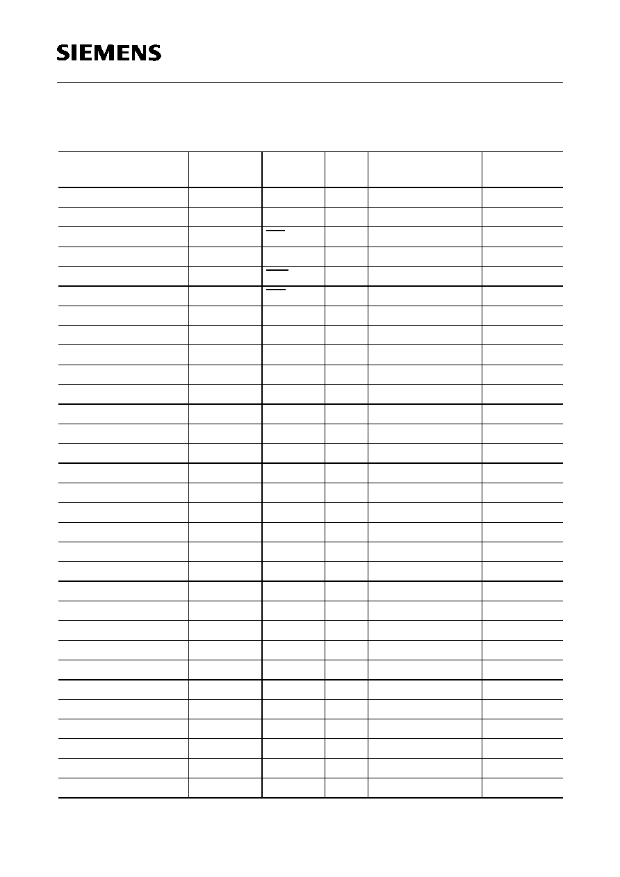
Figure 4
Starting Instruction "TAP_TEST2" (code 0101)
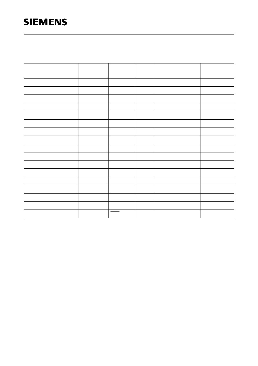
Figure 5
Writing Selftest Control Register
PEB 2447
Functional Description
Semiconductor Group
22
03.97
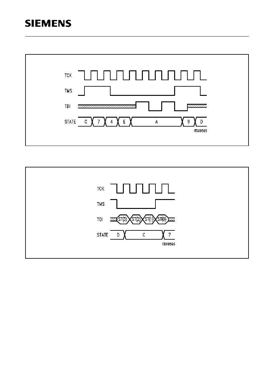
Figure 6
Start of Built in Selftest (instruction TAP_TEST1, code 0100)
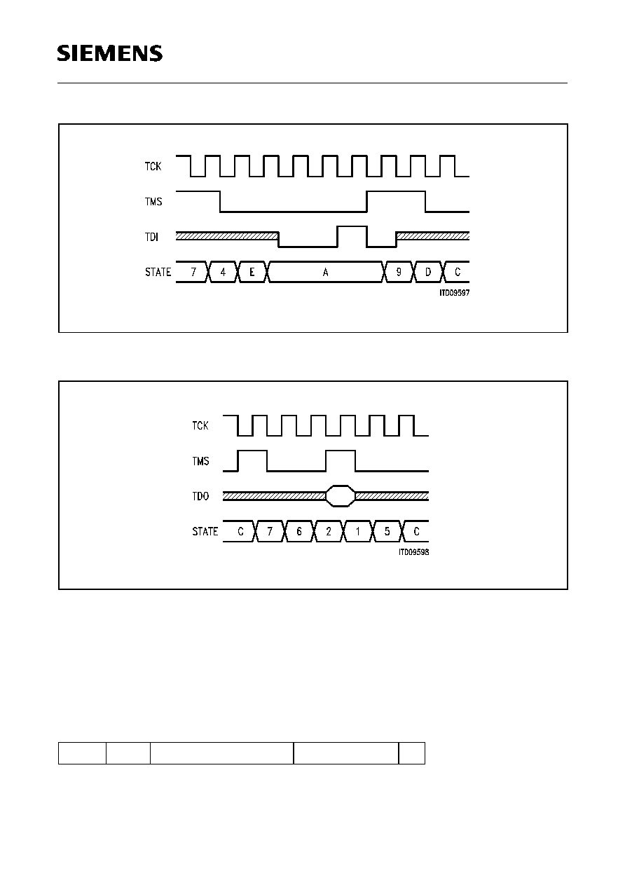
Figure 7
Readout of Selftest Result (after 10240 TCK periods)
Note: After the use of the selftest procedure over the
µ
P Interface or the boundary scan
interface a hardware reset is necessary before the selftest procedure can be
started again over the other interface.
2.3.4
IDCODE
The manufacturer code for MTSXL is according to table 2:
V1.2:
0010 0000 0000 0010 0101
0000 1000 001
1

PEB 2447
Operational Description
Semiconductor Group
23
03.97
3
Operational Description
3.1
Initialization Procedure
For a proper initialization of the MTSXL the following procedure is recommended:
First a reset pulse (RES) of at least two CLK clock periods has to be applied. All registers
contain now their reset values. In the next step the connection memories CM0/1 are
initialized by the commands CMDR:STP (1:0) = 01 (CM reset) or CMDR:STP
(2:0) = 011 / 111 (MTSXL selftest).
After having programmed a CM reset command, it takes 4096 clock periods until all
tristate control entries in the CM contain the value "1" (tristated).
If a selftest command was given, it takes 10 240 clock periods to achieve the same
effect. Furthermore the register bit STAR:STOK (selftest o.k.) should read "1" in this
case, in order to prove that there is no fault on the chip. The selftest command must be
given twice: the upper half of data memory (DM0, DM1) is tested when setting
CMDR:STP (2:1) = 01, the lower half of DM0, DM1 is tested by setting CMDR:STP
(2:1) = 11 (see table 10).
The activity of the procedures can be monitored in STAR:PACT and an interrupt will
indicate their completion.
In all cases it is important, that the outputs are tristated by MODR:PSB = 0.
3.2
Operation Mode
The operation mode of the device is fixed by programming MODR:MD (1:0) (see
table 9).
3.3
Indirect Access Registers
The connection memories and data memories are accessible through the indirect access
registers MACH, MAAL, MRDH, MRDL, MWDH and MWDL. An indirect access is
actually started by writing register MACH (Memory Access Address/Code Register
High). The code value inherent in this register defines, what action has to be performed.
The low byte of the complete access address must be programmed to MAAL (Memory
Access Address Register Low) before writing to MACH. If data are necessary to perform
the access (e.g. in write operations), they have to be entered into MWDH (Memory Write
Data Register High) and MWDL (Memory Write Data Register Low) before. In read
accesses the corresponding registers MRDH (Memory Read Data Register High) and
MRDL (Memory Read Data Register Low) contain the required information after the
internal read process is completed.
PEB 2447
Operational Description
Semiconductor Group
24
03.97
Typical Write Operation:
Typical Read Operation:
WR MWDL
WR MAAL
WR MWDH
WR MACH
WR MAAL
RD STAR; STAR:MAC = 0
WR MACH
RD MRDL
RD STAR; STAR:MAC = 0
RD MRDH
3.4
Frame Evaluation
If the device is in synchronized state (STAR:PSS = 1) and for example the command
"frame evaluation at FS5" (CMDR = 58
H
) is programmed, the second following rising
edge of FS5 is evaluated and creates the following result in register FERH:FERL (see
also table 15):
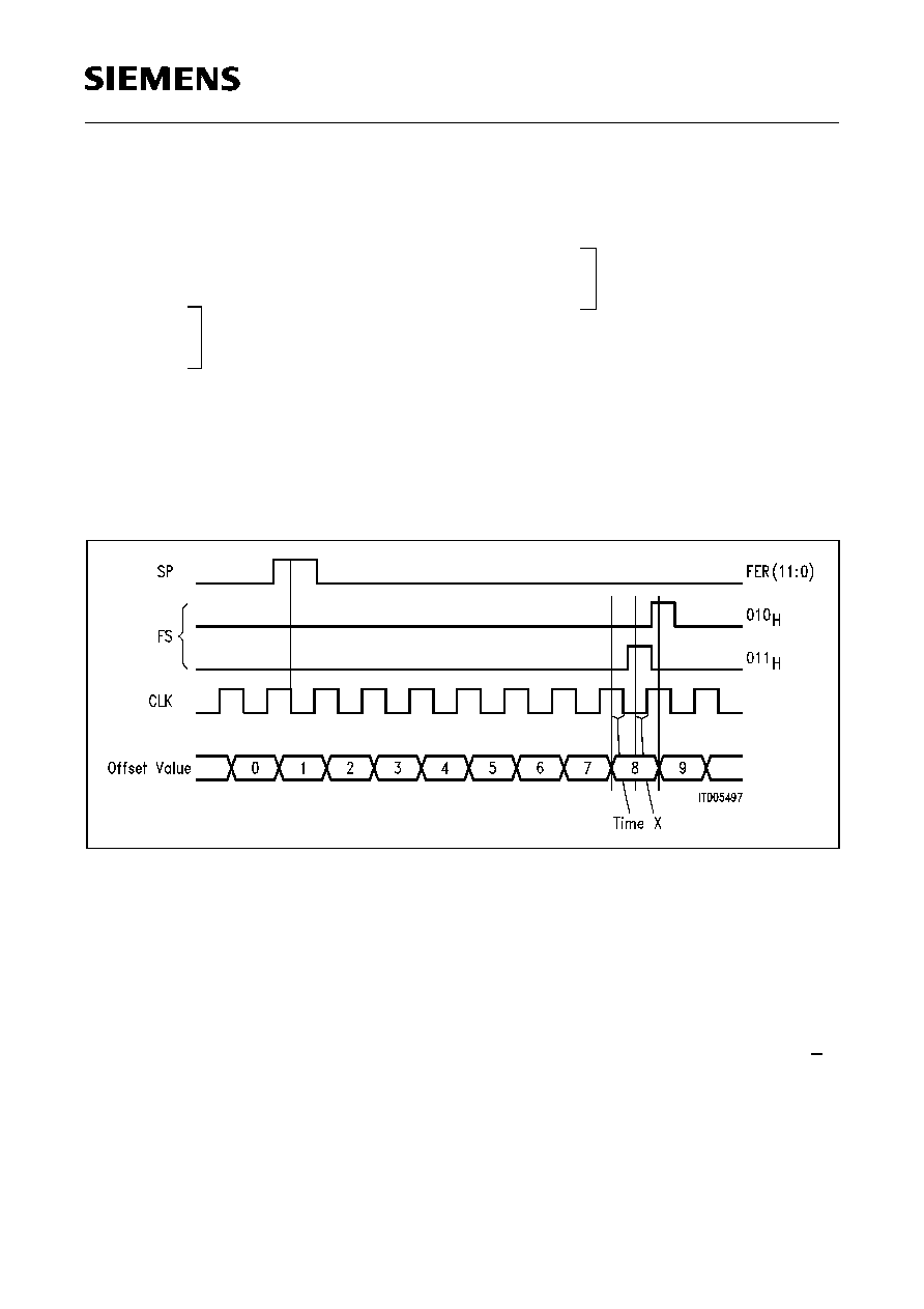
Figure 8
Frame Evaluation
Note: The frame evaluation procedure gives (roughly) the number to be programmed in
ICSR (after inversion of FER0): FEV 11..1 give the number of complete CLK
periods; FEV 0 gives the sampling edge (falling / rising). Due to the internal delay
in the MTSXL the sampling region and therefor the result in FEV 11..1 is shifted
against CLK for a time
"
X" which is uncertain between 0 < X < 13 ns. If the rising
edge of FS occurs in that uncertain region the value of FER 11..1 might vary + 1
(FER 0 inverted before!).
PEB 2447
Operational Description
Semiconductor Group
25
03.97
3.5
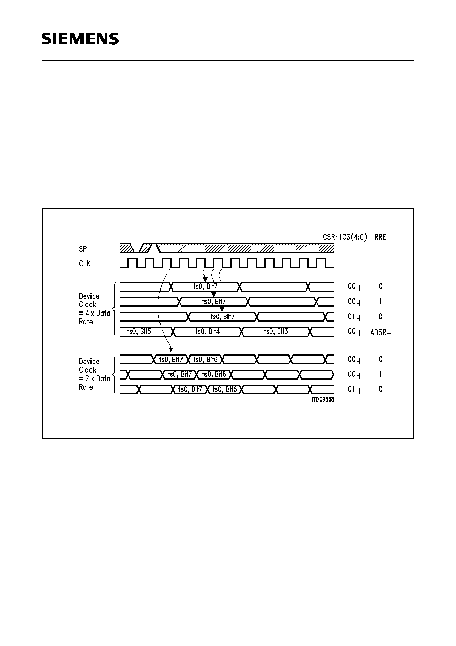
Input Offset and Output Offset
Based on the results of the frame evaluation procedures the input offsets can be
adjusted by programming ICSR 7..0 corresponding to inputs IN 7..0. If data
oversampling is used, the values of ICSR 7..0 can be adjusted within some limits during
operation without producing bit errors:
≠ clockrate = 2
◊
datarate
possible adjustment is one half clock period forward or backward.
≠ clockrate = 4
◊
datarate
possible adjustment is one clock period backward or two clock periods forward.
Figure 9
Input Timing
PEB 2447
Operational Description
Semiconductor Group
26
03.97
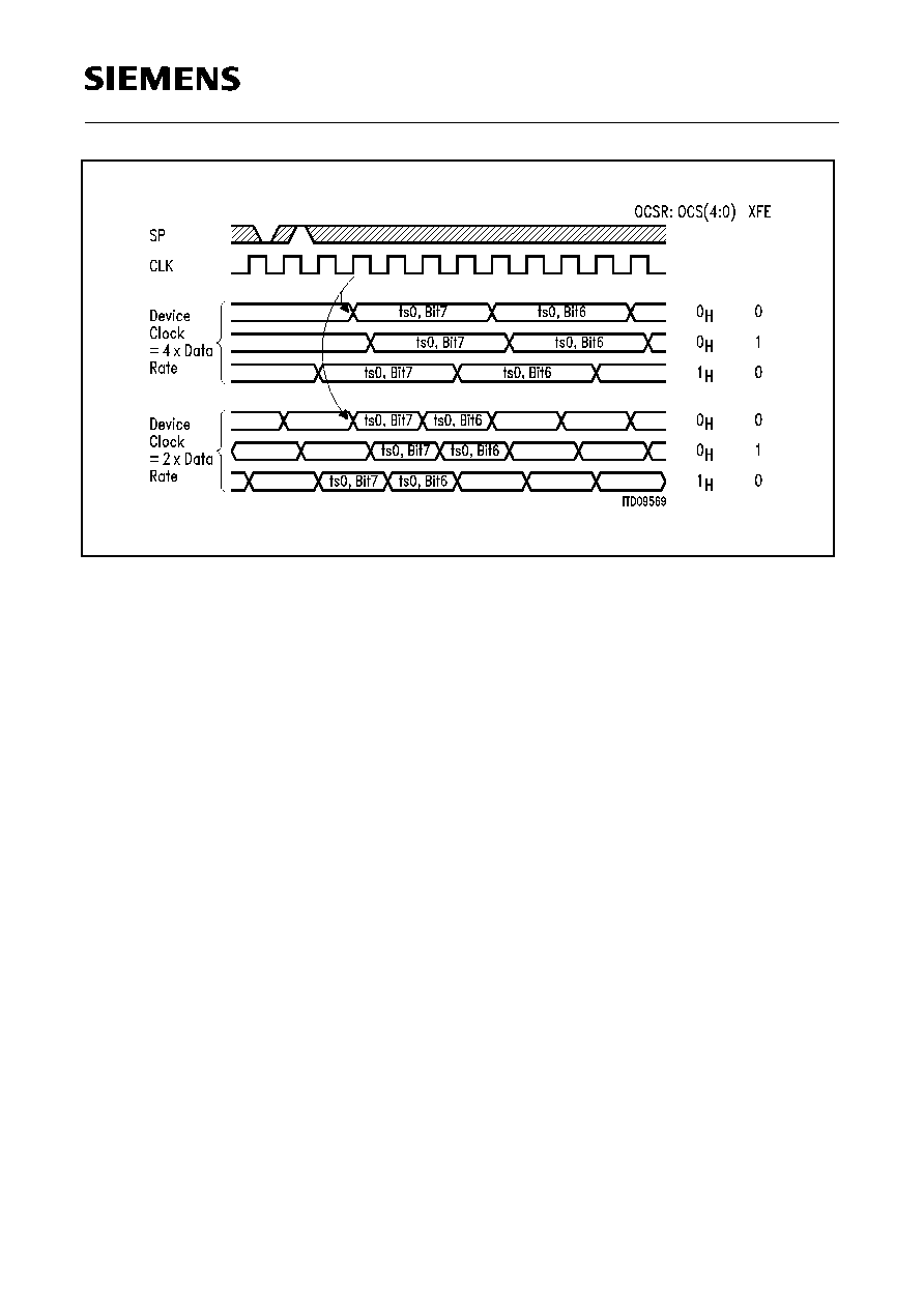
Figure 10
Output Timing
The output offset is the same for all output lines and is fixed in register OCSR.
PEB 2447
Operational Description
Semiconductor Group
27
03.97
3.6
Frame Delay
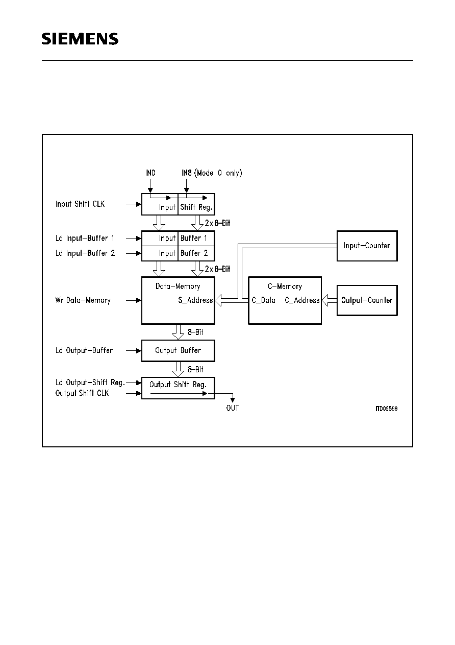
Figure 11 shows a functional description of the Serial Input, Data Memory and Serial
Output.
Figure 11
Internal Processing of Serial Data
In mode 0 for example inputs 0 and 8 are both connected to the input shift register. In
mode 1 and 3 only input 0 is used and two time slots are always processed together.
PEB 2447
Operational Description
Semiconductor Group
28
03.97
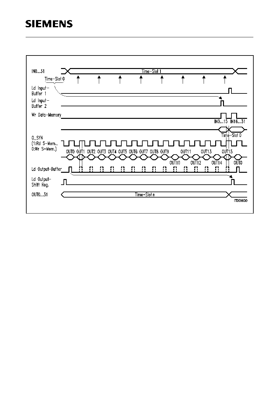
Figure 12
Internal Control Signals Mode 0 (OCSR = 0)
Note: O_SYN is a control signal for the synchronization of RD and WR access to the
data memory and not important for the external functionality. O_SYN frequency is
f
CLK
/ 2.
This figure shows that the inputs IN0 .. IN15 are written into the data memory at the same
time whereas IN16 .. IN31 are written one O_SYN period (= 2 CLK periods) later. The
value of ICSR 0..15 shifts the sampling points and the signal "Ld Inp Buffer 1" later in
time (rightwards), the signals "Ld Inp Buffer 2" and "Wr S Memory" remain constant. In
this example with OCSR = 0 the lower Inputs IN0 .. IN15 are written into data memory
before Out15 (and Out31) is read.
With OCSR > 0 all Output Signals (Ld Outp Buffer and following) including the data
(OUT0..15) on the internal data transfer bus is shifted earlier in time (leftwards). Therefor
the data is read out of the data memory earlier.
Due to the internal timing the frame delay is depending on the programmed input / output
time slots and OCSR. The internal delay (number of time slots) can be deduced from
figure 12 and is shown in table 7.
PEB 2447
Operational Description
Semiconductor Group
29
03.97
If the offset of output time slot to input time slot is greater or equal to the internal delay
due to table 7 the transmission of data is within the same frame (frame delay 0).
If the offset is smaller or even negative the transmission is in the next frame (frame
delay 1).
Frame delay 1 also occurs when the programmed connection overrides the frame end
(TS63 in Mode 0).
If the offset is smaller and overrides the frame end at the same time the frame delay is 2.
Examples: Connection
IN1 ts1
-> OUT1 ts 5
(Offset 4ts) :
frame delay 0
(OCSR=0)
IN1 ts1
-> OUT1 ts 3
(Offset 2ts) :
frame delay 1
IN1 ts62 -> OUT31 ts 0
(Offset 2ts) :
frame delay 1
IN1 ts62 -> OUT1 ts 1
(Offset 3ts) :
frame delay 2
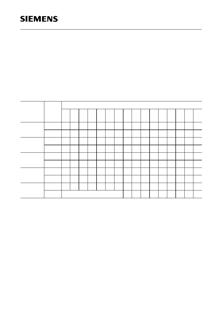
Table 7
Time Slots Delay Mode 0
OCS(4:0)
IN
Outputs
0
16
1
17
2
18
3
19
4
20
5
21
6
22
7
23
8
24
9
25
10
26
11
27
12
28
13
29
14
30
15
31
0
0 - 15
3
3
3
3
3
3
3
3
3
3
3
3
3
3
3
2
16 - 31 3
3
3
3
3
3
3
3
3
3
3
3
3
3
3
3
1
0 - 15
3
3
3
3
3
3
3
3
3
3
3
3
3
3
3
3
16 - 31 4
3
3
3
3
3
3
3
3
3
3
3
3
3
3
3
2
0 - 15
4
3
3
3
3
3
3
3
3
3
3
3
3
3
3
3
16 - 31 4
4
3
3
3
3
3
3
3
3
3
3
3
3
3
3
3
0 - 15
4
4
3
3
3
3
3
3
3
3
3
3
3
3
3
3
16 - 31 4
4
4
3
3
3
3
3
3
3
3
3
3
3
3
3
.
.
Maximum delay 4 time slots

PEB 2447
Operational Description
Semiconductor Group
30
03.97
Figure 13
Internal Control Signals Mode 1/3 (OCSR = 0)
PEB 2447
Operational Description
Semiconductor Group
31
03.97
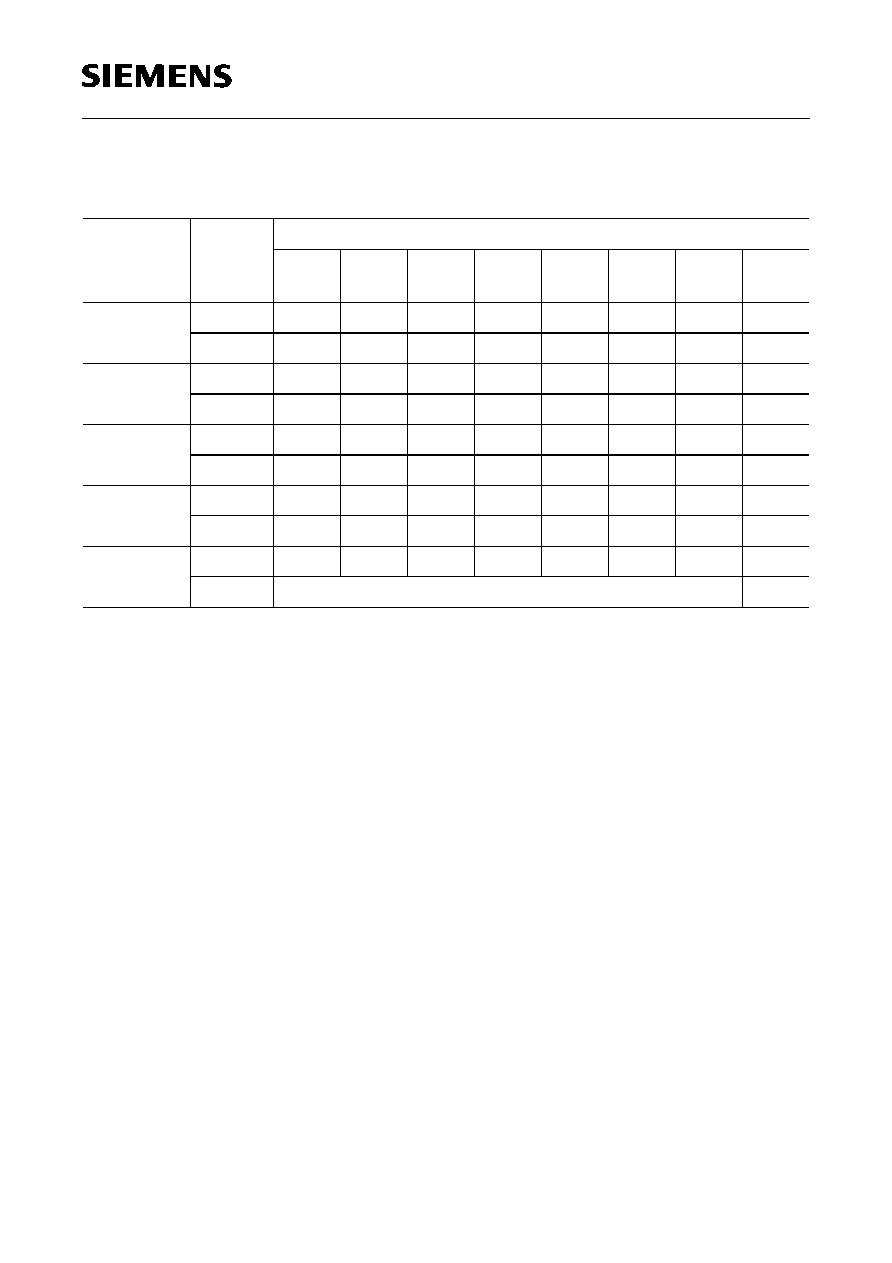
Note: The time slot delays given in table 8 are valid only for even input time slots; for odd
input time slots all delays have to be reduced by 1 time slots.
Table 8
Time Slot Delay Mode 1 / 3 (deduced from figure 13, only Input time slots 0, 2, 4,..)
OCS(4:0)
IN
Outputs
0
16
1
17
2
18
3
19
4
20
5
21
6
22
7
23
0
0 - 7
5
5
5
5
5
5
5
4
16 - 23
5
5
5
5
5
5
5
5
1
0 - 7
5
5
5
5
5
5
5
5
16 - 23
6
5
5
5
5
5
5
5
2
0 - 7
6
5
5
5
5
5
5
5
16 - 23
6
6
5
5
5
5
5
5
3
0 - 7
6
6
5
5
5
5
5
5
16 - 23
6
6
6
5
5
5
5
5
.
.
Maximum delay 6 time slots
PEB 2447
Detailed Register Description
Semiconductor Group
32
03.97
4
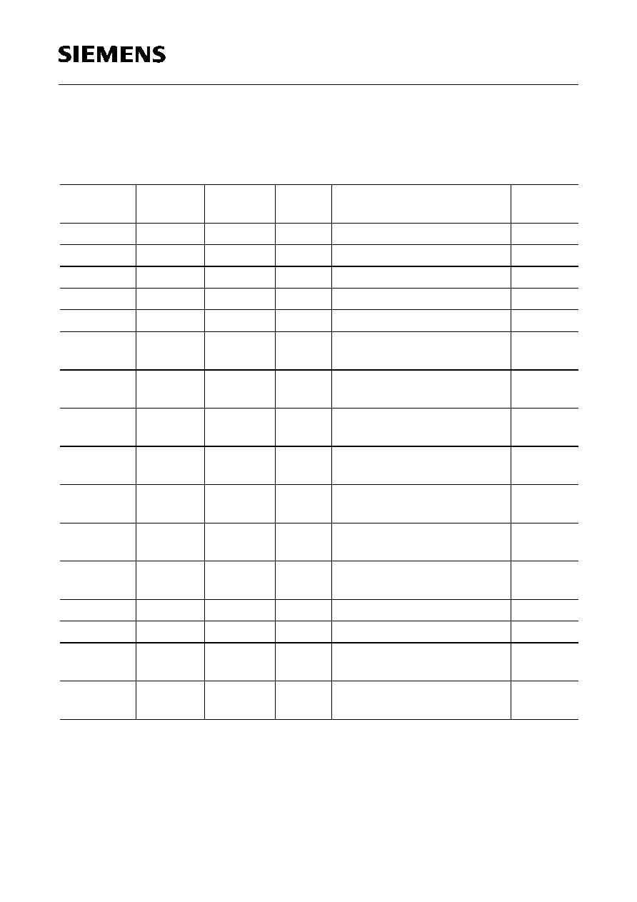
Detailed Register Description
4.1
Register Address Arrangement
Reg.
Name
Access
Address
A4..0
Reset
Value
Comment
Refer to
page
MODR
RD/WR
00
H
00
H
Mode register
33
CMDR
WR
01
H
00
H
Command register
34
STAR
RD
01
H
01
H
Status register
35
ISTA
RD
02
H
00
H
Interrupt status register
36
MASK
WR
02
H
0F
H
Mask register
37
MACH
RD/WR
04
H
0X
H
Memory access
address/code register high
37
MAAL
RD/WR
03
H
XX
H
Memory access address
register low
38
MRDL
RD/WR
05
H
XX
H
Memory read data register
low
39
MRDH
RD/WR
06
H
0X
H
Memory read data register
high
39
MWDL
RD/WR
07
H
XX
H
Memory write data register
low
39
MWDH
RD/WR
08
H
XX
H
Memory write data register
high
40
ICSR
(15:0)
RD/WR
10
H
.. 1F
H
00
H
Input clock shift register
bank
41
OSCR
RD/WR
0B
H
00
H
Output clock shift register
42
TSTR
RD/WR
0C
H
C0
H
Test register
42
FERL
RD
0E
H
XX
H
Frame evaluation register
low
43
FERH
RD
0F
H
XX
H
Frame evaluation register
high
43
PEB 2447
Detailed Register Description
Semiconductor Group
33
03.97
4.2
Mode Register (MODR)
Access in demultiplexed
µ
P-interface mode:
Read/write, address:
00
H
Reset value:
00
H
PSB
PCM Stand By; a logical 0 switches the PCM interface outputs to
high impedance.
MD1 ... MD0
Mode; these bits define the chip operation mode according
to the following table:
Note: *
)
In mode 3 the PCM lines OUT(n+16) drive the inverted values of lines OUT(n)
or are tristated, if the corresponding PCM line is tristated.
Bit 7
Bit 0
PSB
0
0
0
0
0
MD1
MD0
Table 9
Operation Modes
Operation
Mode
Mode Bits
MD1 MD0
Input # of
Ports
Input Data
Rate [MHz]
Output # of
Ports
Output Data
Rate [MHz]
Mode 0
0 0
32
4.096
32
4.096
Mode 1
0 1
16
8.192
16
8.192
Mode 3
1 1
16
8.192
16
16
*
)
8.192
8.192

PEB 2447
Detailed Register Description
Semiconductor Group
34
03.97
4.3
Command Register (CMDR)
Access in demultiplexed
µ
P-interface mode:
Write, address:
01
H
Reset Value:
00
H
(not readable)
FSAD2..0
Frame Synchronization signal Address 2 to 0; Address of the
chosen FS signal 5 to 0 to be evaluated by the procedure started by
SFE.
SFE
Start Frame Evaluation; a one in this bit position starts the frame
evaluation procedure. A read operation on register FER will stop an
unfinished frame evaluation procedure.
STP2..0
Start Procedure.
The following procedures can be activated by these bits:
X: don't care
Note: Before activating one of these procedures MODR:PSB has to be set to 0. During
selftest or CM reset the device will ignore the external synchronization pulse and
the user has no access to the internal data memory.
Bit 7
Bit 0
0
FSAD2 FSAD1 FSAD0
SFE
STP2
STP1
STP0
Table 10
STP Commands
STP2
STP1
STP0
Function
X
X
0
1
X
0
1
1
0
1
1
1
No operation
Start control memory reset procedure
Start selftest procedure (1st part)
Start selftest procedure (2nd part)

PEB 2447
Detailed Register Description
Semiconductor Group
35
03.97
4.4
Status Register (STAR)
Access in demultiplexed
µ
P-interface mode:
Read, address:
01
H
Reset value:
01
H
FSAD2..0
Frame Synchronization signal Address: see CMDR.
MAC
Memory Access Active; an indirect memory access is active, if this
bit is "1", all memory access registers must not be written until
MAC = "0".
PACT
Procedure Active; one of the procedures started by the
µ
P (selftest,
CM reset or frame evaluation) is active.
PSS
PCM Synchronization Status
1: the PCM interface is synchronized
0: the PCM interface is not synchronized. (see note in chapter 4.5)
STOK
Selftest O.K.; after a selftest procedure this bit is set to 1, if no faults
are detected.
Note: This bit is only valid, if no power failure or inappropriate clocking occurred during
the test (see ISTA:IR); this bit is set to 1 by a start selftest command or by
hardware reset.
Bit 7
Bit 0
0
FSAD2 FSAD1 FSAD0
MAC
PACT
PSS
STOK

PEB 2447
Detailed Register Description
Semiconductor Group
36
03.97
4.5
Interrupt Status Register (ISTA)
Access in demultiplexed
µ
P-interface mode:
Read, address:
02
H
Reset value:
00
H
FEC
Frame Evaluation Completed; the indirect register FER contains a
valid offset and can be read.
PC
Procedure Completed; the procedure started from the command
register (CM reset or MTSXL selftest) is finished.
IR
Initialization Request. The connection memory has to be
programmed due to a loss of data (IR = 1). The IR bit is set after
power failure or inappropriate clocking. It can only be retriggered
again after a selftest or CM reset procedure.
PFI
PCM Framing Interrupt; this bit being logical 1 indicates the loss or
gain of synchronization. Synchronization is considered lost by the
MTSXL if the SP signal is not repeated within the correct period.
Synchronization is considered achieved, if two consecutive SP
pulses with the correct period have been received.
Any interrupt will activate the INT line if it is not masked. All interrupt bits and the INT line
are reset when reading ISTA.
Note 1: All interrupts and the INT line are cleared with reset.
Note 2: If the SP signal is repeated within a multiple of frame length
(e.g. 2
◊
or 4
◊
125
µ
s) but at correct phase:
≠ the MTSXL works correctly because the internal counters run autonomously
and are synchronized within correct phase.
≠ the PFI interrupt does not occur because this situation is internally handled as
"loss of synchronization" and this situation does not change.
Note 3: During selftest no PFI interrupt will occur.
Bit 7
Bit 0
0
0
0
0
FEC
PC
IR
PFI
PEB 2447
Detailed Register Description
Semiconductor Group
37
03.97
4.6
Mask Register (MASK)
Access in demultiplexed
µ
P-interface mode:
Write, address:
02
H
Reset value:
0F
H
A logical 1 disables the corresponding interrupt as described in ISTA from activating the
INT pin. A masked interrupt (bit set to "1") is stored internally and indicated, when reading
ISTA. It is also reset in this case.
4.7
Memory Access Address/Code Register High (MACH)
Access in demultiplexed
µ
P-interface mode:
Read/write, address:
04
H
Reset value:
0X
H
A write access (rising edge of WR or CS) to this register starts an indirect access to a
memory location.
MAC2..0
Memory Access Code values to determine the type of access
to/from control and data memory locations. See table 11 for all
possible code values.
Note: A write & read control memory command actually writes a specific CM location
and reads the same location in a second access.
MA10..8
Memory Address (most significant) bits 10 to 8; refer to register
MAAL
Bit 7
Bit 0
0
0
0
0
FEC
PC
IR
PFI
Bit 7
Bit 0
MAC2
MAC1
MAC0
0
0
MA10
MA9
MA8
Table 11
Memory Access Codes
MAC2
MAC1
MAC0
Function
Max. Access Time
Clock Periods
0
0
0
0
1
0
0
1
1
0
0
1
1
0
0
No operation
Write control memory
Write & read control memory
Read control memory
Read data memory
≠
4.5
6.5
4.5
8.5
All other combinations are not allowed
PEB 2447
Detailed Register Description
Semiconductor Group
38
03.97
4.8
Memory Access Address Register Low (MAAL)
Access in a demultiplexed
µ
P-interface mode:
Read/write, address:
03
H
Reset value:
XX
H
MA7..0
Memory Address bits 7 to 0; the complete memory address is the
concatenation of MA10..0.
If the value MA(10:0) is used as a control memory address, each address corresponds
to a single output time slot (see table 12):
Note: Port(m) means, that this port drives the inverted data values of port (m-8). For the
operation "Read Data Memory" MA10..0 are used as data memory addresses with
the same mapping to the input time slots as listed in the above table.
Bit 7
Bit 0
MA7
MA6
MA5
MA4
MA3
MA2
MA1
MA0
Table 12
Output Time Slot Mapping
Mode
Valid for
Output (Ports)
0
MA10 MA9 MA8 MA7 MA6 MA5 MA4 MA3 MA2 MA1 MA0
OUT (31:0) =
Port (31:0)
Time Slot Number
Port Number
1
MA10 MA9 MA8 MA7 MA6 MA5 MA4 MA3 MA2 MA1 MA0
OUT (7:0) =
Port (7:0)
OUT (23:16) =
Port (15:8)
Time Slot Number6..1
PN3 TS0
PN2..0
3
MA10 MA9 MA8 MA7 MA6 MA5 MA4 MA3 MA2 MA1 MA0
OUT (7:0) =
Port (7:0) =
Port (15:8)
OUT (23:16) =
Port (15:8) =
Port (31:24)
Time Slot Number6..1
PN3 TS0
PN2..0
PEB 2447
Detailed Register Description
Semiconductor Group
39
03.97
4.9
Memory Read Data Register Low (MRDL)
Access in demultiplexed
µ
P-interface mode:
Read/write, address:
05
H
Reset value:
XX
H
MRD7..0
Memory Read Data values (bits 7 to 0); see MRDH;
4.10
Memory Read Data Register High (MRDH)
Access in demultiplexed
µ
P-interface mode:
Read/write, address:
06
H
Reset value:
0X
H
MRD11..8
Memory Read Data values (bits 11 to 8); in a read memory access
the requested values can be read in these registers after the access
time (see table 11). An active access cycle, started by a write
access to MACH, is indicated by register bit STAR:MAC.
4.11
Memory Write Data Register Low (MWDL)
Access in demultiplexed
µ
P-interface mode:
Read/write, address:
07
H
Reset value:
XX
H
MWD7..0
Memory Write Data values (bits 7 to 0); see MWDH;
Bit 7
Bit 0
MRD7
MRD6
MRD5
MRD4
MRD3
MRD2
MRD1
MRD0
Bit 7
Bit 0
0
0
0
0
MRD11 MRD10 MRD9
MRD8
Bit 7
Bit 0
MWD7 MWD6 MWD5 MWD4 MWD3 MWD2 MWD1 MWD0
PEB 2447
Detailed Register Description
Semiconductor Group
40
03.97
4.12
Memory Write Data Register High (MWDH)
Access in demultiplexed
µ
P-interface mode:
Read/write, address:
08
H
Reset value:
XX
H
MWD11..8
Memory Write Data values (bits 11 to 8); in a write memory access
the values to transfer are written to these registers. Both registers
must not be written during an active access. An active access cycle,
started by a write access to MACH, is indicated by register bit
STAR:MAC.
If the values MWD10..0 / MRD10..0 are used as control memory entries, each possible
value corresponds to a single input time slot. MWD11 / MRD11 defines, whether the
input time slot is switched actively to the PCM output or is switched to high impedance.
TSC
Tristate Control Value
0: active
1: high impedance;
TSC controls whether the output time slot (corresponding to the
address of the control memory location) will drive the PCM values or
will be tristate.
Bit 7
Bit 0
0
0
0
0
MWD11 MWD10 MWD9 MWD8
Table 13
Input Time Slot Mapping / Programming of Output Tristate Control
Mode
MRD11..0 / MWD11..0
Valid for
Inputs/(Ports)
0
D11 D10 D9
D8
D7
D6
D5
D4
D3
D2
D1
D0
IN (31:0) =
Port (31:0)
TSC
Time Slot Number
Port Number
1, 3
D11 D10 D9
D8
D7
D6
D5
D4
D3
D2
D1
D0
IN (23:16) =
Port (15:8)
IN (7:0) =
Port (7:0)
TSC
Time Slot Number 6..1
PN3 TS0
PN2..0

PEB 2447
Detailed Register Description
Semiconductor Group
41
03.97
4.13
Input Clock Shift Register Bank ICSR (15:0)
Access in demultiplexed
µ
P-interface mode:
Read/write, address:
10
H
...
1F
H
Reset value:
00
H
ADSR
Add Shift Register; a three bit shift register is inserted into the
corresponding input(s), resulting in an additional offset for that/those
input(s). The sampling point is shifted "backwards" by 3 clock cycles
(see figure 9).
Note: ADSR has to be set to "0" in modes 1 and 3.
ICS4..0
Input Clock Shift; the value of ICS4..0 determines the number of
clock cycles by which the bit sampling point is shifted forward in all
input modes according to figure 9.
RRE
Receive on Rising Edge; the PCM data of the corresponding
input(s) is sampled with the rising edge of the clock, if this bit is set.
These 16 registers determine the individual clock shift of inputs IN0 to IN15.
If more than sixteen inputs are used, two inputs are controlled by one ICSR register:
ICSR0
controls
IN0, IN8
ICSR1
"
IN1, IN9
ICSR2
"
IN2, IN10
.
.
.
.
ICSR7
"
IN7, IN15
ICSR8
"
IN16, IN24
ICSR9
"
IN17, IN25
ICSR10
"
IN18, IN16
.
.
.
.
ICSR15
"
IN23, IN31
The values of ICSR (15:0) can be adjusted without producing bit errors:
≠ clockrate = 2
◊
datarate
possible adjustment is one half clock period forward or backward.
≠ clockrate = 4
◊
datarate
possible adjustment is one clock period backward or two clock periods forward.
Bit 7
Bit 0
ADRS
0
ICS4
ICS3
ICS2
ICS1
ICS0
RRE
PEB 2447
Detailed Register Description
Semiconductor Group
42
03.97
4.14
Output Clock Shift Register (OSCR)
Access in demultiplexed
µ
P-interface mode:
Read/write, address:
0B
H
Reset value:
00
H
VN1..0
Version Number according to the table below:
(read only)
OCS4..0
Output Clock Shift; these values determine the offset of the output
data relative to the SP frame according to figure 10.
XFE
Transmit on Falling Edge
0: output data is transmitted with the rising edge of the clock.
1: output data is transmitted with the falling edge of the clock.
4.15
Test Register (TSTR)
Access in demultiplexed
µ
P-interface mode:
Read/write, address:
0C
H
Reset value:
C0
H
STOK1..0
Selftest OK Data Memory; these bits are "ANDed" for
STAR:STOK and can be used for analysis.
DOA
Direct Output Addressing; if this bit is set to "1" the PCM outputs
are not switched from the PCM inputs. Instead the 8 LSB's
programmed to the connection memory are used as data bits, which
are shifted out of the corresponding output time slot. The
programmed tristate control value keeps its function as in normal
operation mode.
Bit 7
Bit 0
VN1
VN0
OCS4
OCS3
OCS2
OCS1
OCS0
XFE
Table 14
Version Number
VN 1
VN 0
Device Versions
0
1
A1 (V1.2)
Bit 7
Bit 0
STOK1 STOK0
0
0
0
0
0
DOA
read only
PEB 2447
Detailed Register Description
Semiconductor Group
43
03.97
4.16
Frame Evaluation Register Low (FERL)
Access in a demultiplexed
µ
P-interface mode:
Read, address:
0E
H
Reset value:
XX
H
FEV7..0
Frame Evaluation Values (bits 7 to 0); refer to FERH;
4.17
Frame Evaluation Register High (FERH)
Access in demultiplexed
µ
P-interface mode:
Read, address:
0F
H
Reset value:
XX
H
FEV11..0
Frame Evaluation Values; after a frame evaluation procedure
(interrupt ISTA:FEC) these two registers contain the offset between
the SP frame and an evaluated FS0 ... FS5 frame. The evaluation is
performed at the second following rising edge of FS after the
command CMDR:SFE = 1 was programmed.
Note: The device must be synchronized to SP (STAR: PSS = 1) in
order to generate a correct result in FERL / FERH.
Note: Time constant "X" is specified to 0 ns < X < 13 ns (see figure 8)
Bit 7
Bit 0
FEV7
FEV6
FEV5
FEV4
FEV3
FEV2
FEV1
FEV0
Bit 7
Bit 0
0
0
0
0
FEV11 FEV10
FEV9
FEV8
Table 15
Frame Evaluation Register
CLK / 1.024 MHz
Offset Value = FEV11..1
FEV0
FS Rising Edge between
16
Number of clock periods +1
Number of clock periods +1
0
1
Clock rising edge-X ns and
clock falling edge-X ns
Clock falling edge-X ns
and clock rising edge-X ns
PEB 2447
Electrical Characteristics
Semiconductor Group
44
03.97
5
Electrical Characteristics
Note: Stresses above those listed under "Absolute Maximum Ratings" may cause
permanent damage to the device. Exposure to conditions beyond those indicated
in recommended operational conditions of this specification may affect device
reliability.
Table 16
Absolute Maximum Ratings
Parameter
Symbol
Limit Values
Unit
Ambient temperature under bias
T
A
0 to 70
∞C
Storage temperature
T
stg
≠ 65 to 150
∞C
Supply voltage
V
DD
≠ 0.3 to 7.0
V
Input voltage
V
I
≠ 0.3 to
V
DD
+ 0.3
(max 7)
V
Output voltage
V
O
≠ 0.3 to
V
DD
+ 0.3
(max 7)
V
Table 17
DC Characteristics
Ambient temperature under bias range;
V
DD
= 5 V + 5 %,
V
SS
= 0 V
Parameter
Symbol
Limit Values
Unit Test Condition
min.
max.
L-input voltage
V
IL
≠ 0.4
0.8
V
H-input voltage
V
IH
2.0
V
DD
+ 0.4 V
L-output voltage
V
OL
0.45
V
I
OL
= 2 mA
H-output voltage
H-output voltage
V
OH
V
OH
2.4
V
DD
≠ 0.5
V
V
I
OH
= ≠ 400
µ
A
I
OH
= ≠ 100
µ
A
Operational power
supply current
I
CC
100
mA
V
DD
= 5 V,
inputs at 0 V or
V
DD
,
no output loads
f
CLK
= 16.384 MHz
Input leakage current
Output leakage current
I
LI
I
LO
1
1
µ
A
µ
A
0 V <
V
IN
<
V
DD
to 0 V
0 V <
V
OUT
<
V
DD
to 0 V
PEB 2447
Electrical Characteristics
Semiconductor Group
45
03.97
AC Characteristics
Ambient temperature under bias range,
V
DD
= 5 V + 5 %.
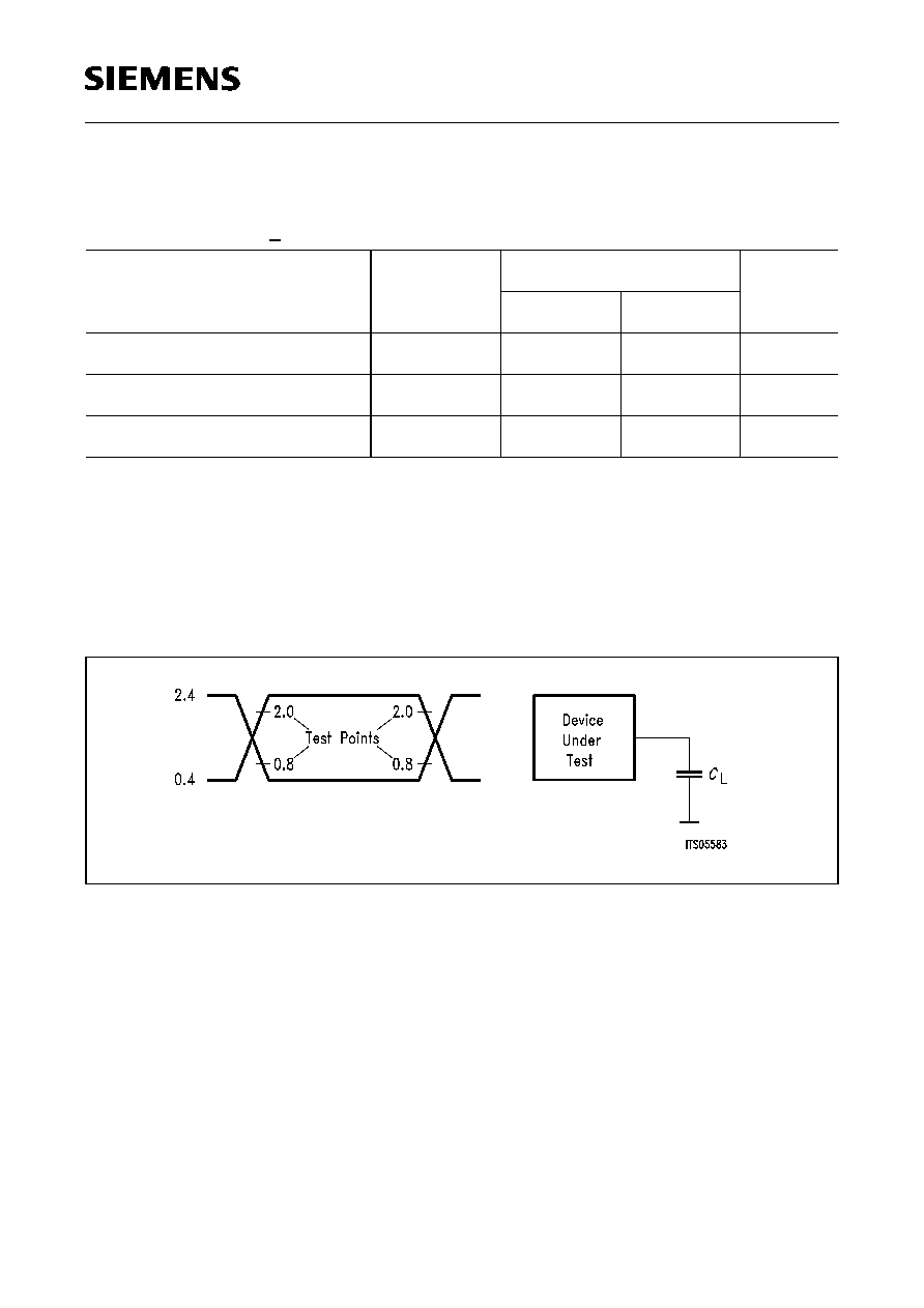
Inputs are driven at 2.4 V for a logical 1 and at 0.4 V for a logical 0. Timing measurements
are made at 2.0 V for a logical 1 and at 0.8 V for a logical 0. The AC testing input/output
waveforms are shown below. Timing values are guaranteed for capacitive loading of
C
L
= 60 pF on all outputs except pins D(7:0), which are specified for
C
L
= 100 pF.
Figure 14
I/O Waveform for AC Tests
Table 18
Capacitances
T
A
= 25 ∞C,
V
DD
= 5 V + 5 %,
V
SS
= 0 V
Parameter
Symbol
Limit Values
Unit
min.
max.
Input capacitance
C
IN
5
pF
Output capacitance
C
OUT
10
pF
I/O capacitance
C
IO
15
pF
PEB 2447
Electrical Characteristics
Semiconductor Group
46
03.97
Figure 15
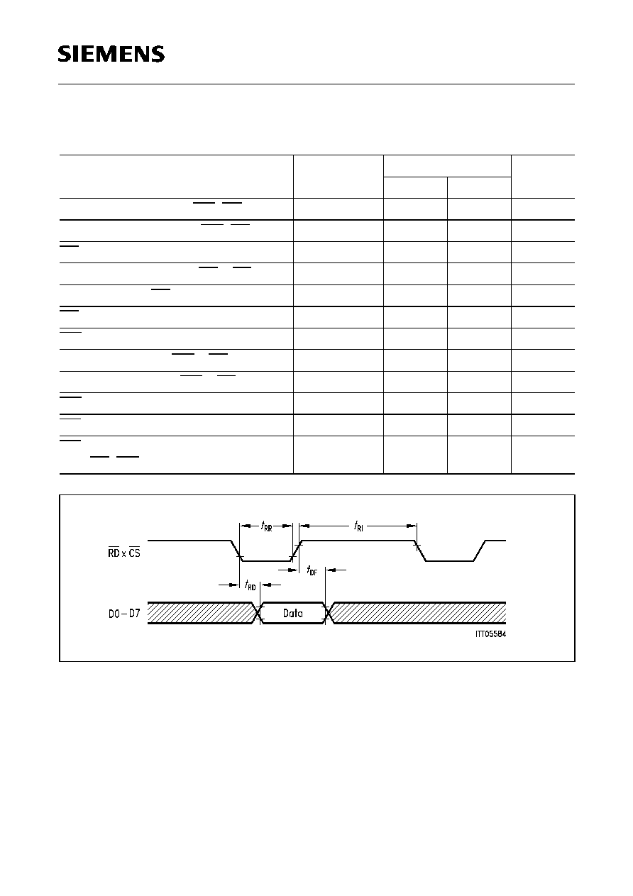
µ
P Read Cycle
Table 19
µ
P Interface Timing Parameters
Parameter
Symbol
Limit Values
Unit
min.
max.
Address setup time to WR, RD
t
AS
10
ns
Address hold time from WR, RD
t
AH
0
ns
RD pulse width
t
RR
120
ns
Data output delay from RD
◊
CS
t
RD
100
ns
Data float from RD
t
DF
25
ns
RD control interval
t
RI
70
ns
WR pulse width
t
WW
60
ns
Data setup time to WR
◊
CS
t
DW
30
ns
Data hold time from WR
◊
CS
t
WD
10
ns
WR control interval
t
WI
70
ns
INT activation delay
t
ID
100
ns
INT activation/deactivation delay
from RD, WR
t
IID
120
ns

PEB 2447
Electrical Characteristics
Semiconductor Group
47
03.97
Figure 16
µ
P Write Cycle
Figure 17
Demultiplexed Address Timing
Figure 18
Interrupt Timing
PEB 2447
Electrical Characteristics
Semiconductor Group
48
03.97
Table 20
PCM Interface Characteristics
Parameter
Symbol
Limit Values
Unit
Condition
min.
max.
Clock period
Clock period low
Clock period high
t
CP
t
CPL
t
CPH
60
27
27
ns
ns
ns
Frame setup time
Frame hold time
t
FS
t
FH
7
20
ns
ns
Serial data input setup time
Serial data input hold time
t
S
t
H
9
20
ns
ns
PCM serial data output delay time
t
D
50
ns
PEB 2447
Electrical Characteristics
Semiconductor Group
49
03.97
Figure 19
AC Characteristics at the PCM Interface
PEB 2447
Electrical Characteristics
Semiconductor Group
50
03.97
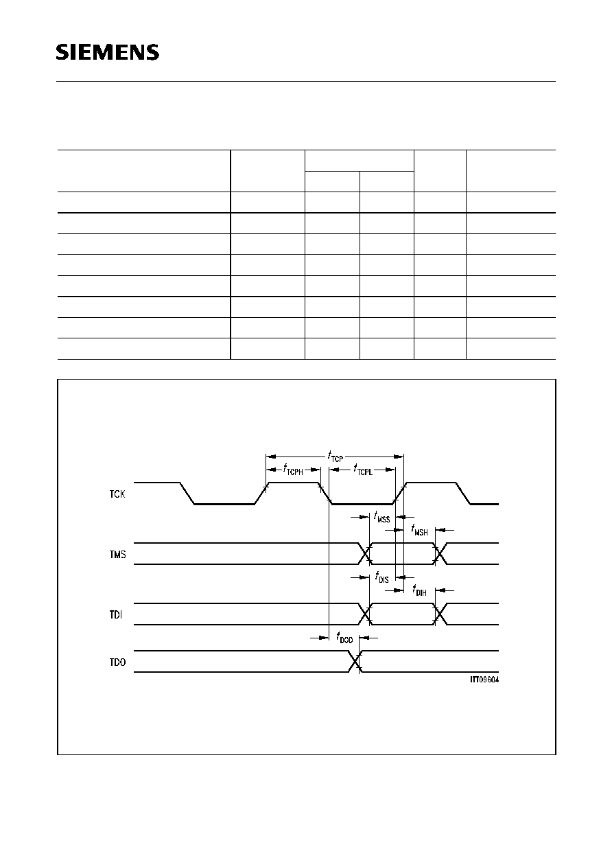
Figure 20
AC Characteristics at Boundary Scan Interface
Table 21
Boundary Scan Timing
Parameter
Symbol
Limit Values
Unit
Condition
min.
max.
Test clock period
t
TCP
160
ns
Test clock period low
t
TCPL
80
ns
Test clock period high
t
TCPH
80
ns
TMS setup time to TCK
t
MSS
30
ns
TMS hold time from TCK
t
MSH
30
ns
TDI setup time to TCK
t
DIS
30
ns
TDI hold time from TCK
t
DIH
30
ns
TDO delay from TCK
t
DOD
60
ns
PEB 2447
Package Outlines
Semiconductor Group
51
03.97
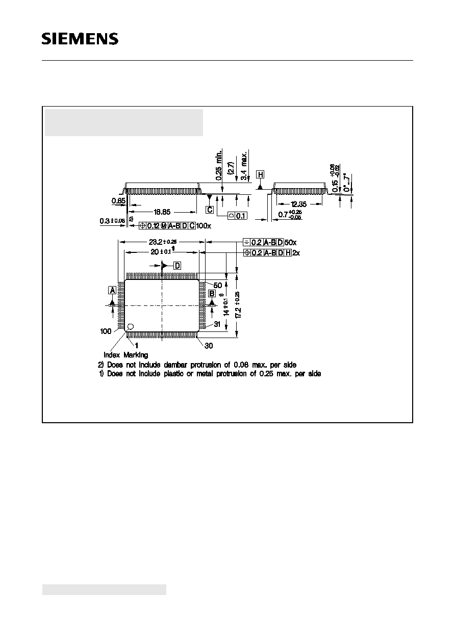
6
Package Outlines
P-MQFP-100-2
(Plastic Metric Quad Flat Package)
G
P
R
0
536
5
Sorts of Packing
Package outlines for tubes, trays etc. are contained in our
Data Book "Package Information".
Dimensions in mm
SMD = Surface Mounted Device