
Data Sheet 10.97
Microcomputer Components
C517A
8-Bit CMOS Microcontroller

C517A Data Sheet
Revision History:
Current Version: 10.97
Previous Version:
none
Page
(in previous
Version)
Page
(in current
Version)
Subjects (major changes since last revision)
Edition 10.97
Published by Siemens AG,
Bereich Halbleiter, Marketing-
Kommunikation, Balanstraþe 73,
81541 M¸nchen
©
Siemens AG 1997.
All Rights Reserved.
Attention please!
As far as patents or other rights of third parties are concerned, liability is only assumed for components, not for applications, processes
and circuits implemented within components or assemblies.
The information describes the type of component and shall not be considered as assured characteristics.
Terms of delivery and rights to change design reserved.
For questions on technology, delivery and prices please contact the Semiconductor Group Offices in Germany or the Siemens Companies
and Representatives worldwide (see address list).
Due to technical requirements components may contain dangerous substances. For information on the types in question please contact
your nearest Siemens Office, Semiconductor Group.
Siemens AG is an approved CECC manufacturer.
Packing
Please use the recycling operators known to you. We can also help you ≠ get in touch with your nearest sales office. By agreement we
will take packing material back, if it is sorted. You must bear the costs of transport.
For packing material that is returned to us unsorted or which we are not obliged to accept, we shall have to invoice you for any costs in-
curred.
Components used in life-support devices or systems must be expressly authorized for such purpose!
Critical components
1
of the Semiconductor Group of Siemens AG, may only be used in life-support devices or systems
2
with the express
written approval of the Semiconductor Group of Siemens AG.
1 A critical component is a component used in a life-support device or system whose failure can reasonably be expected to cause the
failure of that life-support device or system, or to affect its safety or effectiveness of that device or system.
2 Life support devices or systems are intended (a) to be implanted in the human body, or (b) to support and/or maintain and sustain hu-
man life. If they fail, it is reasonable to assume that the health of the user may be endangered.
Semiconductor Group
3
1997-10-01
8-Bit CMOS Microcontroller
Advance Information
C517A
∑
Full upward compatibility with SAB 80C517A/83C517A-5
∑
Up to 24 MHz external operating frequency
≠ 500 ns instruction cycle at 24 MHz operation
∑
Superset of the 8051 architecture with 8 datapointers
∑
On-chip emulation support logic (Enhanced Hooks Technology
TM
)
∑
32K byte on-chip ROM (with optional ROM protection)
≠ alternatively up to 64K byte external program memory
∑
Up to 64K byte external data memory
∑
256 byte on-chip RAM
∑
Additional 2K byte on-chip RAM (XRAM)
∑
Seven 8-bit parallel I/O ports
∑
Two input ports for analog/digital input
(further features are on next page)
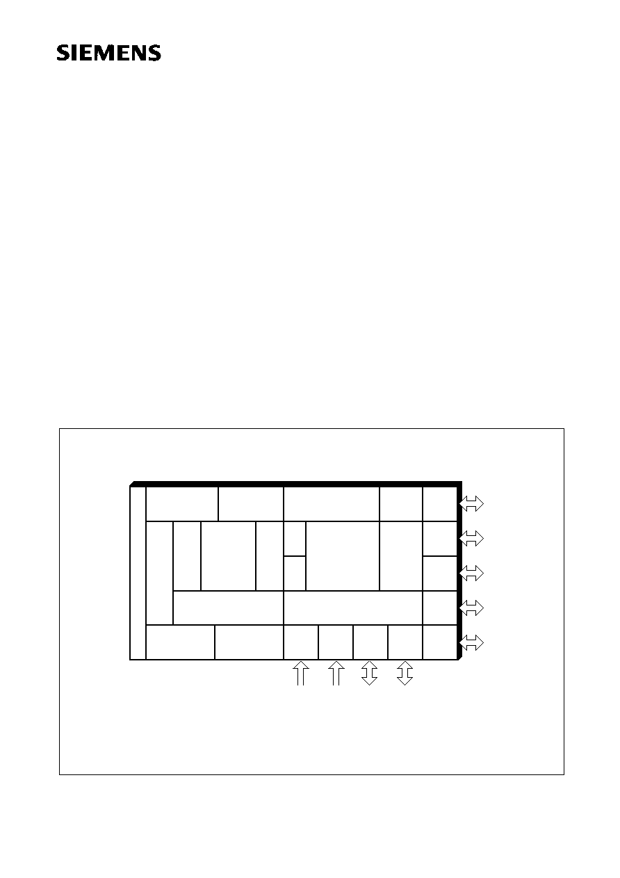
Figure 1
C517A Functional Units
MCA03317
Port 0
Port 1
Port 2
XRAM
RAM
T0
T1
MDU
ROM
I/O
(8 Datapointer)
I/O
Analog/
Digital
Input
Port 3
32k x 8
CPU
Port 8
Input
Digital
Analog/
256 x 8
2K x 8
Port 7
Port 6
Port 5
Port 4
Watchdog
Timer
Oscillator
Watchdog
10-Bit
A/D Converter
8 Bit
USART
UART
8 Bit
Timer
Compare
T2
CCU
Power
Saving
Modes
On-Chip Emulation Support Module
I/O
I/O
I/O
I/O
I/O
C517A
Semiconductor Group
4
1997-10-01
Features (cont'd):
∑
Two full duplex serial interfaces (USART)
≠ 4 operating modes, fixed or variable baud rates
≠ programmable baud rate generators
∑
Four 16-bit timer/counters
≠ Timer 0 / 1 (C501 compatible)
≠ Timer 2 for 16-bit reload, compare, or capture functions
≠ Compare timer for compare/capture functions
∑
Powerful 16-bit compare/capture unit (CCU) with up to 21 high-speed or PWM output channels
and 5 capture inputs
∑
10-bit A/D converter
≠ 12 multiplexed analog inputs
≠ Built-in self calibration
∑
Extended watchdog facilities
≠ 15-bit programmable watchdog timer
≠ Oscillator watchdog
∑
Power saving modes
≠ Slow down mode
≠ Idle mode (can be combined with slow down mode)
≠ Software power-down mode
≠ Hardware power-down mode
∑
17 interrupt sources (7 external, 10 internal) selectable at 4 priority levels
∑
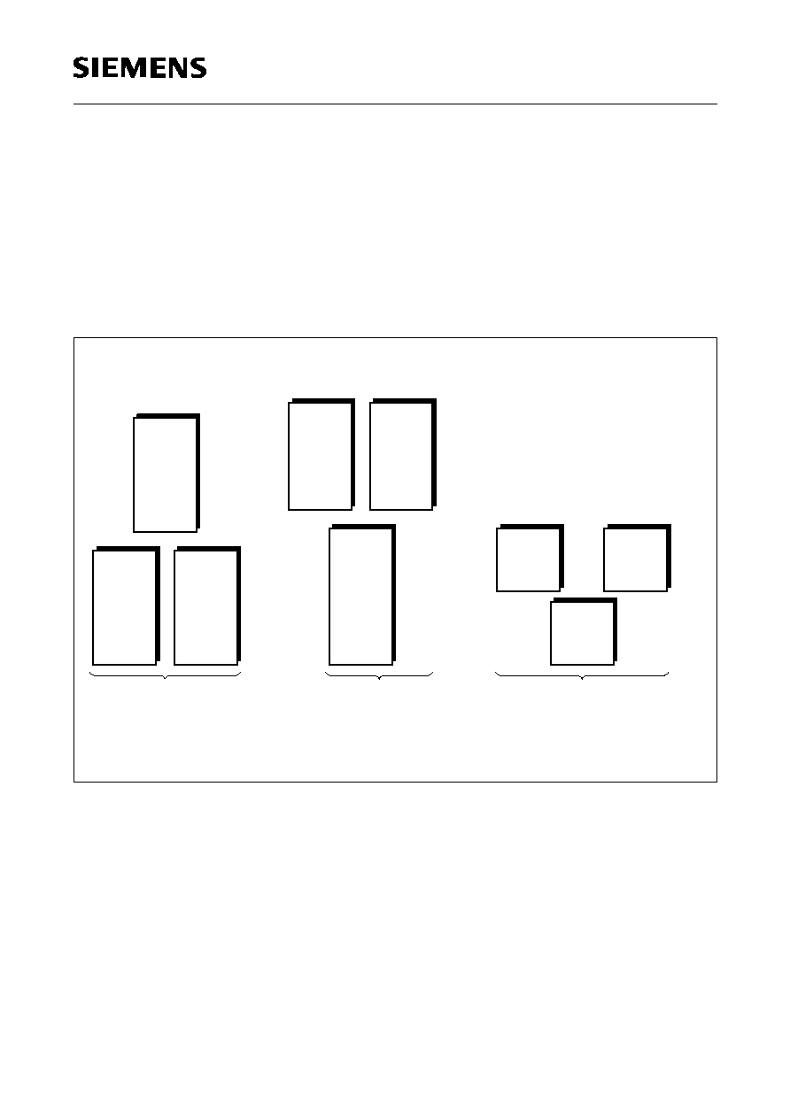
P-MQFP-100 packages
∑
Temperature Ranges:
SAB-C517A
T
A
= 0 to 70
∞
C
SAF-C517A
T
A
= -40 to 85
∞
C
SAH-C517A
T
A
= -40 to 110
∞
C
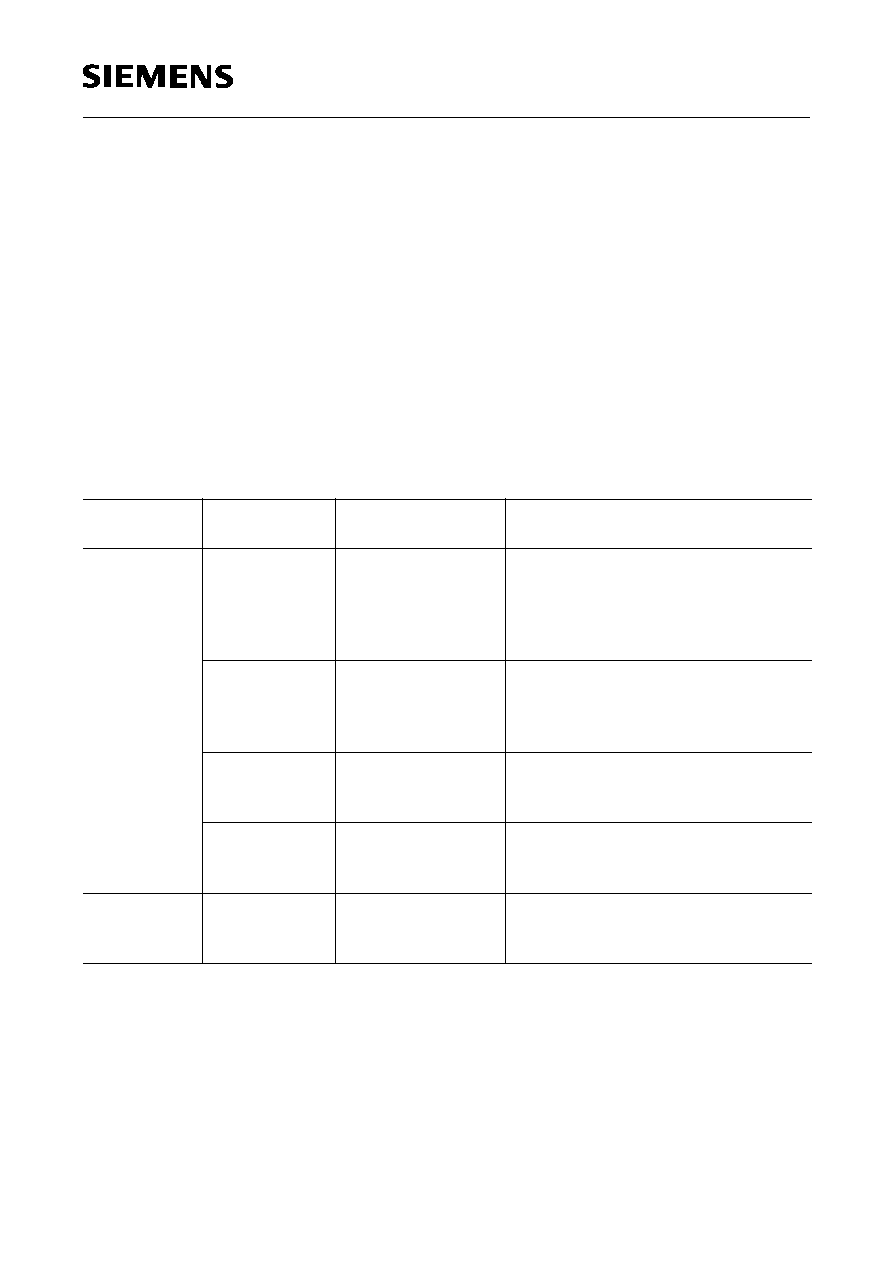
Table 1
Ordering Information
Type
Ordering Code
Package
Description
(8-Bit CMOS microcontroller)
SAB-C517A-4RM
Q67120-DXXXX
P-MQFP-100-2 with mask programmable ROM
(18 MHz)
SAF-C517A-4RM
Q67120-DXXXX
P-MQFP-100-2 with mask programmable ROM
(18 MHz) ext. temp. ≠ 40
∞
C to 85
∞
C
SAB-C517A-4R24M Q67120-DXXXX
P-MQFP-100-2 with mask programmable ROM
(24 MHz)
SAF-C517A-4R24M Q67120-DXXXX
P-MQFP-100-2 with mask programmable ROM
(24 MHz) ext. temp. ≠ 40
∞
C to 85
∞
C
SAB-C517A-LM
Q67127-C1071
P-MQFP-100-2 for external memory (18 MHz)
SAF-C517A-LM
Q67127-C1063
P-MQFP-100-2 for external memory (18 MHz)
ext. temp. ≠ 40
∞
C to 85
∞
C
SAB-C517A-L24M
Q67127-C1072
P-MQFP-100-2 for external memory (24 MHz)
Semiconductor Group
5
1997-10-01
C517A
Note: Versions for extended temperature ranges ≠ 40
∞
C to 110
∞
C (SAH-C517A) are available on
request. The ordering number of ROM types (DXXXX extensions) is defined after program
release (verification) of the customer.
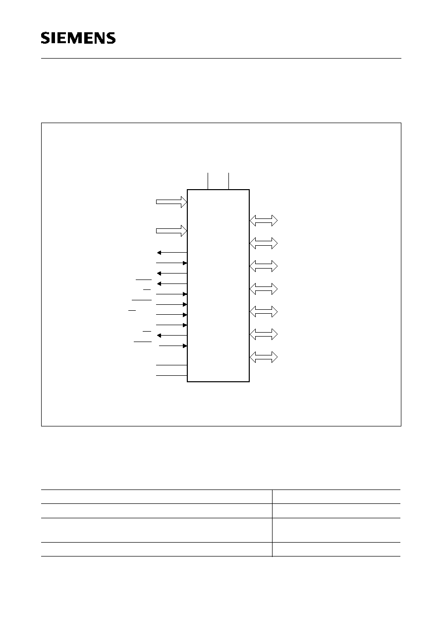
Figure 2
Logic Symbol
Additional Literature
For further information about the C517A the following literature is available:
Title
Ordering Number
C517A 8-Bit CMOS Microcontroller User's Manual
B158-H7053-X-X-7600
C500 Microcontroller Family
Architecture and Instruction Set User's Manual
B158-H6987-X-X-7600
C500 Microcontroller Family - Pocket Guide
B158-H6986-X-X-7600
Port 0
8-Bit Digital I/O
Port 1
Port 2
Port 3
Port 4
Port 5
Port 6
MCL03318
C517A
8-bit Analog/
Port 7
Port 8
4-bit Analog/
V
AREF
AGND
V
OWE
PE/SWD
RO
RESET
EA
ALE
PSEN
XTAL2
XTAL1
CC
V
V
SS
8-Bit Digital I/O
8-Bit Digital I/O
8-Bit Digital I/O
8-Bit Digital I/O
8-Bit Digital I/O
8-Bit Digital I/O
Digital Input
Digital Input
HWPD
C517A
Semiconductor Group
6
1997-10-01
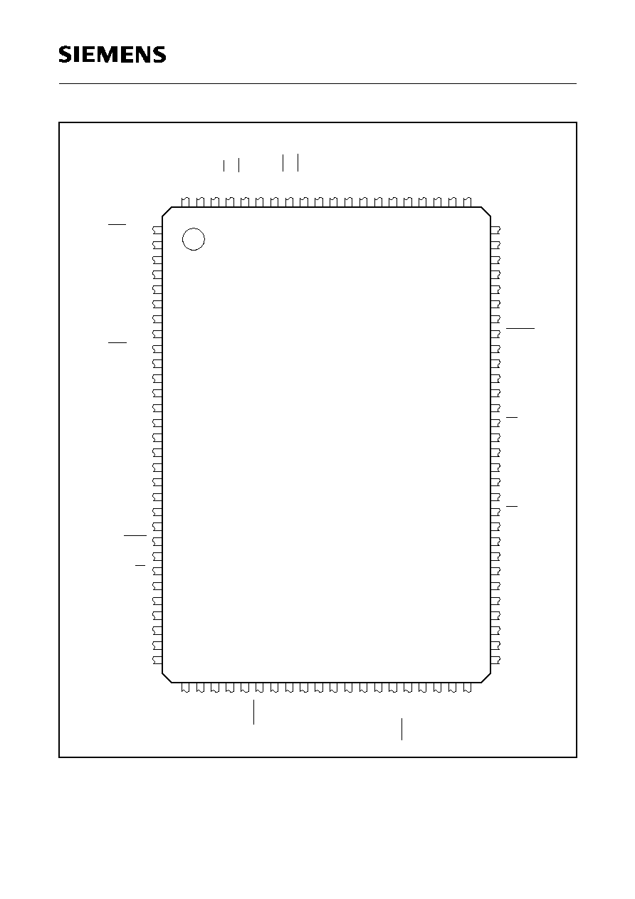
Figure 3
Pin Configuration P-MQFP-100 Package (Top View)
C517A
HWPD
MCP03319
P2.6/A14
P0.3/AD3
P1.5/T2EX
P2.5/A13
P2.4/A12
P2.3/A11
P2.2/A10
P2.1/A9
P2.0/A8
XTAL1
XTAL2
CC1/INT4/P1.1
CC2/INT5/P1.2
N.C.
N.C.
N.C.
N.C.
CC4/INT2/P1.4
P0.4/AD4
P0.5/AD5
P0.6/AD6
P0.7/AD7
CCM7/P5.7
CCM6/P5.6
CCM5/P5.5
CCM1/P5.1
CCM0/P5.0
OWE
ADST/P6.0
RxD1/P6.1
TxD1/P6.2
P6.3
P6.4
P4.0/CM0
P4.1/CM1
P4.2/CM2
PE/SWD
P4.3/CM3
P4.4/CM4
P4.5/CM5
P4.6/CM6
N.C.
N.C.
N.C.
N.C.
P1.6/CLKOUT
P1.7/T2
P3.7/RD
P3.6/WR
P3.5/T1
P3.4/T0
P3.3/INT1
P3.2/INT0
P3.1/TxD0
P3.0/RxD0
N.C.
N.C.
P7.0/AIN0
P7.1/AIN1
P7.2/AIN2
P7.3/AIN3
P7.4/AIN4
P7.5/AIN5
P7.6/AIN6
100
31
80
1
RO
P8.3/AIN11
P8.2/AIN10
P8.1/AIN9
P8.0/AIN8
P6.7
P6.6
P6.5
P2.7/A15
PSEN
ALE
EA
N.C.
P0.0/AD0
P0.1/AD1
N.C.
V
SS
CC
V
V
AGND
AREF
V
SS
V
V
CC
CCM2/P5.2
CCM3/P5.3
CCM4/P5.4
P0.2/AD2
N.C.
CC0/INT3/P1.0
CC3/INT6/P1.3
P7.7/AIN7
RESET
P4.7/CM7
N.C.
N.C.
N.C.
79
2
78
3
77
4
76
5
75
6
74
7
73
8
72
9
71
10
70
11
69
12
68
13
67
14
66
15
65
16
64
17
63
18
62
19
61
20
60
21
59
22
58
23
57
24
56
25
55
26
54
27
53
28
52
29
51
30
99
32
98
33
97
34
96
35
95
36
94
37
93
38
92
39
91
40
90
41
89
42
88
43
87
44
86
45
85
46
84
47
83
48
82
49
81
50
Semiconductor Group
7
1997-10-01
C517A
Table 2
Pin Definitions and Functions
Symbol
Pin Number
I/O*)
Function
P-MQFP-100
P1.0 - P1.7
9 - 6, 1,
100 - 98
9
8
7
6
1
100
99
98
I/O
Port 1
is an 8-bit quasi-bidirectional I/O port with internal pullup
resistors. Port 1 pins that have 1's written to them are
pulled high by the internal pullup resistors, and in that state
can be used as inputs. As inputs, port 1 pins being
externally pulled low will source current (
I
IL
, in the DC
characteristics) because of the internal pullup resistors.
The port is used for the low-order address byte during
program verification. Port 1 also contains the interrupt,
timer, clock, capture and compare pins that are used by
various options. The output latch corresponding to a
secondary function must be programmed to a one (1) for
that function to operate (except when used for the compare
functions). The secondary functions are assigned to the
port 1 pins as follows:
P1.0
INT3 CC0
Interrupt 3 input / compare 0 output /
capture 0 input
P1.1
INT4 CC1
Interrupt 4 input / compare 1 output /
capture 1 input
P1.2
INT5 CC2
Interrupt 5 input / compare 2 output /
capture 2 input
P1.3
INT6 CC3
Interrupt 6 input / compare 3 output /
capture 3 input
P1.4
INT2
Interrupt 2 input
P1.5
T2EX
Timer 2 external reload / trigger input
P1.6
CLKOUT
System clock output
P1.7
T2
Counter 2 input
V
SS
10, 62
≠
Ground (0V)
during normal, idle, and power down operation.
V
CC
11, 63
≠
Supply voltage
during normal, idle, and power down mode.
*) I = Input
O = Output

C517A
Semiconductor Group
8
1997-10-01
XTAL2
12
≠
XTAL2
is the input to the inverting oscillator amplifier and input to
the internal clock generator circuits.
To drive the device from an external clock source, XTAL2
should be driven, while XTAL1 is left unconnected.
Minimum and maximum high and low times as well as rise/
fall times specified in the AC characteristics must be
observed.
XTAL1
13
≠
XTAL1
is the output of the inverting oscillator amplifier. This pin is
used for the oscillator operation with crystal or ceramic
resonator.
P2.0 - P2.7
14 - 21
I/O
Port 2
is an 8-bit quasi-bidirectional I/O port with internal pullup
resistors. Port 2 pins that have 1's written to them are
pulled high by the internal pullup resistors, and in that state
can be used as inputs. As inputs, port 2 pins being
externally pulled low will source current (
I
IL
, in the DC
characteristics) because of the internal pullup resistors.
Port 2 emits the high-order address byte during fetches
from external program memory and during accesses to
external data memory that use 16-bit addresses
(MOVX @DPTR). In this application it uses strong internal
pullup resistors when issuing 1's. During accesses to
external data memory that use 8-bit addresses
(MOVX @Ri), port 2 issues the contents of the P2 special
function register.
PSEN
22
O
The Program Store Enable
output is a control signal that enables the external program
memory to the bus during external fetch operations. It is
activated every six oscillator periods except during
external data memory accesses. The signal remains high
during internal program execution.
ALE
23
O
The Address Latch enable
output is used for latching the address into external
memory during normal operation. It is activated every six
oscillator periods except during an external data memory
access.
*) I = Input
O = Output
Table 2
Pin Definitions and Functions (cont'd)
Symbol
Pin Number
I/O*)
Function
P-MQFP-100
Semiconductor Group
9
1997-10-01
C517A
EA
24
I
External Access Enable
When held high, the C517A executes instructions from the
internal ROM as long as the PC is less than 8000H. When
held low, the C517A fetches all instructions from external
program memory. For the C517A-L this pin must be tied
low.
P0.0 - P0.7
26, 27,
30 - 35
I/O
Port 0
is an 8-bit open-drain bidirectional I/O port. Port 0 pins that
have 1's written to them float, and in that state can be used
as high-impedance inputs. Port 0 is also the multiplexed
low-order address and data bus during accesses to
external program and data memory. In this application it
uses strong internal pullup resistors when issuing 1's. Port
0 also outputs the code bytes during program verification
in the C517A. External pullup resistors are required during
program verification.
HWPD
36
I
Hardware Power Down
A low level on this pin for the duration of one machine cycle
while the oscillator is running resets the C517A. A low level
for a longer period will force the part into hardware power
down mode with the pins floating. There is no internal
pullup resistor connected to this pin.
P5.0 - P5.7
44 - 37
I/O
Port 5
is a quasi-bidirectional I/O port with internal pull-up
resistors. Port 5 pins that have 1 s written to them are
pulled high by the internal pull-up resistors, and in that
state can be used as inputs. As inputs, port 5 pins being
externally pulled low will source current (
I
IL
, in the DC
characteristics) because of the internal pull-up resistors.
This port also serves the alternate function "Concurrent
Compare" and "Set/Reset Compare". The secondary
functions are assigned to the port 5 pins as follows:
CCM0 to CCM7 P5.0 to P5.7:
concurrent compare or Set/Reset lines
*) I = Input
O = Output
Table 2
Pin Definitions and Functions (cont'd)
Symbol
Pin Number
I/O*)
Function
P-MQFP-100
C517A
Semiconductor Group
10
1997-10-01
OWE
45
I
Oscillator Watchdog Enable
A high level on this pin enables the oscillator watchdog.
When left unconnected this pin is pulled high by a weak
internal pull-up resistor. The logic level at OWE should not
be changed during normal operation. When held at low
level the oscillator watchdog function is turned off. During
hardware power down the pullup resistor is switched off.
P6.0 - P6.7
46 - 50,
54 - 56
46
47
48
I/O
Port 6
is a quasi-bidirectional I/O port with internal pull-up
resistors. Port 6 pins that have 1 s written to them are
pulled high by the internal pull-up resistors, and in that
state can be used as inputs. As inputs, port 6 pins being
externally pulled low will source current (
I
IL
, in the
DC characteristics) because of the internal pull-up
resistors.
Port 6 also contains the external A/D converter control pin
and the transmit and receive pins for the serial interface 1.
The output latch corresponding to a secondary function
must be programmed to a one (1) for that function to
operate.
The secondary functions are assigned to the pins of port 6,
as follows:
P6.0
ADST
external A/D converter start pin
P6.1
RxD1
receiver data input of serial interface 1
P6.2
TxD1
transmitter data input of serial interface 1
P8.0 - P8.3
57 - 60
I
Port 8
is a 4-bit unidirectional input port. Port pins can be used for
digital input, if voltage levels meet the specified input high/
low voltages, and for the higher 4-bit of the multiplexed
analog inputs of the A/D converter, simultaneously.
P8.0 - P8.3
AIN8 - AIN11
analog input 8 - 14
RO
61
O
Reset Output
This pin outputs the internally synchronized reset request
signal. This signal may be generated by an external
hardware reset, a watchdog timer reset or an oscillator
watchdog reset. The RO is active low.
*) I = Input
O = Output
Table 2
Pin Definitions and Functions (cont'd)
Symbol
Pin Number
I/O*)
Function
P-MQFP-100
Semiconductor Group
11
1997-10-01
C517A
P4.0 - P4.7
64 - 66,
68 - 72
I/O
Port 4
is an 8-bit quasi-bidirectional I/O port with internal pull-up
resistors. Port 4 pins that have 1's written to them are
pulled high by the internal pull-up resistors, and in that
state can be used as inputs. As inputs, port 4 pins being
externally pulled low will source current (
I
IL
, in the DC
characteristics) because of the internal pull-up resistors.
PE/SWD
67
I
Power saving mode enable / Start watchdog timer
A low level at this pin allows the software to enter the power
saving modes (idle mode, slow down mode, and power
down mode). In case the low level is also seen during
reset, the watchdog timer function is off on default.
Usage of the software controlled power saving modes is
blocked, when this pin is held at high level. A high level
during reset performs an automatic start of the watchdog
timer immediately after reset.
When left unconnected this pin is pulled high by a weak
internal pull-up resistor. During hardware power down the
pullup resistor is switched off.
RESET
73
I
RESET
A low level on this pin for the duration of two machine
cycles while the oscillator is running resets the C517A. A
small internal pullup resistor permits power-on reset using
only a capacitor connected to V
SS
.
V
AREF
78
≠
Reference voltage for the A/D converter
V
AGND
79
≠
Reference ground for the A/D converter
P7.0 - P7.7
87 - 80
Port 7
is an 8-bit unidirectional input port. Port pins can be used
for digital input, if voltage levels meet the specified input
high/low voltages, and for the lower 8-bit of the multiplexed
analog inputs of the A/D converter, simultaneously.
P7.0 - P7.7
AIN0 - AIN7
analog input 8 - 14
*) I = Input
O = Output
Table 2
Pin Definitions and Functions (cont'd)
Symbol
Pin Number
I/O*)
Function
P-MQFP-100
C517A
Semiconductor Group
12
1997-10-01
P3.0 - P3.7
90 - 97
90
91
92
93
94
95
96
97
I/O
Port 3
is an 8-bit quasi-bidirectional I/O port with internal pullup
resistors. Port 3 pins that have 1's written to them are
pulled high by the internal pullup resistors, and in that state
can be used as inputs. As inputs, port 3 pins being
externally pulled low will source current (
I
IL
, in the DC
characteristics) because of the internal pullup resistors.
Port 3 also contains the interrupt, timer, serial port and
external memory strobe pins that are used by various
options. The output latch corresponding to a secondary
function must be programmed to a one (1) for that function
to operate. The secondary functions are assigned to the
pins of port 3, as follows:
P3.0
RxD0
Receiver data input (asynch.) or data
input/output (synch.)of serial interface 0
P3.1
TxD0
Transmitter data output (asynch.) or
clock output (synch.) of serial interface 0
P3.2
INT0
External interrupt 0 input /
timer 0 gate control input
P3.3
INT1
External interrupt 1 input /
timer 1 gate control input
P3.4
T0
Timer 0 counter input
P3.5
T1
Timer 1 counter input
P3.6
WR
WR control output; latches the data byte
from port 0 into the external data
memory
P3.7
RD
RD control output; enables the external
data memory
N.C.
2 - 5, 25,
28, 29, 32,
43, 44,
51 - 53,
74 - 77
88, 89
≠
Not connected
These pins of the P-MQFP-100 package need not be
connected.
*) I = Input
O = Output
Table 2
Pin Definitions and Functions (cont'd)
Symbol
Pin Number
I/O*)
Function
P-MQFP-100

Semiconductor Group
13
1997-10-01
C517A
Figure 4
Block Diagram of the C517A
Port 8
Port 8
Port 7
Port 7
Port 6
Port 6
Port 5
Port 5
Port 4
Port 4
Port 3
Port 3
Port 2
Port 2
Port 1
Port 1
8-Bit Digital I/O
Port 0
Port 0
Programmable
Watchdog Timer
OSC & Timing
Oscillator Watchdog
Serial Channel 1
Baud Rate Generator
Programmable
Serial Channel 0
Timer 1
Timer 0
Timer 2
Compare Timer
Capture
Compare Unit
S & H
Analog
RESET
RO
ALE
EA
PE/SWD
AREF
V
V
AGND
MCB03320
XTAL1
XTAL2
Interrupt Unit
A/D Converter
10 Bit
Emulation
Support
Logic
ROM
32k x 8
2k x 8
XRAM
RAM
256 x 8
CPU
8 Datapointer
Programmable
Baud Rate Generator
MUX
PSEN
HWPD
OWE
C517A
8-Bit Digital I/O
8-Bit Digital I/O
8-Bit Digital I/O
8-Bit Digital I/O
8-Bit Digital I/O
8-Bit Digital I/O
8-Bit Analog/
Digital Input
4-Bit Analog/
Digital Input
C517A
Semiconductor Group
14
1997-10-01
CPU
The C517A is efficient both as a controller and as an arithmetic processor. It has extensive facilities
for binary and BCD arithmetic and excels in its bit-handling capabilities. Efficient use of program
memory results from an instruction set consisting of 44 % one-byte, 41 % two-byte, and 15%
three-byte instructions. With a 12 MHz crystal, 58% of the instructions are executed in 1
µ
s
(
24 MHz:
500 ns).
Special Function Register PSW (Address D0H)
Reset Value : 00H
Bit
Function
CY
Carry Flag
Used by arithmetic instruction.
AC
Auxiliary Carry Flag
Used by instructions which execute BCD operations.
F0
General Purpose Flag
RS1
RS0
Register Bank select control bits
These bits are used to select one of the four register banks.
OV
Overflow Flag
Used by arithmetic instruction.
F1
General Purpose Flag
P
Parity Flag
Set/cleared by hardware after each instruction to indicate an odd/even
number of "one" bits in the accumulator, i.e. even parity.
CY
AC
F0
RS1
RS0
OV
F1
P
D0H
PSW
D7H
D6H
D5H
D4H
D3H
D2H
D1H
D0H
Bit No.
MSB
LSB
RS1
RS0
Function
0
0
Bank 0 selected, data address 00H-07H
0
1
Bank 1 selected, data address 08H-0FH
1
0
Bank 2 selected, data address 10H-17H
1
1
Bank 3 selected, data address 18H-1FH
Semiconductor Group
15
1997-10-01
C517A
Memory Organization
The C517A CPU manipulates operands in the following five address spaces:
≠ up to 64 Kbyte of program memory (32K on-chip program memory for C517A-4R)
≠ up to 64 Kbyte of external data memory
≠ 256 bytes of internal data memory
≠ 2K bytes of internal XRAM data memory
≠ a 128 byte special function register area
Figure 5 illustrates the memory address spaces of the C517A.
Figure 5
C517A Memory Map
ext.
FFFF
8000
0000
7FFF
ext.
(EA = 0)
(EA = 1)
int.
"Code Space"
int.
(XMAP0 = 0)
(XMAP0 = 1)
ext.
FFFF
F800
0000
F7FF
ext.
"Data Space"
"Internal Data Space"
Internal
7F
00
Internal
80
FF
Function
MCB03321
H
H
H
H
H
H
H
H
H
H
H
H
RAM
RAM
Regs.
Special
Indirect
Address
Address
Direct
H
80
FF H

C517A
Semiconductor Group
16
1997-10-01
Reset and System Clock
The reset input is an active low input at pin RESET. Since the reset is synchronized internally, the
RESET pin must be held low for at least two machine cycles (24 oscillator periods) while the
oscillator is running. A pullup resistor is internally connected to
V
CC
to allow a power-up reset with
an external capacitor only. An automatic reset can be obtained when
V
CC
is applied by connecting
the RESET pin to
V
SS
via a capacitor. Figure 6 shows the possible reset circuitries.
Figure 6
Reset Circuitries
MCS03323
RESET
C517A
b)
a)
c)
+
+
&
RESET
RESET
C517A
C517A

Semiconductor Group
17
1997-10-01
C517A
Figure 7 shows the recommended oscillator circuitries for crystal and external clock operation.
Figure 7
Recommended Oscillator Circuitries
MCS03245
C
C
3.5 - 24
MHz
XTAL1
XTAL2
XTAL2
XTAL1
N.C.
External Oscillator
Signal
Crystal Oscillator Mode
Driving from External Source
Crystal Mode:
C = 20 pF 10 pF
(Incl. Stray Capacitance)
C517A
Semiconductor Group
18
1997-10-01
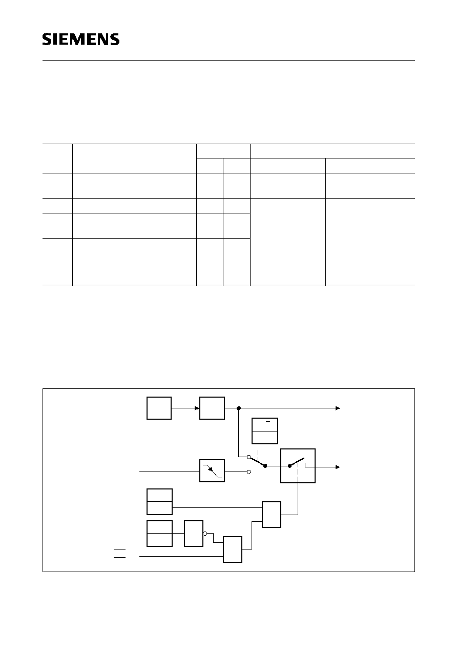
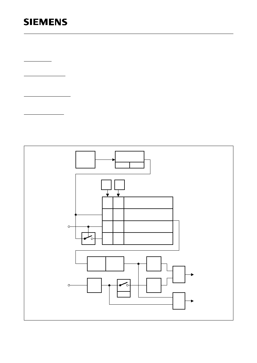
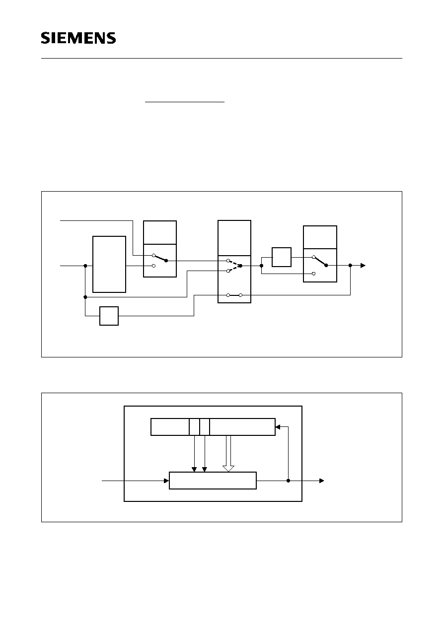
Enhanced Hooks Emulation Concept
The Enhanced Hooks Emulation Concept of the C500 microcontroller family is a new, innovative
way to control the execution of C500 MCUs and to gain extensive information on the internal
operation of the controllers. Emulation of on-chip ROM based programs is possible, too.
Each production chip has built-in logic for the support of the Enhanced Hooks Emulation Concept.
Therefore, no costly bond-out chips are necessary for emulation. This also ensure that emulation
and production chips are identical.
The Enhanced Hooks Technology
TM
1)
, which requires embedded logic in the C500 allows the C500
together with an EH-IC to function similar to a bond-out chip. This simplifies the design and reduces
costs of an ICE-system. ICE-systems using an EH-IC and a compatible C500 are able to emulate
all operating modes of the different versions of the C500 microcontrollers. This includes emulation
of ROM, ROM with code rollover and ROMless modes of operation. It is also able to operate in
single step mode and to read the SFRs after a break.
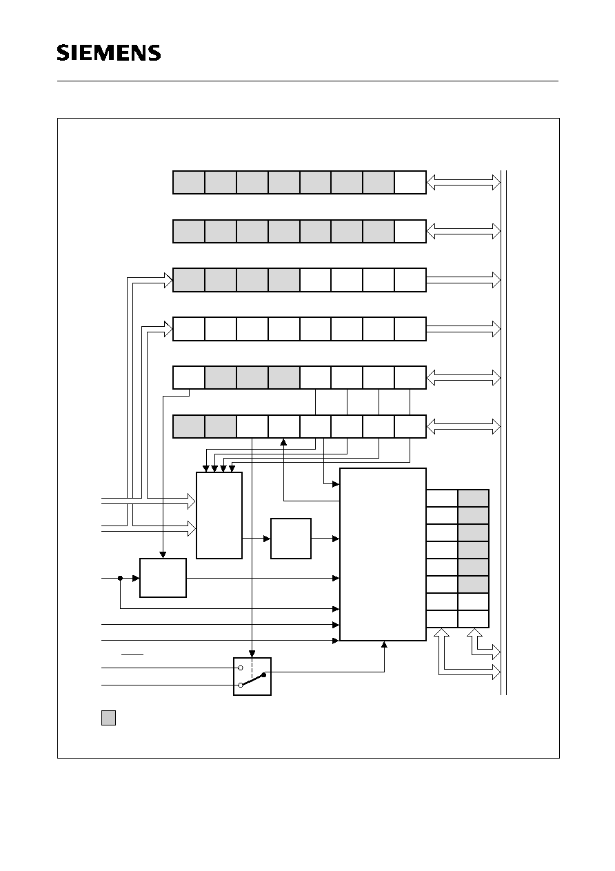
Figure 8
Basic C500 MCU Enhanced Hooks Concept Configuration
Port 0, port 2 and some of the control lines of the C500 based MCU are used by Enhanced Hooks
Emulation Concept to control the operation of the device during emulation and to transfer
informations about the program execution and data transfer between the external emulation
hardware (ICE-system) and the C500 MCU.
1 "Enhanced Hooks Technology" is a trademark and patent of Metalink Corporation licensed to Siemens.
SYSCON
PCON
TCON
RESET
EA
ALE
PSEN
Port 0
Port 2
Port 1
Port 3
opt.
I/O Ports
C500
MCU
2
RPCON
RTCON
Enhanced Hooks
Interface Circuit
RSYSCON
0
RPORT RPORT
TEA TALE TPSEN
EH-IC
ICE-System interface
to emulation hardware
Target System Interface
MCS03254

Semiconductor Group
19
1997-10-01
C517A
Special Function Registers
The registers, except the program counter and the four general purpose register banks, reside in
the special function register area.
The 94 special function registers (SFRs) in the standard and mapped SFR area include pointers
and registers that provide an interface between the CPU and the other on-chip peripherals. All
SFRs with addresses where address bits 0-2 are 0 (e.g. 80H, 88H, 90H, 98H, ..., F8H, FFH) are
bitaddressable. The SFRs of the C517A are listed in table 3 and table 4. In table 3 they are
organized in groups which refer to the functional blocks of the C517A. Table 4 illustrates the
contents of the SFRs in numeric order of their addresses.

C517A
Semiconductor Group
20
1997-10-01
Table 3
Special Function Registers - Functional Blocks
Block
Symbol
Name
Address
Contents after
Reset
CPU
ACC
B
DPH
DPL
DPSEL
PSW
SP
Accumulator
B-Register
Data Pointer, High Byte
Data Pointer, Low Byte
Data Pointer Select Register
Program Status Word Register
Stack Pointer
E0H
1)
F0H
1)
83H
82H
92H
D0H
1)
81H
00H
00H
00H
00H
XXXX X000B
3)
00H
07H
A/D-
Converter
ADCON0
2)
ADCON1
ADDATH
ADDATL
A/D Converter Control Register 0
A/D Converter Control Register 1
A/D Converter Data Register, High Byte
A/D Converter Data Register, Low Byte
D8H
1)
DCH
D9H
DAH
00H
0XXX 0000B
3)
00H
00XX XXXXB
3
Interrupt
System
IEN0
2)
IEN1
2)
IEN2
IP0
2)
IP1
IRCON0
2)
IRCON1
TCON
2)
T2CON
2)
S0CON
2)
CTCON
2)
Interrupt Enable Register 0
Interrupt Enable Register 1
Interrupt Enable Register 2
Interrupt Priority Register 0
Interrupt Priority Register 1
Interrupt Request Control Register 0
Interrupt Request Control Register 1
Timer 0/1 Control Register
Timer 2 Control Register
Serial Channel 0 Control Register
Compare Timer Control Register
A8H
1)
B8H
1)
9AH
A9H
B9H
C0H
1)
D1H
88H
1)
C8H
1)
98H
1)
E1H
00H
00H
XX00 00X0B
3)
00H
XX00 0000B
3)
00H
00H
00H
00H
00H
0X00 0000B
3)
MUL/DIV
Unit
ARCON
MD0
MD1
MD2
MD3
MD4
MD5
Arithmetic Control Register
Multiplication/Division Register 0
Multiplication/Division Register 1
Multiplication/Division Register 2
Multiplication/Division Register 3
Multiplication/Division Register 4
Multiplication/Division Register 5
EFH
E9H
EAH
EBH
ECH
EDH
EEH
0XXXXXXXB
3)
XXH
3)
XXH
3)
XXH
3)
XXH
3)
XXH
3)
XXH
3)
Timer 0 /
Timer 1
TCON
2)
TH0
TH1
TL0
TL1
TMOD
Timer 0/1 Control Register
Timer 0, High Byte
Timer 1, High Byte
Timer 0, Low Byte
Timer 1, Low Byte
Timer Mode Register
88H
1)
8CH
8DH
8AH
8BH
89H
00H
00H
00H
00H
00H
00H
1) Bit-addressable special function registers
2) This special function register is listed repeatedly since some bits of it also belong to other functional blocks.
3) `X' means that the value is undefined and the location is reserved
Semiconductor Group
21
1997-10-01
C517A
Compare/
Capture
Unit
(CCU)
Timer 2
CCEN
CC4EN
CCH1
CCH2
CCH3
CCH4
CCL1
CCL2
CCL3
CCL4
CMEN
CMH0
CMH1
CMH2
CMH3
CMH4
CMH5
CMH6
CMH7
CML0
CML1
CML2
CML3
CML4
CML5
CML6
CML7
CMSEL
CRCH
CRCL
COMSETL
COMSETH
COMCLRL
COMCLRH
SETMSK
CLRMSK
CTCON
2)
CTRELH
CTRELL
TH2
TL2
T2CON
2)
IRCON0
2)
Compare/Capture Enable Register
Compare/Capture 4 Enable Register
Compare/Capture Register 1, High Byte
Compare/Capture Register 2, High Byte
Compare/Capture Register 3, High Byte
Compare/Capture Register 4, High Byte
Compare/Capture Register 1, Low Byte
Compare/Capture Register 2, Low Byte
Compare/Capture Register 3, Low Byte
Compare/Capture Register 4, Low Byte
Compare Enable Register
Compare Register 0, High Byte
Compare Register 1, High Byte
Compare Register 2, High Byte
Compare Register 3, High Byte
Compare Register 4, High Byte
Compare Register 5, High Byte
Compare Register 6, High Byte
Compare Register 7, High Byte
Compare Register 0, Low Byte
Compare Register 1, Low Byte
Compare Register 2, Low Byte
Compare Register 3, Low Byte
Compare Register 4, Low Byte
Compare Register 5, Low Byte
Compare Register 6, Low Byte
Compare Register 7, Low Byte
Compare Input Select
Comp./Rel./Capt. Register High Byte
Comp./Rel./Capt. Register Low Byte
Compare Set Register Low Byte
Compare Set Register, High Byte
Compare Clear Register, Low Byte
Compare Clear Register, High Byte
Compare Set Mask Register
Compare Clear Mask Register
Compare Timer Control Register
Compare Timer Rel. Register, High Byte
Compare Timer Rel. Register, Low Byte
Timer 2, High Byte
Timer 2, Low Byte
Timer 2 Control Register
Interrupt Request Control Register 0
C1H
C9H
C3H
C5H
C7H
CFH
C2H
C4H
C6H
CEH
F6H
D3H
D5H
D7H
E3H
E5H
E7H
F3H
F5H
D2H
D4H
D6H
E2H
E4H
E6H
F2H
F4H
F7H
CBH
CAH
A1H
A2H
A3H
A4H
A5H
A6H
E1H
DFH
DEH
CDH
CCH
C8H
1)
C0H
1)
00H
00H
00H
00H
00H
00H
00H
00H
00H
00H
00H
00H
00H
00H
00H
00H
00H
00H
00H
00H
00H
00H
00H
00H
00H
00H
00H
00H
00H
00H
00H
00H
00H
00H
00H
00H
0X00 0000B
3
)
00H
00H
00H
00H
00H
00H
1) Bit-addressable special function registers
2) This special function register is listed repeatedly since some bits of it also belong to other functional blocks.
3) `X' means that the value is undefined and the location is reserved
Table 3
Special Function Registers - Functional Blocks (cont'd)
Block
Symbol
Name
Address
Contents after
Reset

C517A
Semiconductor Group
22
1997-10-01
Ports
P0
P1
P2
P3
P4
P5
P6
P7
P8
Port 0
Port 1
Port 2
Port 3
Port 4
Port 5
Port 6
Port 7, Analog/Digital Input
Port 8, Analog/Digital Input, 4-bit
80H
1)
90H
1)
A0H
1)
B0H
1)
E8H
1)
F8H
1)
FAH
DBH
DDH
FFH
FFH
FFH
FFH
FFH
FFH
FFH
≠
≠
XRAM
XPAGE
SYSCON
2)
Page Address Register for Extended
On-Chip RAM
System/XRAM Control Register
91H
B1H
00H
XXXX XX01B
3)
Serial
Channels
ADCON0
2)
PCON
2)
S0BUF
S0CON
S0RELL
S0RELH
S1BUF
S1CON
S1RELL
S1RELH
A/D Converter Control Register
Power Control Register
Serial Channel 0 Buffer Register
Serial Channel 0 Control Register
Serial Channel 0 Reload Reg., Low Byte
Serial Channel 0 Reload Reg., High Byte
Serial Channel 1 Buffer Register
Serial Channel 1 Control Register
Serial Channel 1 Reload Reg., Low Byte
Serial Channel 1 Reload Reg., High Byte
D8H
1)
87H
99H
98H
1)
AAH
BAH
9CH
9BH
9DH
BBH
00H
00H
XXH
3
)
00H
D9H
XXXX XX11B
3)
XXH
3
)
0X00 0000B
3)
00H
XXXX XX11B
3)
Watchdog IEN0
2)
IEN1
2)
IP0
2)
WDTREL
Interrupt Enable Register 0
Interrupt Enable Register 1
Interrupt Priority Register 0
Watchdog Timer Reload Register
A8H
1)
B8H
1)
A9H
86H
00H
00H
00H
00H
Pow. Sav.
Modes
PCON
2)
Power Control Register
87H
00H
1) Bit-addressable special function registers
2) This special function register is listed repeatedly since some bits of it also belong to other functional blocks.
3) `X' means that the value is undefined and the location is reserved.
Table 3
Special Function Registers - Functional Blocks (cont'd)
Block
Symbol
Name
Address
Contents after
Reset
Semiconductor Group
23
1997-10-01
C517A
Table 4
Contents of the SFRs, SFRs in numeric order of their addresses
Addr Register
Content
after
Reset
1)
Bit 7
Bit 6
Bit 5
Bit 4
Bit 3
Bit 2
Bit 1
Bit 0
80H
2)
P0
FFH
.7
.6
.5
.4
.3
.2
.1
.0
81H SP
07H
.7
.6
.5
.4
.3
.2
.1
.0
82H DPL
00H
.7
.6
.5
.4
.3
.2
.1
.0
83H DPH
00H
.7
.6
.5
.4
.3
.2
.1
.0
83H WDTREL 00H
WDT-
PSEL
.6
.5
.4
.3
.2
.1
.0
87H PCON
00H
SMOD PDS
IDLS
SD
GF1
GF0
PDE
IDLE
88H
2)
TCON
00H
TF1
TR1
TF0
TR0
IE1
IT1
IE0
IT0
89H TMOD
00H
GATE
C/T
M1
M0
GATE
C/T
M1
M0
8AH TL0
00H
.7
.6
.5
.4
.3
.2
.1
.0
8BH TL1
00H
.7
.6
.5
.4
.3
.2
.1
.0
8CH TH0
00H
.7
.6
.5
.4
.3
.2
.1
.0
8DH TH1
00H
.7
.6
.5
.4
.3
.2
.1
.0
90H
2)
P1
FFH
T2
CLK-
OUT
T2EX
INT2
INT6
INT5
INT4
INT3
91H XPAGE
00H
.7
.6
.5
.4
.3
.2
.1
.0
92H DPSEL
XXXX-
X000B
≠
≠
≠
≠
≠
.2
.1
.0
98H
2)
S0CON
00H
SM0
SM1
SM20
REN0
TB80
RB80
TI0
RI0
99H S0BUF
XXH
.7
.6
.5
.4
.3
.2
.1
.0
9AH IEN2
XX00-
00X0B
≠
≠
ECR
ECS
ECT
ECMP
≠
ES1
9BH S1CON
0X00-
0000B
SM
≠
SM21
REN1
TB81
RB81
TI1
RI1
9CH S1BUF
XXH
.7
.6
.5
.4
.3
.2
.1
.0
9DH S1RELL
00H
.7
.6
.5
.4
.3
.2
.1
.0
A0H
2)
P2
FFH
.7
.6
.5
.4
.3
.2
.1
.0
A1H
COMSETL
00H
.7
.6
.5
.4
.3
.2
.1
.0
A2H
COMSETH
00H
.7
.6
.5
.4
.3
.2
.1
.0
A3H
COMCLRL
00H
.7
.6
.5
.4
.3
.2
.1
.0
1) `X' means that the value is undefined and the location is reserved
2) Shaded registers are bit-addressable special function registers

C517A
Semiconductor Group
24
1997-10-01
A4H
COMCLRH
00H
.7
.6
.5
.4
.3
.2
.1
.0
A5H SETMSK 00H
.7
.6
.5
.4
.3
.2
.1
.0
A6H CLRMSK 00H
.7
.6
.5
.4
.3
.2
.1
.0
A8H
2)
IEN0
00H
EAL
WDT
ET2
ES0
ET1
EX1
ET0
EX0
A9H IP0
00H
OWDS WDTS
.5
.4
.3
.2
.1
.0
AAH S0RELL
D9H
.7
.6
.5
.4
.3
.2
.1
.0
B0H
2)
P3
FFH
RD
WR
T1
T0
INT1
INT0
TxD0
RxD0
B1H SYSCON XXXX-
XX01B
≠
≠
≠
≠
≠
≠
XMAP1 XMAP0
B8H
2)
IEN1
00H
EXEN2 SWDT
EX6
EX5
EX4
EX3
EX2
EADC
B9H IP1
XX00-
0000B
≠
≠
.5
.4
.3
.2
.1
.0
BAH S0RELH XXXX-
XX11B
≠
≠
≠
≠
≠
≠
.1
.0
BBH S1RELH XXXX-
XX11B
≠
≠
≠
≠
≠
≠
.1
.0
C0H
2)
IRCON0
00H
EXF2
TF2
IEX6
IEX5
IEX4
IEX3
IEX2
IADC
C1H CCEN
00H
COCA
H3
COCAL
3
COCA
H2
COCAL
2
COCA
H1
COCAL
1
COCA
H0
COCA
L0
C2H CCL1
00H
.7
.6
.5
.4
.3
.2
.1
.0
C3H CCH1
00H
.7
.6
.5
.4
.3
.2
.1
.0
C4H CCL2
00H
.7
.6
.5
.4
.3
.2
.1
.0
C5H CCH2
00H
.7
.6
.5
.4
.3
.2
.1
.0
C6H CCL3
00H
.7
.6
.5
.4
.3
.2
.1
.0
C7H CCH3
00H
.7
.6
.5
.4
.3
.2
.1
.0
C8H
2)
T2CON
00H
T2PS
I3FR
I2FR
T2R1
T2R0
T2CM
T2I1
T2I0
C9H CC4EN
00H
COCO
EN1
COCO
N2
COCO
N1
COCO
N0
COCO
EN0
COCA
H4
COCA
L4
COMO
1) `X' means that the value is undefined and the location is reserved
2) Shaded registers are bit-addressable special function registers
Table 4
Contents of the SFRs, SFRs in numeric order of their addresses (cont'd)
Addr Register
Content
after
Reset
1)
Bit 7
Bit 6
Bit 5
Bit 4
Bit 3
Bit 2
Bit 1
Bit 0

Semiconductor Group
25
1997-10-01
C517A
CAH CRCL
00H
.7
.6
.5
.4
.3
.2
.1
.0
CBH CRCH
00H
.7
.6
.5
.4
.3
.2
.1
.0
CCH TL2
00H
.7
.6
.5
.4
.3
.2
.1
.0
CDH TH2
00H
.7
.6
.5
.4
.3
.2
.1
.0
CEH CCL4
00H
.7
.6
.5
.4
.3
.2
.1
.0
CFH CCH4
00H
.7
.6
.5
.4
.3
.2
.1
.0
D0H
2)
PSW
00H
CY
AC
F0
RS1
RS0
OV
F1
P
D1H IRCON1 00H
ICMP7 ICMP6 ICMP5 ICMP4 ICMP3 ICMP2 ICMP1 ICMP0
D2H CML0
00H
.7
.6
.5
.4
.3
.2
.1
.0
D3H CMH0
00H
.7
.6
.5
.4
.3
.2
.1
.0
D4H CML1
00H
.7
.6
.5
.4
.3
.2
.1
.0
D5H CMH1
00H
.7
.6
.5
.4
.3
.2
.1
.0
D6H CML2
00H
.7
.6
.5
.4
.3
.2
.1
.0
D7H CMH2
00H
.7
.6
.5
.4
.3
.2
.1
.0
D8H
2)
ADCON0 00H
BD
CLK
ADEX
BSY
ADM
MX2
MX1
MX0
D9H ADDATH 00H
.9
.8
.7
.6
.5
.4
.3
.2
DAH ADDATL 00XX-
XXXXB
.1
.0
≠
≠
≠
≠
≠
≠
DBH P7
≠
.7
.6
.5
.4
.3
.2
.1
.0
DCH ADCON1 0XXX-
0000B
ADCL
≠
≠
≠
MX3
MX2
MX1
MX0
DDH P8
≠
≠
≠
≠
≠
.3
.2
.1
.0
DEH CTRELL 00H
.7
.6
.5
.4
.3
.2
.1
.0
DFH CTRELH 00H
.7
.6
.5
.4
.3
.2
.1
.0
E0H
2)
ACC
00H
.7
.6
.5
.4
.3
.2
.1
.0
E1H CTCON
0X00.
0000B
T2PS1 ≠
ICR
ICS
CTF
CLK2
CLK1
CLK0
E2H CML3
00H
.7
.6
.5
.4
.3
.2
.1
.0
1) `X' means that the value is undefined and the location is reserved
2) Shaded registers are bit-addressable special function registers
Table 4
Contents of the SFRs, SFRs in numeric order of their addresses (cont'd)
Addr Register
Content
after
Reset
1)
Bit 7
Bit 6
Bit 5
Bit 4
Bit 3
Bit 2
Bit 1
Bit 0
C517A
Semiconductor Group
26
1997-10-01
E3H CMH3
00H
.7
.6
.5
.4
.3
.2
.1
.0
E4H CML4
00H
.7
.6
.5
.4
.3
.2
.1
.0
E5H CMH4
00H
.7
.6
.5
.4
.3
.2
.1
.0
E6H CML5
00H
.7
.6
.5
.4
.3
.2
.1
.0
E7H CMH5
00H
.7
.6
.5
.4
.3
.2
.1
.0
E8H
2)
P4
FFH
CM7
CM6
CM5
CM4
CM3
CM2
CM1
CM0
E9H MD0
XXH
.7
.6
.5
.4
.3
.2
.1
.0
EAH MD1
XXH
.7
.6
.5
.4
.3
.2
.1
.0
EBH MD2
XXH
.7
.6
.5
.4
.3
.2
.1
.0
ECH MD3
XXH
.7
.6
.5
.4
.3
.2
.1
.0
EDH MD4
XXH
.7
.6
.5
.4
.3
.2
.1
.0
EEH MD5
XXH
.7
.6
.5
.4
.3
.2
.1
.0
EFH ARCON
0XXX.
XXXXB
MDEF
MDOV SLR
SC.4
SC.3
SC.2
SC.1
SC.0
F0H
2)
B
00H
.7
.6
.5
.4
.3
.2
.1
.0
F2H CML6
00H
.7
.6
.5
.4
.3
.2
.1
.0
F3H CMH6
00H
.7
.6
.5
.4
.3
.2
.1
.0
F4H CML7
00H
.7
.6
.5
.4
.3
.2
.1
.0
F5H CMH7
00H
.7
.6
.5
.4
.3
.2
.1
.0
F6H CMEN
00H
.7
.6
.5
.4
.3
.2
.1
.0
F7H CMSEL
00H
.7
.6
.5
.4
.3
.2
.1
.0
F8H
2)
P5
FFH
CCM7
CCM6
CCM5
CCM4
CCM3
CCM2
CCM1
CCM0
FAH P6
FFH
.7
.6
.5
.4
.3
TxD1
RxD1
ADST
1) `X' means that the value is undefined and the location is reserved
2) Shaded registers are bit-addressable special function registers
Table 4
Contents of the SFRs, SFRs in numeric order of their addresses (cont'd)
Addr Register
Content
after
Reset
1)
Bit 7
Bit 6
Bit 5
Bit 4
Bit 3
Bit 2
Bit 1
Bit 0

Semiconductor Group
27
1997-10-01
C517A
Digital I/O Ports
The C517A allows for digital I/O on 56 lines grouped into 7 bidirectional 8-bit ports. Each port bit
consists of a latch, an output driver and an input buffer. Read and write accesses to the I/O ports P0
through P6 are performed via their corresponding special function registers P0 to P6.
The output drivers of port 0 and 2 and the input buffers of port 0 are also used for accessing external
memory. In this application, port 0 outputs the low byte of the external memory address, time-
multiplexed with the byte being written or read. Port 2 outputs the high byte of the external memory
address when the address is 16 bits wide. Otherwise, the port 2 pins continue emitting the P2 SFR
contents.
Analog Input Ports
Ports 7 (8-bit) an 8 (4-bit) are input ports only and provide two functions. When used as digital
inputs, the corresponding SFR P7 and P8 contains the digital value applied to the port 7/8 lines.
When used for analog inputs the desired analog channel is selected by a four-bit field in SFR
ADCON1. Of course, it makes no sense to output a value to these input-only ports by writing to the
SFR P7 or P8. This will have no effect.
If a digital value is to be read, the voltage levels are to be held within the input voltage specifications
(
V
IL
/
V
IH
). Since P7 and P8 are not bit-addressable, all input lines of P7 and P8 are read at the same
time by byte instructions.
Nevertheless, it is possible to use port 7 and 8 simultaneously for analog and digital input. However,
care must be taken that all bits of P7 and P8 that have an undetermined value caused by their
analog function are masked.
C517A
Semiconductor Group
28
1997-10-01
Timer / Counter 0 and 1
Timer/Counter 0 and 1 can be used in four operating modes as listed in table 5:
In the "timer" function (C/T = `0') the register is incremented every machine cycle. Therefore the
count rate is
f
OSC
/12.
In the "counter" function the register is incremented in response to a 1-to-0 transition at its
corresponding external input pin (P3.4/T0, P3.5/T1). Since it takes two machine cycles to detect a
falling edge the max. count rate is
f
OSC
/24. External inputs INT0 and INT1 (P3.2, P3.3) can be
programmed to function as a gate to facilitate pulse width measurements. Figure 9 illustrates the
input clock logic.
Figure 9
Timer/Counter 0 and 1 Input Clock Logic
Table 5
Timer/Counter 0 and 1 Operating Modes
Mode
Description
TMOD
Input Clock
M1
M0
internal
external (max)
0
8-bit timer/counter with a
divide-by-32 prescaler
0
0
f
OSC
/12x32
f
OSC
/24x32
1
16-bit timer/counter
1
1
f
OSC
/12
f
OSC
/24
2
8-bit timer/counter with
8-bit autoreload
1
0
3
Timer/counter 0 used as one
8-bit timer/counter and one
8-bit timer
Timer 1 stops
1
1
12
f
OSC
/12
MCS01768
OSC
f
C/T
TMOD
0
Control
Timer 0/1
Input Clock
TCON
TR 0/1
Gate
TMOD
&
=1
1
P3.4/T0
P3.5/T1
max
P3.2/INT0
P3.3/INT1
OSC
/24
f
1
˜
_
<

Semiconductor Group
29
1997-10-01
C517A
Compare / Capture Unit (CCU)
The compare/capture unit is one of the C517A's most powerful peripheral units for use in all kinds
of digital signal generation and event capturing like pulse generation, pulse width modulation, pulse
width measuring etc. The CCU consists of two 16-bit timer/counters with automatic reload feature
and an array of 13 compare or compare/capture registers. A set of six control registers is used for
flexible adapting of the CCU to a wide variety of user's applications.
The block diagram in figure 10 shows the general configuration of the CCU. All CC1 to CC4
registers and the CRC register are exclusively assigned to timer 2. Each of the eight compare
registers CM0 through CM7 can either be assigned to timer 2 or to the faster compare timer, e.g. to
provide up to 8 PWM output channels. The assignment of the CMx registers - which can be done
individually for every single register - is combined with an automatic selection of one of the two
possible compare modes.
Figure 10
Timer 2 Block Diagram
Capt./Comp.
MCB01577
Max.Clock =
f
OSC
Timer 2
(CM7)
16-bit
Compare
(CM0)
8x
Compare Timer
Prescaler
(CTREL)
16-bit Reload
Comp.
4 (CC4)
Capt./Comp. 3 (CC3)
Capt./Comp. 2 (CC2)
Capt./Comp. 1 (CC1)
16-bit Rel.Capt. (CRC)
"Internal Bus"
Shadow
Latch
CC4EN
Logik
Control
Port
Latch
P1-
I/O-
I/O-
P5-
Latch
/12
Max.Clock =
/2
OSC
f
Prescaler
Latch
I/O-
P4-
Logik
Port
Control
C517A
Semiconductor Group
30
1997-10-01
The main functional blocks of the CCU are:
≠ Timer 2 with
f
OSC
/12 input clock, 2-bit prescaler, 16-bit reload, counter/gated timer mode and
overflow interrupt request.
≠ Compare timer with
f
OSC
/2 input clock, 3-bit prescaler, 16-bit reload and overflow interrupt
request.
≠ Compare/(reload/) capture register array consisting of four different kinds of registers:
one 16-bit compare/reload/capture register,
three 16-bit compare/capture registers,
one 16-bit compare/capture register with additional "concurrent compare" feature,
eight 16-bit compare registers with timer-overflow controlled loading.
Table 6 shows the possible configurations of the CCU and the corresponding compare modes
which can be selected. The following sections describe the function of these configurations.
Table 6
CCU Configurations
Assigned
Timer
Compare
Register
Compare Output at
Possible Modes
Timer 2
CRCH/CRCL
CCH1/CCL1
CCH2/CCL2
CCH3/CCL3
CCH4/CCL4
P1.0/INT3/CC0
P1.1/INT4/CC1
P1.2/INT5/CC2
P1.3/INT6/CC3
P1.4/INT2/CC4
Compare mode 0, 1 + Reload
Compare mode 0, 1 / capture
Compare mode 0, 1 / capture
Compare mode 0, 1 / capture
Compare mode 0, 1 / capture
CCH4/CCL4
P1.4/INT2/CC4
P5.0/CCM0
to
P5.7/CCM7
Compare mode 1
"Concurrent compare"
CMH0/CML0
to
CMH7/CML7
P4.0/CM0
to
P4.7/CM7
Compare mode 0
COMSET
COMCLR
P5.0/CCM0
to
P5.7/CCM7
Compare mode 2
Compare
Timer
CMH0/CML0
to
CMH7/CML7
P4.0/CM0
to
P4.7/CM7
Compare mode 1
Semiconductor Group
31
1997-10-01
C517A
Timer 2 Operation
Timer Mode: In timer function, the count rate is derived from the oscillator frequency. A prescaler
offers the possibility of selecting a count rate of 1/12 or 1/24 of the oscillator frequency.
Gated Timer Mode: In gated timer function, the external input pin P1.7/T2 operates as a gate to the
input of timer 2. If T2 is high, the internal clock input is gated to the timer. T2 = 0 stops the counting
procedure. The external gate signal is sampled once every machine cycle.
Event Counter Mode: In the event counter function. the timer 2 is incremented in response to a
1-to-0 transition at its corresponding external input pin P1.7/T2. In this function, the external input is
sampled every machine cycle. The maximum count rate is 1/24 of the oscillator frequency.
Reload of Timer 2: Two reload modes are selectable:
In mode 0, when timer 2 rolls over from all 1's to all 0's, it not only sets TF2 but also causes the
timer 2 registers to be loaded with the 16-bit value in the CRC register, which is preset by software.
In mode 1, a 16-bit reload from the CRC register is caused by a negative transition at the
corresponding input pin P1.5/T2EX.
Figure 11
Block Diagram of Timer 2
MCB03328
Programmable
OSC
T2PS
T2PS1
No input selected
Timer stop
0
0
0
1
1
0
1
1
Counter function
via ext. input P1.7/T2
Timer function
Gated timer function
by ext. input P1.7/T2
T2I1
T2I0
SFR T2CON
P1.7/T2
TL2
TH2
TF2
EXF2
Interrupt
EXEN2
Sync
P1.5/T2EX
Reload
Timer 2
Input Clock
1
1
(8 Bits)
(8 Bits)
_
<
_
<
Prescaler

C517A
Semiconductor Group
32
1997-10-01
Compare Timer Operation
The compare timer receives its input clock from a programmable prescaler which provides input
frequencies, ranging from
f
OSC
/2 up to
f
OSC
/256. The compare timer is, once started, a free-running
16-bit timer, which on overflow is automatically reloaded by the contents of a 16-bit reload register.
The compare timer has - as any other timer in the C517A - their own interrupt request flags CTF.
These flags are set when the timer count rolls over from all ones to the reload value. Figure 12
shows the block diagram of compare timer and compare timer 1.
Figure 12
Compare Timer Block Diagram
16-Bit Reload (CTREL)
16-Bit Compare Timer
Control (CTCON)
CTF
Overflow
To Interrupt
Circuitry
To Compare
Circuitry
16
3-Bit Prescaler
/2
/4
/8
/16
/32
/64
/128
Compare Timer
f
OSC
/2
MCB00783
Semiconductor Group
33
1997-10-01
C517A
Compare Modes
The compare function of a timer/register combination operates as follows: the 16-bit value stored in
a compare or compare/capture register is compared with the contents of the timer register; if the
count value in the timer register matches the stored value, an appropriate output signal is generated
at a corresponding port pin and an interrupt can be generated.
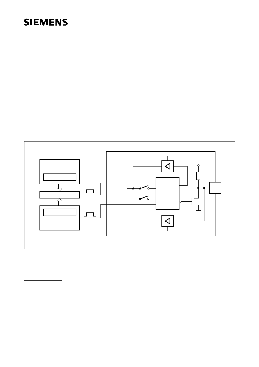
Compare Mode 0
In compare mode 0, upon matching the timer and compare register contents, the output signal
changes from low to high. It goes back to a low level on timer overflow. As long as compare mode
0 is enabled, the appropriate output pin is controlled by the timer circuit only and writing to the port
will have no effect. Figure 13 shows a functional diagram of a port circuit when used in compare
mode 0. The port latch is directly controlled by the timer overflow and compare match signals. The
input line from the internal bus and the write-to-latch line of the port latch are disconnected when
compare mode 0 is enabled.
Figure 13
Port Latch in Compare Mode 0
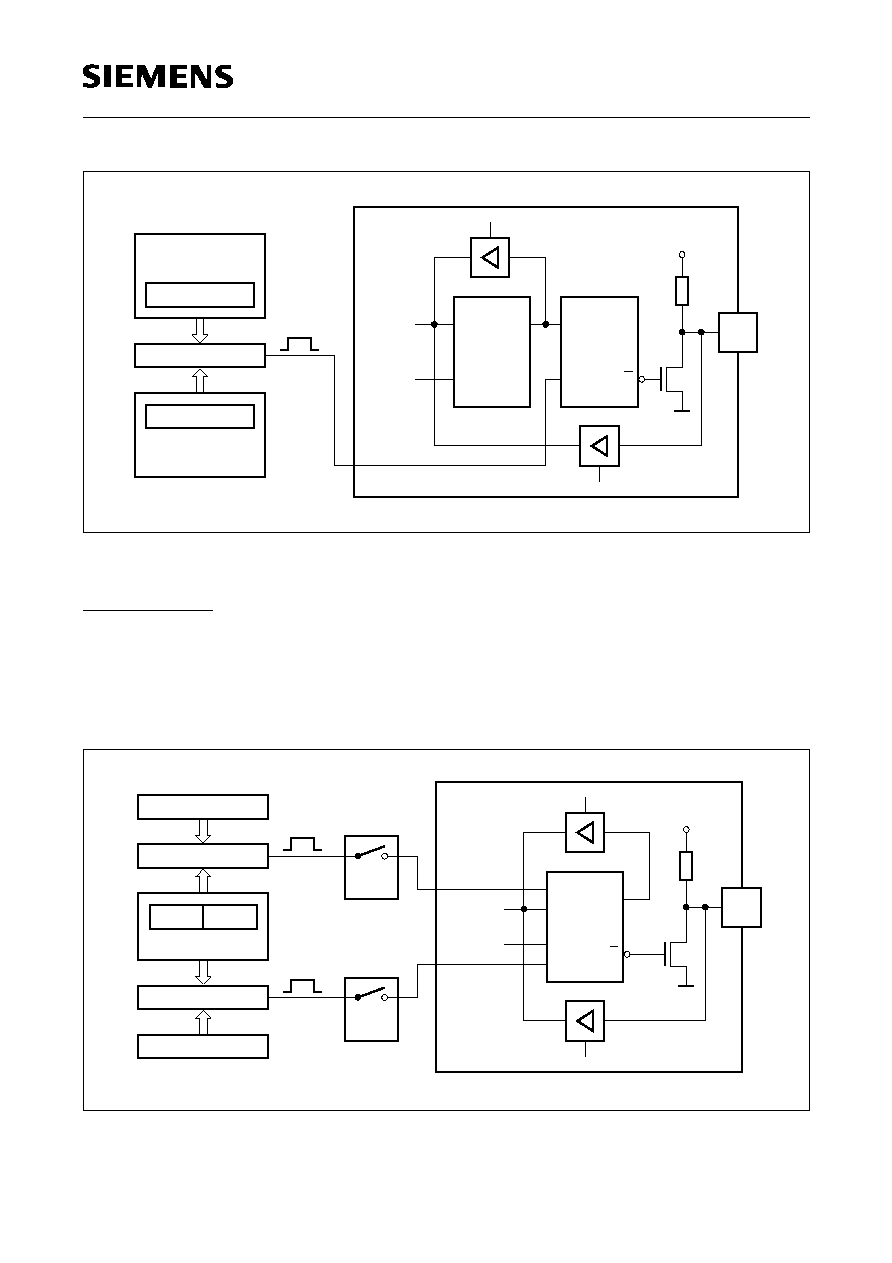
Compare Mode 1
If compare mode 1 is enabled and the software writes to the appropriate output latch at the port, the
new value will not appear at the output pin until the next compare match occurs. Thus, it can be
choosen whether the output signal has to make a new transition (1-to-0 or 0-to-1, depending on the
actual pin-level) or should keep its old value at the time when the timer value matches the stored
compare value.
In compare mode 1 (see figure 14) the port circuit consists of two separate latches. One latch
(which acts as a "shadow latch") can be written under software control, but its value will only be
transferred to the port latch (and thus to the port pin) when a compare match occurs.
MCS02661
Latch
Port
Q
Q
CLK
D
Port
Pin
Read Pin
CC
V
Read Latch
Port Circuit
Internal
Bus
Latch
Write to
Compare Reg.
Compare Register
Circuit
Comparator
Timer Register
Timer Circuit
Compare
Match
S
R
Overflow
Timer
16 Bit
Bit
16
C517A
Semiconductor Group
34
1997-10-01
Figure 14
Compare Function in Compare Mode 1
Compare Mode 2
In the compare mode 2 the port 5 pins are under control of compare/capture register CC4, but under
control of the compare registers COMSET and COMCLR. When a compare match occurs with
register COMSET, a high level appears at the pins of port 5 when the corresponding bits in the mask
register SETMSK are set. When a compare match occurs with register COMCLR, a low level
appears at the pins of port 5 when the corresponding bits in the mask register CLRMSK are set.
Figure 15
Compare Function of Compare Mode 2
MCS02662
Latch
Port
Q
Q
CLK
D
Read Pin
CC
V
D
CLK
Q
Shadow
Latch
Read Latch
Port Circuit
Internal
Bus
Latch
Write to
Compare Reg.
Compare Register
Circuit
Comparator
Timer Register
Timer Circuit
Compare
Match
Pin
Port
16 Bit
16 Bit
MCS02663
Latch
Port
Q
Q
CLK
D
Read Pin
CC
V
Read Latch
Port Circuit
Internal
Bus
Latch
Write to
Comparator
Compare
Signal
S
R
SETMSK
Bits
COMSET
TH2
Comparator
COMCLR
Timer 2
TL2
Bits
CLRMSK
Signal
Compare
Pin
Port
16 Bit
16 Bit
Bit
16
Bit
16
Semiconductor Group
35
1997-10-01
C517A
Multiplication / Division Unit (MDU)
This on-chip arithmetic unit of the C517A provides fast 32-bit division, 16-bit multiplication as well
as shift and normalize features. All operations are unsigned integer operations. Table 7 describes
the five general operations the MDU is able to perform.
1) 1
t
CY
= 12
t
CLCL
= 1 machine cycle = 500 ns at 24 MHz oscillator frequency
2) The maximal shift speed is 6 shifts per machine cycle
The MDU consists of seven special function registers (MD0-MD5, ARCON) which are used as
operand, result, and control registers. The three operation phases are shown in figure 16.
Figure 16
Operating Phases of the MDU
Table 7
MDU Operation Characteristics
Operation
Result
Remainder
Execution Time
32bit/16bit
16bit/16bit
16bit x 16bit
32-bit normalize
32-bit shift L/R
32bit
16bit
32bit
≠
≠
16bit
16bit
≠
≠
≠
6
t
CY
1)
4
t
CY
1)
4
t
CY
1)
6
t
CY
2)
6
t
CY
2)

C517A
Semiconductor Group
36
1997-10-01
For starting an operation, registers MD0 to MD5 and ARCON must be written to in a certain
sequence according table 8 and 9. The order the registers are accessed determines the type of the
operation. A shift operation is started by a final write operation to SFR ARCON.
Abbreviations:
D'end
: Dividend, 1st operand of division
D'or
: Divisor, 2nd operand of division
M'and
: Multiplicand, 1st operand of multiplication
M'or
: Multiplicator, 2nd operand of multiplication
Pr
: Product, result of multiplication
Rem
: Remainder
Quo
: Quotient, result of division
...L
: means, that this byte is the least significant of the 16-bit or 32-bit operand
...H
: means, that this byte is the most significant of the 16-bit or 32-bit operand
Table 8
Programming the MDU for Multiplication and Division
Operation
32Bit/16Bit
16Bit/16Bit
16Bit x 16Bit
First Write
Last Write
MD0
D'endL
MD1
D'end
MD2
D'end
MD3
D'endH
MD4
D'orL
MD5
D'orH
MD0
D'endL
MD1
D'endH
MD4
D'orL
MD5
D'orH
MD0
M'andL
MD4
M'orL
MD1
M'andH
MD5
M'orH
First Read
Last Read
MD0
QuoL
MD1
Quo
MD2
Quo
MD3
QuoH
MD4
RemL
MD5
RemH
MD0
QuoL
MD1
QuoH
MD4
RemL
MD5
RemH
MD0
PrL
MD1
MD2
MD3
PrH
Table 9
Programming of the MDU for a Shift or Normalize Operation
Operation
Normalize, Shift Left, Shift Right
First write
Last write
MD0
least significant byte
MD1
.
MD2
.
MD3
most significant byte
ARCON
start of conversion
First read
Last read
MD0
least significant byte
MD1
.
MD2
.
MD3
most significant byte
Semiconductor Group
37
1997-10-01
C517A
Serial Interfaces 0 and 1
The C517A has two serial interfaces which are functionally nearly identical concerning the
asynchronous modes of operation. The two channels are full-duplex, meaning they can transmit
and receive simultaneously. The serial channel 0 is completely compatible with the serial channel
of the C501 (one synchronous mode, three asynchronous modes). Serial channel 1 has the same
functionality in its asynchronous modes, but the synchronous mode and the fixed baud rate UART
mode is missing.
The operating modes of the serial interfaces is illustrated in table 10. The possible baudrates can
be calculated using the formulas given in table 11.
Table 10
Operating Modes of Serial Interface 0 and 1
Serial
Interface
Mode
S0CON
S1CON
Description
SM0
SM1
SM
0
0
0
0
≠
Shift register mode
Serial data enters and exits through R
◊
D0;
T
◊
D0 outputs the shift clock; 8-bit are
transmitted/received (LSB first); fixed baud rate
1
0
1
≠
8-bit UART, variable baud rate
10 bits are transmitted (through T
◊
D0) or
received (at R
◊
D0)
2
1
0
≠
9-bit UART, fixed baud rate
11 bits are transmitted (through T
◊
D0) or
received (at R
◊
D0)
3
1
1
≠
9-bit UART, variable baud rate
Like mode 2
1
A
≠
≠
0
9-bit UART; variable baud rate
11 bits are transmitted (through T
◊
D1) or
received (at R
◊
D1)
B
≠
≠
1
8-bit UART; variable baud rate
10 bits are transmitted (through T
◊
D1) or
received (at R
◊
D1)
C517A
Semiconductor Group
38
1997-10-01
For clarification some terms regarding the difference between "baud rate clock" and "baud rate"
should be mentioned. In the asynchronous modes the serial interfaces require a clock rate which is
16 times the baud rate for internal synchronization. Therefore, the baud rate generators/timers have
to provide a "baud rate clock" (output signal in figure 17 and figure 18) to the serial interface which -
there divided by 16 - results in the actual "baud rate". Further, the abbreviation f
OSC
refers to the
oscillator frequency (crystal or external clock operation).
The variable baud rates for modes 1 and 3 of the serial interface 0 can be derived from either timer 1
or a dedicated baud rate generator (see figure 17). The variable baud rates for modes A and B of
the serial interface 1 are derived from a dedicated baud rate generator as shown in figure 18.
Figure 17
Serial Interface 0 : Baud Rate Generation Configuration
Figure 18
Serial Interface 1 : Baud Rate Generator Configuration
The baud rate generator block in figure 17 has the same structure (10-bit auto-reload timer) as the
baud rate generator block which is shown in detail in figure 18.
MCS03329
f
OSC
(SM0/
SM1)
S0CON.7
S0CON.6
Only one mode
can be selected
ADCON0.7
(BD)
0
1
Timer 1 Overflow
Note : The switch configuration shows the reset state.
Mode 3
Mode 1
˜ 6
/2
Mode 2
Mode 0
Baud
Rate
Generator
(S0RELH
S0RELL)
˜ 2
(SMOD)
PCON.7
1
0
Rate
Baud
Clock
MCS03331
Baud Rate Generator
S1RELH
.1 .0
S1RELL
10-Bit Timer
Input Clock
Baud
Owerflow
f
/2
OSC
Rate
Clock
Semiconductor Group
39
1997-10-01
C517A
Table 11 below lists the values/formulas for the baud rate calculation of serial interface 0 and 1 with
its dependencies of the control bits BD and SMOD.
Table 11
Serial Interfaces - Baud Rate Dependencies
Serial Interface
Operating Modes
Active Control
Bits
Baud Rates
SMOD
BD
Mode 0 (Shift Register)
≠
≠
Fixed baud rate clock fosc/12
Mode 1 (8-bit UART)
Mode 3 (9-bit UART)
X
0
Timer 1 overflow is used for baud rate
generation; SMOD controls a divide-by-2 option.
Baud rate = 2
SMOD
x timer 1 overflow rate / 32
1
Baud rate generator is used for baud rate
generation; SMOD controls a divide-by-2 option
Baud rate = 2
SMOD
x oscillator frequency /
64 x (baud rate gen. overflow rate)
Mode 2 (9-bit UART)
X
≠
Fixed baud rate clock fosc/32 (SMOD=1) or fosc/
64 (SMOD=0)
Mode A (9-bit UART)
Mode B (8-bit UART)
≠
≠
Baud rate generator is used for baud rate
generation; SMOD controls a divide-by-2 option
Baud rate = oscillator frequency /
32 x (baud rate gen. overflow rate)

C517A
Semiconductor Group
40
1997-10-01
10-Bit A/D Converter
The C517A provides an A/D converter with the following features:
≠ 12 multiplexed input channels (port 7, 8), which can also be used as digital inputs
≠ 10-bit resolution
≠ Single or continuous conversion mode
≠ Internal or external start-of-conversion trigger capability
≠ Interrupt request generation after each conversion
≠ Using successive approximation conversion technique via a capacitor array
≠ Built-in hidden calibration of offset and linearity errors
The A/D converter operates with a successive approximation technique and uses self calibration
mechanisms for reduction and compensation of offset and linearity errors. The externally applied
reference voltage range has to be held on a fixed value within the specifications. The main
functional blocks of the A/D converter are shown in figure 19.
Semiconductor Group
41
1997-10-01
C517A
Figure 19
A/D Converter Block Diagram
A/D
Converter
ADDATH ADDATL
ADCON0 (D8 )
internal
MUX
Port 7
S&H
f
ADC
OSC
f
V
AREF
V
AGND
P6.0/ADST
Shaded bit locations are not used in ADC-functions
MCB03332
Single/
Continuous Mode
)
(D9
(DA )
H
Clock
Prescaler
˜8, ˜4
P7.7
P7.6
P7.5
P7.4
P7.3
P7.2
P7.1
P7.0
ADCON1 (DC )
H
P7 (DB )
H
P8 (DD )
H
IRCON0 (C0 )
H
IEN1 (B8 )
H
Port 8
Bus
/2
Write to ADDATL
Conversion
Clock
Input
Clock
IN
f
Start of
Conversion
internal
Bus
IEX5
BSY
EX5
CLK
ADCL
BD
ADEX
_
_
TF2
_
EXF2
_
_
IEX6
SWDT
EXEN2
EX6
MX3
ADM
_
MX2
MX1
MX2
MX1
IEX3
P8.3
_
IEX4
P8.2
P8.1
IEX2
MX0
MX0
P8.0
IADC
EADC
EX4
EX3
EX2
.8
MSB
.6
.7
.4
.5
.2
.3
.1
LSB
_
_
_
_
_
_
H
H

C517A
Semiconductor Group
42
1997-10-01
Interrupt System
The C517A provides 17 interrupt sources with four priority levels. Ten interrupts can be generated
by the on-chip peripherals (timer 0, timer 1, timer 2, compare timer, compare match/set/clear, A/D
converter, and serial interface 0 and 1) and seven interrupts may be triggered externally (P3.2/INT0,
P3.3/INT1, P1.4/INT2, P1.0/INT3, P1.1/INT4, P1.2/INT5, P1.3/INT6).
This chapter shows the interrupt structure, the interrupt vectors and the interrupt related special
function registers. Figure 20 to 22 give a general overview of the interrupt sources and illustrate the
request and the control flags which are described in the next sections.

Semiconductor Group
43
1997-10-01
C517A
Figure 20
Interrupt Structure, Overview (Part 1)
MCS03333
Bit addressable
Request Flag is
cleared by hardware
IP1.0
H
0003
TCON.1
IEN0.0
IE0
EX0
P3.2/
IT0
TCON.0
IP0.0
Highest
Priority Level
ES1
RI1
IEN2.0
S1CON.0
0083 H
UART 1
Timer 0
H
000B
TCON.5
IEN0.1
TF0
ET0
Overflow
INT0
INT2/
T2CON.5
I2FR
P1.4/
EX2
IEX2
IEN1.1
IRCON0.1
Lowest
Priority Level
EAL
IEN0.7
Polling Sequence
004B H
IP0.1
IP1.1
1
_
<
TI1
S1CON.1
CC4
A/D Converter
0043
IRCON0.0
IEN1.0
EADC
IADC
H
C517A
Semiconductor Group
44
1997-10-01
Figure 21
Interrupt Structure, Overview (Part 2)
MCS03334
Bit addressable
Request Flag is
cleared by hardware
IP1.2
H
0013
TCON.3
IEN0.2
IE1
EX1
P3.3/
IT1
TCON.2
IP0.2
Highest
Priority Level
ECMP
IEN2.2
0093 H
Match in CM0-CM7
Timer 1
H
001B
TCON.7
IEN0.3
TF1
ET1
Overflow
INT1
ECT
CTF
IEN2.3
CTCON.3
Lowest
Priority Level
EAL
IEN0.7
Polling Sequence
009B H
IP0.3
IP1.3
0053 H
IRCON1.0-7
ICMP0-7
I3FR
T2CON.5
CC0
P1.0/
INT3/
IRCON0.2
IEN1.2
IEX3
EX3
Overflow
Compare Timer
IRCON0.3
IEX4
005B
IEN1.3
EX4
H
CC1
INT4/
P1.1/
Semiconductor Group
45
1997-10-01
C517A
Figure 22
Interrupt Structure, Overview (Part 3)
MCS03335
Bit addressable
Request Flag is
cleared by hardware
IP1.4
H
0023
IP0.4
Highest
Priority Level
ES0
RI0
IEN0.4
S0CON.0
00A3 H
USART 0
Timer 2
H
002B
IEN0.5
ET2
Overflow
INT6/
P1.3/
EX6
IEX6
IEN1.5
IRCON0.5
Lowest
Priority Level
EAL
IEN0.7
Polling Sequence
006B H
IP0.5
IP1.5
1
_
<
TI0
S0CON.1
CC3
0063
IRCON0.4
IEN1.4
EX5
IEX5
H
CTCON.4
ECS
IEN2.4
ICS
TF2
IRCON0.6
_
< 1
00AB
CTCON.5
IEN2.5
ICR
ECR
H
IRCON0.7
EXF2
IEN1.7
EXEN2
P1.2/
INT5/
CC2
P1.5/
T2EX
Match in COMSET
Match in COMCLR
C517A
Semiconductor Group
46
1997-10-01
Table 12
Interrupt Source and Vectors
Interrupt Source
Interrupt Vector Address
Interrupt Request Flags
External Interrupt 0
0003H
IE0
Timer 0 Overflow
000BH
TF0
External Interrupt 1
0013H
IE1
Timer 1 Overflow
001BH
TF1
Serial Channel 0
0023H
RI0 / TI0
Timer 2 Overflow / Ext. Reload
002BH
TF2 / EXF2
A/D Converter
0043H
IADC
External Interrupt 2
004BH
IEX2
External Interrupt 3
0053H
IEX3
External Interrupt 4
005BH
IEX4
External Interrupt 5
0063H
IEX5
External Interrupt 6
006BH
IEX6
Serial Channel 1
0083H
RI1 / TI1
Compare Match Interrupt of
Compare Registers CM0-CM7
assigned to Timer 2
0093H
ICMP0 - ICMP7
Compare Timer Overflow
009BH
CTF
Compare Match Interrupt of
Compare Register COMSET
00A3H
ICS
Compare Match Interrupt of
Compare Register COMCLR
00ABH
ICR

Semiconductor Group
47
1997-10-01
C517A
Fail Save Mechanisms
The C517A offers enhanced fail safe mechanisms, which allow an automatic recovery from
software upset or hardware failure:
≠ a programmable watchdog timer (WDT), with variable time-out period from 512
µ
s up to
approx. 1.1 s at 12 MHz. (256
µ
s up to approx. 0.65 s at 24 MHz)
≠ an oscillator watchdog (OWD) which monitors the on-chip oscillator and forces the
microcontroller into reset state in case the on-chip oscillator fails; it also provides the clock for
a fast internal reset after power-on.
The watchdog timer in the C517A is a 15-bit timer, which is incremented by a count rate of
f
OSC
/24
up to
f
OSC
/384. The system clock of the C517A is divided by two prescalers, a divide-by-two and a
divide-by-16 prescaler. For programming of the watchdog timer overflow rate, the upper 7 bit of the
watchdog timer can be written. Figure 23 shows the block diagram of the watchdog timer unit.
Figure 23
Block Diagram of the Watchdog Timer
The watchdog timer can be started by software (bit SWDT) or by hardware through pin PE/SWD,
but it cannot be stopped during active mode of the C517A. If the software fails to refresh the running
watchdog timer an internal reset will be initiated on watchdog timer overflow. For refreshing of the
watchdog timer the content of the SFR WDTREL is transferred to the upper 7-bit of the watchdog
timer. The refresh sequence consists of two consecutive instructions which set the bits WDT and
SWDT each. The reset cause (external reset or reset caused by the watchdog) can be examined
by software (flag WDTS). It must be noted, however, that the watchdog timer is halted during the
idle mode and power down mode of the processor.
MCB03250
IP0 (A9 )
H
OSC
f
WDTS
-
-
-
-
-
-
-
2
16
14
0
7
8
WDTL
WDTH
/12
External HW Reset
External HW Power-Down
PE/SWD
Control Logic
IEN0 (A8 )H
IEN1 (B8 )H
6
7
0
WDT Reset-Request
WDTPSEL
WDTREL (86 )
H
-
WDT
-
-
-
-
-
-
-
SWDT
-
-
-
-
-
-
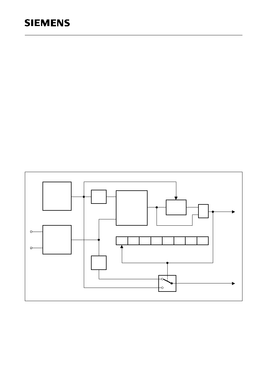
C517A
Semiconductor Group
48
1997-10-01
Oscillator Watchdog
The oscillator watchdog unit serves for four functions:
≠ Monitoring of the on-chip oscillator's function
The watchdog supervises the on-chip oscillator's frequency; if it is lower than the frequency
of the auxiliary RC oscillator in the watchdog unit, the internal clock is supplied by the RC
oscillator and the device is brought into reset; if the failure condition disappears (i.e. the on-
chip oscillator has a higher frequency than the RC oscillator), the part executes a final reset
phase of typ. 1 ms in order to allow the oscillator to stabilize; then the oscillator watchdog reset
is released and the part starts program execution again.
≠ Fast internal reset after power-on
The oscillator watchdog unit provides a clock supply for the reset before the on-chip oscillator
has started. The oscillator watchdog unit also works identically to the monitoring function.
≠ Restart from the hardware power down mode.
If the hardware power down mode is terminated the oscillator watchdog has to control the
correct start-up of the on-chip oscillator and to restart the program. The oscillator watchdog
function is only part of the complete hardware power down sequence; however, the watchdog
works identically to the monitoring function.
Figure 24
Block Diagram of the Oscillator Watchdog
OWDS
1
IP0 (A9 )
Frequency
Comparator
Delay
f
2
<
1
f
f
1
2
f
Internal Clock
On-Chip
Oscillator
Oscillator
RC
XTAL1
XTAL2
RC
f
3MHz
MCB03337
H
˜ 5
˜ 2
_
<
Internal Reset

Semiconductor Group
49
1997-10-01
C517A
Power Saving Modes
The C517A provides two basic power saving modes, the idle mode and the power down mode.
Additionally, a slow down mode is available. This power saving mode reduces the internal clock rate
in normal operating mode and it can be also used for further power reduction in idle mode.
≠ Idle mode
The CPU is gated off from the oscillator. All peripherals are still provided with the clock and
are able to work. Idle mode is entered by software and can be left by an interrupt or reset.
≠ Slow down mode
The controller keeps up the full operating functionality, but its normal clock frequency is
internally divided by 8. This slows down all parts of the controller, the CPU and all peripherals,
to 1/8th of their normal operating frequency and also reduces power consumption.
≠ Software power down mode
The operation of the C517A is completely stopped and the oscillator is turned off. This mode
is used to save the contents of the internal RAM with a very low standby current. This power
down mode is entered by software and can be left by reset or by a short low pulse at pin P3.2/
INT0.
≠ Hardware Power down mode
If pin HWPD gets active (low level) the part enters the hardware power down mode and starts
a complete internal reset sequence. Thereafter, both oscillators of the chip are stopped and
the port pins and several control lines enter a floating state.
In the power down mode of operation,
V
CC
can be reduced to minimize power consumption. It must
be ensured, however, that
V
CC
is not reduced before the power down mode is invoked, and that
V
CC
is restored to its normal operating level, before the power down mode is terminated. Table 13 gives
a general overview of the entry and exit procedures of the power saving modes.
C517A
Semiconductor Group
50
1997-10-01
Table 13
Power Saving Modes Overview
Mode
Entering
2-Instruction
Example
Leaving by
Remarks
Idle mode
ORL PCON, #01H
ORL PCON, #20H
Occurrence of an
interrupt from a
peripheral unit
CPU clock is stopped;
CPU maintains their data;
peripheral units are active (if
enabled) and provided with
clock
Hardware Reset
Slow Down Mode
In normal mode:
ORL PCON,#10H
ANL PCON,#0EFH
or
Hardware Reset
Internal clock rate is reduced
to 1/8 of its nominal frequency
With idle mode:
ORL PCON,#01H
ORL PCON, #30H
Occurrence of an
interrupt from a
peripheral unit
CPU clock is stopped;
CPU maintains their data;
peripheral units are active (if
enabled) and provided with 1/8
of its nominal frequency
Hardware reset
Software
Power Down Mode
ORL PCON, #02H
ORL PCON, #40H
Hardware Reset
Oscillator is stopped;
contents of on-chip RAM and
SFR's are maintained;
Short low pulse at
pin P3.2/INT0
Hardware
Power Down Mode
HWPD = 0
HWPD = 1
Oscillator is stopped; internal
reset is executed;

Semiconductor Group
51
1997-10-01
C517A
Absolute Maximum Ratings
Ambient temperature under bias (
T
A
) ......................................................... ≠ 40 to 125
∞
C
Storage temperature (
T
stg
) .......................................................................... ≠ 65
∞
C to 150
∞
C
Voltage on
V
CC
pins with respect to ground (
V
SS
) ....................................... ≠ 0.5 V to 6.5 V
Voltage on any pin with respect to ground (
V
SS
) ......................................... ≠ 0.5 V to
V
CC
+0.5 V
Input current on any pin during overload condition ..................................... ≠ 10 mA to 10 mA
Absolute sum of all input currents during overload condition ..................... I 100 mA I
Power dissipation........................................................................................ TBD
Note: Stresses above those listed under "Absolute Maximum Ratings" may cause permanent
damage of the device. This is a stress rating only and functional operation of the device at
these or any other conditions above those indicated in the operational sections of this
specification is not implied. Exposure to absolute maximum rating conditions for longer
periods may affect device reliability. During overload conditions (
V
IN
>
V
CC
or
V
IN
<
V
SS
) the
Voltage on
V
CC
pins with respect to ground (
V
SS
) must not exceed the values defined by the
absolute maximum ratings.
C517A
Semiconductor Group
52
1997-10-01
DC Characteristics
V
CC
= 5 V + 10%, ≠ 15%;
V
SS
= 0 V
T
A
= 0 to 70
∞
C
for the SAB-C517A
T
A
= ≠ 40 to 85
∞
C
for the SAF-C517A
T
A
= ≠ 40 to 110
∞
C
for the SAH-C517A
Notes see next page
Parameter
Symbol
Limit Values
Unit
Test Condition
min.
max.
Input low voltage
Pins except EA,RESET,HWPD
EA pin
HWPD and RESET pins
V
IL
V
IL1
V
IL2
≠ 0.5
≠ 0.5
≠ 0.5
0.2
V
CC
≠ 0.1
0.2
V
CC
≠ 0.3
0.2
V
CC
+ 0.1
V
V
V
≠
≠
≠
Input high voltage
pins except RESET, XTAL2 and
HWPD
XTAL2 pin
RESET and HWPD pin
V
IH
V
IH1
V
IH2
0.2
V
CC
+ 0.9
0.7
V
CC
0.6
V
CC
V
CC
+ 0.5
V
CC
+ 0.5
V
CC
+ 0.5
V
V
V
≠
≠
≠
Output low voltage
Ports 1, 2, 3, 4, 5, 6
Port 0, ALE, PSEN, RO
V
OL
V
OL1
≠
≠
0.45
0.45
V
V
I
OL
= 1.6 mA
1)
I
OL
= 3.2 mA
1)
Output high voltage
Ports 1, 2, 3, 4, 5, 6
Port 0 in external bus mode,
ALE, PSEN, RO
V
OH
V
OH1
2.4
0.9
V
CC
2.4
0.9
V
CC
≠
≠
≠
≠
V
V
V
V
I
OH
= ≠ 80
µ
A
I
OH
= ≠ 10
µ
A
I
OH
= ≠ 800
µ
A
I
OH
= ≠ 80
µ
A
2)
Logic 0 input current
Ports 1, 2, 3, 4, 5, 6
I
LI
≠ 10
≠ 70
µ
A
V
I N
= 0.45 V
Logical 0-to-1 transition current,
Ports 1, 2, 3, 4, 5, 6
I
TL
≠ 65
≠ 650
µ
A
V
I N
= 2 V
Input leakage current
Port 0, 7 and 8, EA, HWPD
I
LI
≠
±
1
µ
A
0.45 <
V
I N
<
V
CC
Input low current
to RESET for reset
XTAL2
PE/SWD, OWE
I
IL2
I
IL3
I
IL4
≠ 10
≠
≠
≠ 100
≠ 15
≠ 20
µ
A
µ
A
µ
A
V
I N
= 0.45 V
V
I N
= 0.45 V
V
I N
= 0.45 V
Pin capacitance
C
IO
≠
10
pF
f
C
= 1 MHz,
T
A
= 25
∞
C
Overload current
I
OV
≠
±
5
mA
7) 8)
Semiconductor Group
53
1997-10-01
C517A
Power Supply Current
Notes:
1) Capacitive loading on ports 0 and 2 may cause spurious noise pulses to be superimposed on the
V
OL
of ALE
and port 3. The noise is due to external bus capacitance discharging into the port 0 and port 2 pins when these
pins make 1-to-0 transitions during bus operation. In the worst case (capacitive loading > 100 pF), the noise
pulse on ALE line may exceed 0.8 V. In such cases it may be desirable to qualify ALE with a schmitt-trigger,
or use an address latch with a schmitt-trigger strobe input.
2) Capacitive loading on ports 0 and 2 may cause the
V
OH
on ALE and PSEN to momentarily fall below the
0.9
V
CC
specification when the address lines are stabilizing.
3)
I
PD
(power-down mode) is measured under following conditions:
EA = RESET = Port 0 = Port 7 = Port 8 =
V
CC
; XTAL1 = N.C.; XTAL2 =
V
SS
; PE/SWD = OWE =
V
SS
;
HWPD =
V
CC
for software power-down mode;
V
AGND
=
V
SS
;
V
AREF
=
V
CC
; all other pins are disconnected.
I
PD
(hardware power-down mode) is independent of any particular pin connection.
4)
I
CC
(active mode) is measured with:
XTAL2 driven with
t
CLCH
,
t
CHCL
= 5 ns ,
V
IL
=
V
SS
+ 0.5 V,
V
IH
=
V
CC
≠ 0.5 V; XTAL1 = N.C.;
EA = PE/SWD ==
V
SS
; Port 0 = Port 7 = Port 8 =
V
CC
; HWPD =
V
CC
; RESET =
V
CC
; all other pins are
disconnected.
5)
I
CC
(idle mode) is measured with all output pins disconnected and with all peripherals disabled;
XTAL2 driven with
t
CLCH
,
t
CHCL
= 5 ns,
V
IL
=
V
SS
+ 0.5 V,
V
IH
=
V
CC
≠ 0.5 V; XTAL1 = N.C.;
RESET =
V
CC
; HWPD = Port 0 = Port 7 = Port 8 =
V
CC
; EA = PE/SWD =
V
SS
;
all other pins are disconnected;
6)
I
CC
(active mode with slow-down mode) is measured with all output pins disconnected and with all peripherals
disabled; XTAL2 driven with
t
CLCH
,
t
CHCL
= 5 ns ,
V
IL
=
V
SS
+ 0.5 V,
V
IH
=
V
CC
≠ 0.5 V; XTAL1 = N.C.;
HWPD =
V
CC
; RESET =
V
CC
; Port 7 = Port 8 =
V
CC
;; EA = PE/SWD ==
V
SS
; all other pins are disconnected.
7) Overload conditions occur if the standard operating conditions are exceeded, i.e. the voltage on any pin
exceeds the specified range (i.e.
V
OV
>
V
CC
+ 0.5 V or
V
OV
<
V
SS
- 0.5 V). The supply voltage
V
CC
and
V
SS
must
remain within the specified limits. The absolute sum of input currents on all port pins may not exceed 50 mA.
8) Not 100% tested, guaranteed by design characterization
9) The typical
I
CC
values are periodically measured at
T
A
= +25
∞
C and
V
CC
= 5 V but not 100% tested.
10)The maximum
I
CC
values are measured under worst case conditions (
T
A
= 0
∞
C or -40
∞
C and
V
CC
= 5.5 V)
Parameter
Symbol
Limit Values
Unit Test Condition
typ.
9)
max.
10)
Active mode
18 MHz
24 MHz
I
CC
I
CC
21.3
27.3
29.2
37.6
mA
mA
4)
Idle mode
18 MHz
24 MHz
I
CC
I
CC
11.6
14.6
16.2
20.4
mA
mA
5)
Active mode with
slow-down enabled
18 MHz
24 MHz
I
CC
I
CC
9.5
10.7
13.1
14.9
mA
mA
6)
Power-down mode
I
PD
15
50
µ
A
V
CC
= 2
...
5.5 V
3)
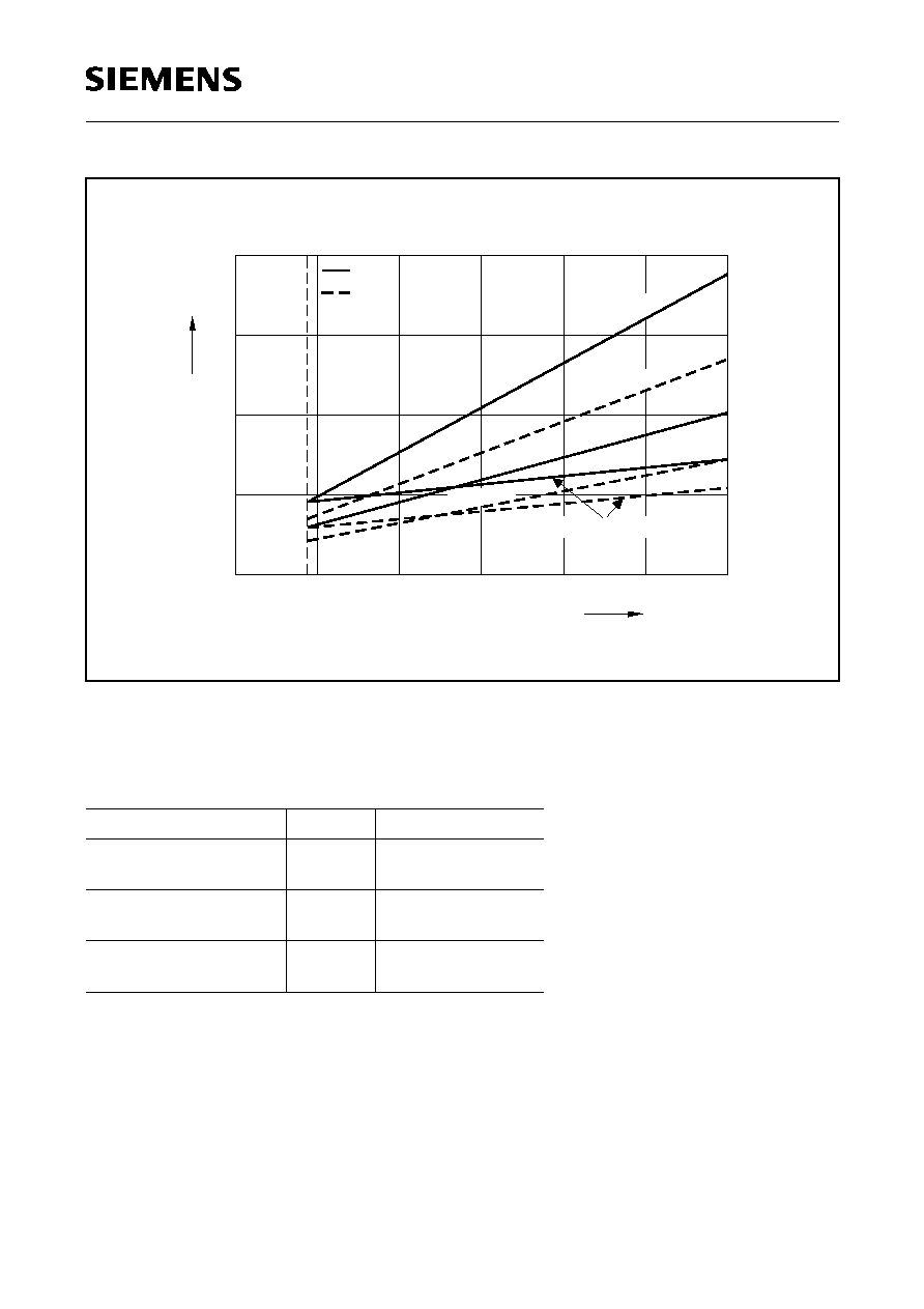
C517A
Semiconductor Group
54
1997-10-01
Figure 25
ICC Diagram
Note:
f
osc
is the oscillator frequency in MHz.
I
CC
values are given in mA.
Table 14
Power Supply Current Calculation Formulas
Parameter
Symbol
Formula
Active mode
I
CC typ
I
CC max
1
*
f
OSC
+ 3.3
1.4
*
f
OSC
+ 4.0
Idle mode
I
CC typ
I
CC max
0.5
*
f
OSC
+ 2.6
0.7
*
f
OSC
+ 3.6
Active mode with
slow-down enabled
I
CC typ
I
CC max
0.25
*
f
OSC
+ 4.95
0.3
*
f
OSC
+ 7.7
MCD03338
0
0
f
OSC
CC
3.5
8
12
16
20
24
MHz
mA
CC typ
CC max
10
20
30
40
Active Mode
Idle Mode
Idle Mode
Active Mode
Active + Slow Down Mode
Semiconductor Group
55
1997-10-01
C517A
A/D Converter Characteristics
V
CC
= 5 V + 10%, ≠ 15%;
V
SS
= 0 V
T
A
= 0 to 70
∞
C
for the SAB-C517A
T
A
= ≠ 40 to 85
∞
C
for the SAF-C517A
T
A
= ≠ 40 to 110
∞
C
for the SAH-C517A
4 V
V
AREF
V
CC
+0.1 V;
V
SS
-0.1 V
V
AGND
V
SS
+0.2 V
Notes see next page.
Clock calculation table:
Further timing conditions:
t
ADC
min = 500 ns
t
IN
= 2 / f
OSC
= 2 t
CLCL
Parameter
Symbol
Limit Values
Unit
Test Condition
min.
max.
Analog input voltage
V
AIN
V
AGND
V
AREF
V
1)
Sample time
t
S
≠
16 x
t
IN
8 x
t
IN
ns
Prescaler
˜
8
Prescaler
˜
4
2)
Conversion cycle time
t
ADCC
≠
96 x
t
IN
48 x
t
IN
ns
Prescaler
˜
8
Prescaler
˜
4
3)
Total unadjusted error
T
UE
≠
±
2
LSB
V
SS
+0.5V
V
IN
V
CC
-0.5V
4)
Internal resistance of
reference voltage source
R
AREF
≠
t
ADC
/ 250
- 0.25
k
t
ADC
in [ns]
5) 6)
Internal resistance of
analog source
R
ASRC
≠
t
S
/ 500
- 0.25
k
t
S
in [ns]
2) 6)
ADC input capacitance
C
AIN
≠
50
pF
6)
Clock Prescaler
Ratio
ADCL
t
ADC
t
S
t
ADCC
˜
8
1
8 x t
IN
16 x t
IN
96 x t
IN
˜
4
0
4 x t
IN
8 x t
IN
48 x t
IN

C517A
Semiconductor Group
56
1997-10-01
Notes:
1) V
AIN
may exceed V
AGND
or V
AREF
up to the absolute maximum ratings. However, the conversion result in
these cases will be X000
H
or X3FF
H
, respectively.
2) During the sample time the input capacitance
C
AIN
can be charged/discharged by the external source. The
internal resistance of the analog source must allow the capacitance to reach their final voltage level within t
S
.
After the end of the sample time t
S
, changes of the analog input voltage have no effect on the conversion
result.
3) This parameter includes the sample time t
S
, the time for determining the digital result and the time for the
calibration. Values for the conversion clock t
ADC
depend on programming and can be taken from the table on
the previous page.
4) T
UE
is tested at V
AREF
= 5.0 V, V
AGND
= 0 V, V
CC
= 4.9 V. It is guaranteed by design characterization for all
other voltages within the defined voltage range.
If an overload condition occurs on maximum 2 not selected analog input pins and the absolute sum of input
overload currents on all analog input pins does not exceed 10 mA, an additional conversion error of 1/2 LSB
is permissible.
5) During the conversion the ADC's capacitance must be repeatedly charged or discharged. The internal
resistance of the reference source must allow the capacitance to reach their final voltage level within the
indicated time. The maximum internal resistance results from the programmed conversion timing.
6) Not 100% tested, but guaranteed by design characterization.

Semiconductor Group
57
1997-10-01
C517A
AC Characteristics (18 MHz)
V
CC
= 5 V + 10%, ≠ 15%;
V
SS
= 0 V
T
A
= 0 to 70
∞
C
for the SAB-C517A
T
A
= ≠ 40 to 85
∞
C
for the SAF-C517A
T
A
= ≠ 40 to 110
∞
C
for the SAH-C517A
(
C
L
for port 0, ALE and PSEN outputs = 100 pF;
C
L
for all other outputs = 80 pF)
Program Memory Characteristics
*)
Interfacing the C517A to devices with float times up to 45 ns is permissible. This limited bus contention will not
cause any damage to port 0 drivers.
Parameter
Symbol
Limit Values
Unit
18 MHz
Clock
Variable Clock
1/
t
CLCL
= 3.5 MHz to 18 MHz
min.
max.
min.
max.
ALE pulse width
t
LHLL
71
≠
2
t
CLCL
≠ 40
≠
ns
Address setup to ALE
t
AVLL
26
≠
t
CLCL
≠ 30
≠
ns
Address hold after ALE
t
LLAX
26
≠
t
CLCL
≠ 30
≠
ns
ALE low to valid instruction in
t
LLIV
≠
122
≠
4
t
CLCL
≠ 100
ns
ALE to PSEN
t
LLPL
31
≠
t
CLCL
≠ 25
≠
ns
PSEN pulse width
t
PLPH
132
≠
3
t
CLCL
≠ 35
≠
ns
PSEN to valid instruction in
t
PLIV
≠
92
≠
3
t
CLCL
≠ 75
ns
Input instruction hold after PSEN
t
PXIX
0
≠
0
≠
ns
Input instruction float after PSEN
t
PXIZ
*)
≠
46
≠
t
CLCL
≠ 10
ns
Address valid after PSEN
t
PXAV
*)
48
≠
t
CLCL
≠ 8
≠
ns
Address to valid instr in
t
AVIV
≠
180
≠
5
t
CLCL
≠ 98
ns
Address float to PSEN
t
AZPL
0
≠
0
≠
ns

C517A
Semiconductor Group
58
1997-10-01
AC Characteristics (18 MHz, cont'd)
External Data Memory Characteristics
External Clock Drive Characteristics
Parameter
Symbol
Limit Values
Unit
18 MHz
Clock
Variable Clock
1/
t
CLCL
= 3.5 MHz to 18 MHz
min.
max.
min.
max.
RD pulse width
t
RLRH
233
≠
6
t
CLCL
≠ 100
≠
ns
WR pulse width
t
WLWH
233
≠
6
t
CLCL
≠ 100
≠
ns
Address hold after ALE
t
LLAX2
81
≠
2
t
CLCL
≠ 30
≠
ns
RD to valid data in
t
RLDV
≠
128
≠
5
t
CLCL
≠ 150
ns
Data hold after RD
t
RHDX
0
≠
0
≠
ns
Data float after RD
t
RHDZ
≠
51
≠
2
t
CLCL
≠ 60
ns
ALE to valid data in
t
LLDV
≠
294
≠
8
t
CLCL
≠ 150
ns
Address to valid data in
t
AVDV
≠
335
≠
9
t
CLCL
≠ 165
ns
ALE to WR or RD
t
LLWL
117
217
3
t
CLCL
≠ 50
3
t
CLCL
+ 50
ns
Address valid to WR or RD
t
AVWL
92
≠
4
t
CLCL
≠ 130
≠
ns
WR or RD high to ALE high
t
WHLH
16
96
t
CLCL
≠ 40
t
CLCL
+ 40
ns
Data valid to WR transition
t
QVWX
11
≠
t
CLCL
≠ 45
≠
ns
Data setup before WR
t
QVWH
239
≠
7
t
CLCL
≠ 150
≠
ns
Data hold after WR
t
WHQX
16
≠
t
CLCL
≠ 40
≠
ns
Address float after RD
t
RLAZ
≠
0
≠
0
ns
Parameter
Symbol
Limit Values
Unit
Variable Clock
Freq. = 3.5 MHz to 18 MHz
min.
max.
Oscillator period
t
CLCL
55.6
285.7
ns
High time
t
CHCX
15
t
CLCL
≠
t
CLCX
ns
Low time
t
CLCX
15
t
CLCL
≠
t
CHCX
ns
Rise time
t
CLCH
≠
15
ns
Fall time
t
CHCL
≠
15
ns
Semiconductor Group
59
1997-10-01
C517A
AC Characteristics (24 MHz)
V
CC
= 5 V + 10%, ≠ 15%;
V
SS
= 0 V
T
A
= 0 to 70
∞
C
for the SAB-C517A
T
A
= ≠ 40 to 85
∞
C
for the SAF-C517A
T
A
= ≠ 40 to 110
∞
C
for the SAH-C517A
(
C
L
for port 0, ALE and PSEN outputs = 100 pF;
C
L
for all other outputs = 80 pF)
Program Memory Characteristics
*)
Interfacing the C517A to devices with float times up to 37 ns is permissible. This limited bus contention will not
cause any damage to port 0 drivers.
Parameter
Symbol
Limit Values
Unit
24 MHz
Clock
Variable Clock
1/
t
CLCL
= 3.5 MHz to 24 MHz
min.
max.
min.
max.
ALE pulse width
t
LHLL
43
≠
2
t
CLCL
≠ 40
≠
ns
Address setup to ALE
t
AVLL
17
≠
t
CLCL
≠ 25
≠
ns
Address hold after ALE
t
LLAX
17
≠
t
CLCL
≠ 25
≠
ns
ALE low to valid instruction in
t
LLIV
≠
80
≠
4
t
CLCL
≠ 87
ns
ALE to PSEN
t
LLPL
22
≠
t
CLCL
≠ 20
≠
ns
PSEN pulse width
t
PLPH
95
≠
3
t
CLCL
≠ 30
≠
ns
PSEN to valid instruction in
t
PLIV
≠
60
≠
3
t
CLCL
≠ 65
ns
Input instruction hold after PSEN
t
PXIX
0
≠
0
≠
ns
Input instruction float after PSEN
t
PXIZ
*)
≠
32
≠
t
CLCL
≠ 10
ns
Address valid after PSEN
t
PXAV
*)
37
≠
t
CLCL
≠ 5
≠
ns
Address to valid instr in
t
AVIV
≠
148
≠
5
t
CLCL
≠ 60
ns
Address float to PSEN
t
AZPL
0
≠
0
≠
ns

C517A
Semiconductor Group
60
1997-10-01
AC Characteristics (24 MHz, cont'd)
External Data Memory Characteristics
External Clock Drive Characteristics
Parameter
Symbol
Limit Values
Unit
24 MHz
Clock
Variable Clock
1/
t
CLCL
= 3.5 MHz to 24 MHz
min.
max.
min.
max.
RD pulse width
t
RLRH
180
≠
6
t
CLCL
≠ 70
≠
ns
WR pulse width
t
WLWH
180
≠
6
t
CLCL
≠ 70
≠
ns
Address hold after ALE
t
LLAX2
53
≠
2
t
CLCL
≠ 30
≠
ns
RD to valid data in
t
RLDV
≠
118
≠
5
t
CLCL
≠ 90
ns
Data hold after RD
t
RHDX
0
≠
0
≠
ns
Data float after RD
t
RHDZ
≠
63
≠
2
t
CLCL
≠ 20
ns
ALE to valid data in
t
LLDV
≠
200
≠
8
t
CLCL
≠ 133
ns
Address to valid data in
t
AVDV
≠
220
≠
9
t
CLCL
≠ 155
ns
ALE to WR or RD
t
LLWL
75
175
3
t
CLCL
≠ 50
3
t
CLCL
+ 50
ns
Address valid to WR or RD
t
AVWL
67
≠
4
t
CLCL
≠ 97
≠
ns
WR or RD high to ALE high
t
WHLH
17
67
t
CLCL
≠ 25
t
CLCL
+ 25
ns
Data valid to WR transition
t
QVWX
5
≠
t
CLCL
≠ 37
≠
ns
Data setup before WR
t
QVWH
170
≠
7
t
CLCL
≠ 122
≠
ns
Data hold after WR
t
WHQX
15
≠
t
CLCL
≠ 27
≠
ns
Address float after RD
t
RLAZ
≠
0
≠
0
ns
Parameter
Symbol
Limit Values
Unit
Variable Clock
Freq. = 3.5 MHz to 24 MHz
min.
max.
Oscillator period
t
CLCL
41.7
285.7
ns
High time
t
CHCX
12
t
CLCL
≠
t
CLCX
ns
Low time
t
CLCX
12
t
CLCL
≠
t
CHCX
ns
Rise time
t
CLCH
≠
12
ns
Fall time
t
CHCL
≠
12
ns
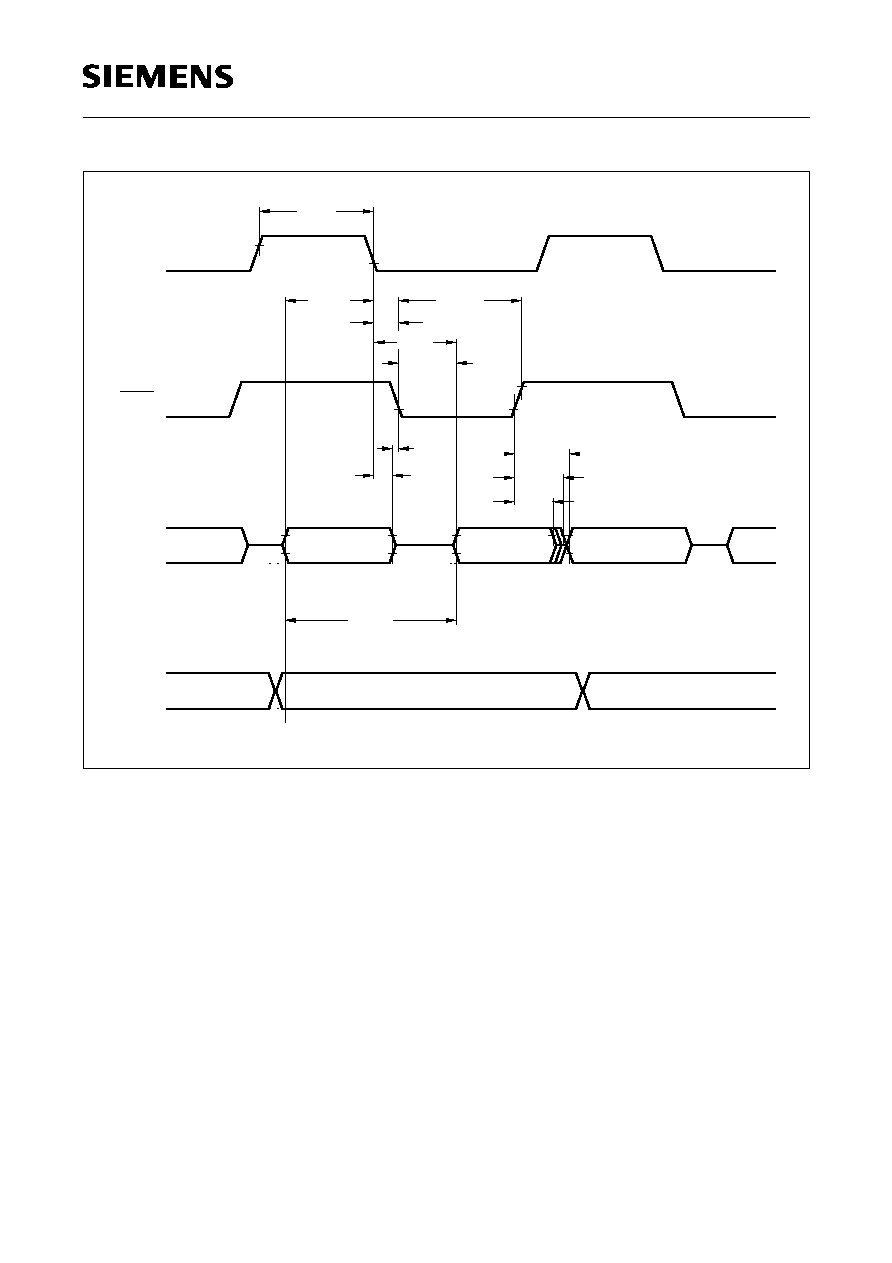
Semiconductor Group
61
1997-10-01
C517A
Figure 26
Program Memory Read Cycle
MCT00096
ALE
PSEN
Port 2
LHLL
t
A8 - A15
A8 - A15
A0 - A7
Instr.IN
A0 - A7
Port 0
t
AVLL
PLPH
t
t
LLPL
t
LLIV
t
PLIV
t
AZPL
t
LLAX
t
PXIZ
t
PXIX
t
AVIV
t
PXAV
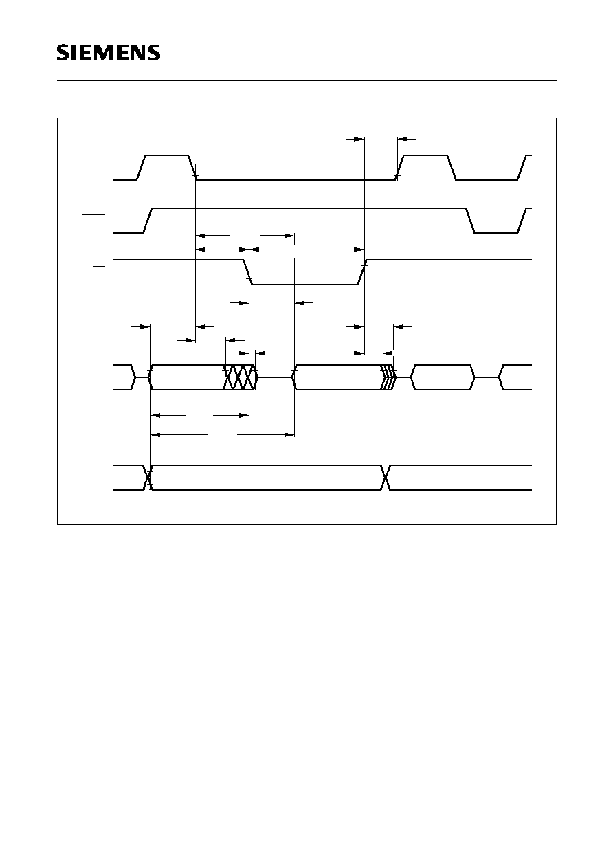
C517A
Semiconductor Group
62
1997-10-01
Figure 27
Data Memory Read Cycle
MCT00097
ALE
PSEN
Port 2
WHLH
t
Port 0
RD
t
LLDV
t
RLRH
t
LLWL
t
RLDV
t
AVLL
t
LLAX2
t
RLAZ
t
AVWL
t
AVDV
t
RHDX
t
RHDZ
A0 - A7 from
Ri or DPL
from PCL
A0 - A7
Instr.
IN
Data IN
A8 - A15 from PCH
P2.0 - P2.7 or A8 - A15 from DPH
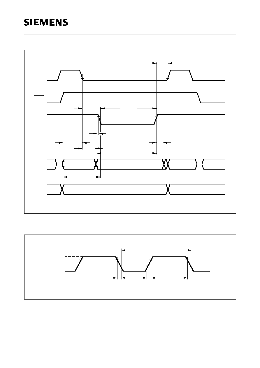
Semiconductor Group
63
1997-10-01
C517A
Figure 28
Data Memory Write Cycle
Figure 29
External Clock Drive on XTAL2
MCT00098
ALE
PSEN
Port 2
WHLH
t
Port 0
WR
t
WLWH
t
LLWL
t
QVWX
t
AVLL
t
LLAX2
t
QVWH
t
AVWL
t
WHQX
A0 - A7 from
Ri or DPL
from PCL
A0 - A7
Instr.IN
Data OUT
A8 - A15 from PCH
P2.0 - P2.7 or A8 - A15 from DPH
MCT00033
t
CHCX
t
CLCX
CHCL
t
CLCH
t
V
CC
t
CLCL
- 0.5V
0.45V
CC
0.7
V
V - 0.1
CC
0.2
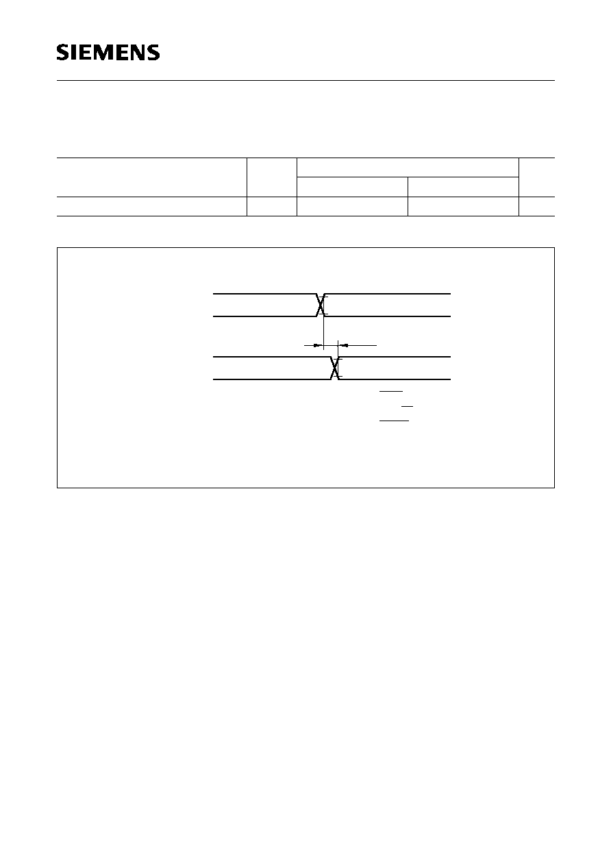
C517A
Semiconductor Group
64
1997-10-01
ROM Verification Characteristics for the C517A-1RM
ROM Verification Mode 1
Figure 30
ROM Verification Mode 1
Parameter
Symbol
Limit Values
Unit
min.
max.
Address to valid data
t
AVQV
≠
10
t
CLCL
ns
P1.0-P1.7
P2.0-P2.6
Port 0
MCS03253
Address
New Address
New Data Out
Data Out
t
AVQV
Data:
Addresses:
P0.0-P0.7
P1.0-P1.7
P2.0-P2.6
=
=
=
D0-D7
A0-A7
A8-A14
V
RESET
=
IL2
PSEN
Inputs:
=
=
ALE, EA
SS
V
V
IH
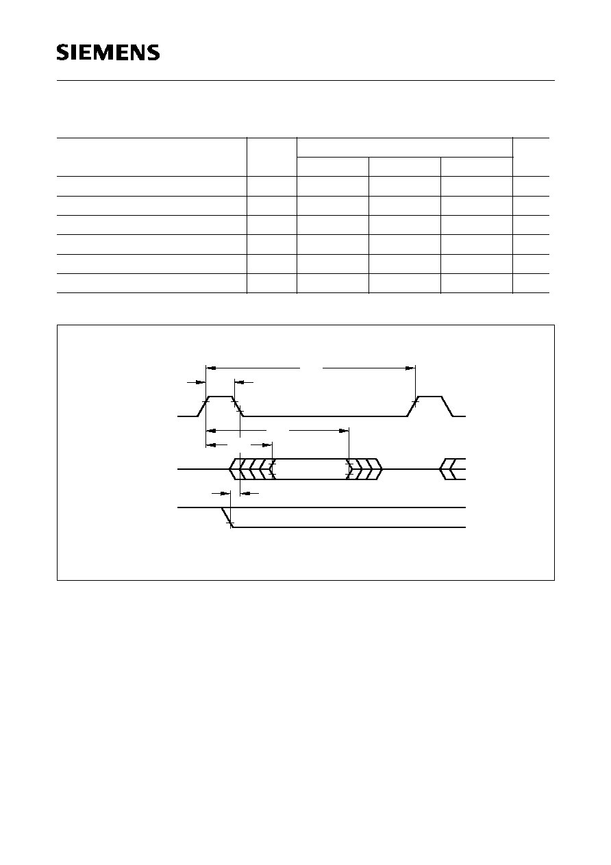
Semiconductor Group
65
1997-10-01
C517A
ROM Verification Mode 2
Figure 31
ROM Verification Mode 2
Parameter
Symbol
Limit Values
Unit
min.
typ
max.
ALE pulse width
t
AWD
≠
2
t
CLCL
≠
ns
ALE period
t
ACY
≠
12
t
CLCL
≠
ns
Data valid after ALE
t
DVA
≠
≠
4
t
CLCL
ns
Data stable after ALE
t
DSA
8
t
CLCL
≠
≠
ns
P3.5 setup to ALE low
t
AS
≠
t
CLCL
≠
ns
Oscillator frequency
1/
t
CLCL
3.5
≠
24
MHz
MCT02613
t
ACY
t
AWD
t
DSA
DVA
t
t
AS
Data Valid
ALE
Port 0
P3.5
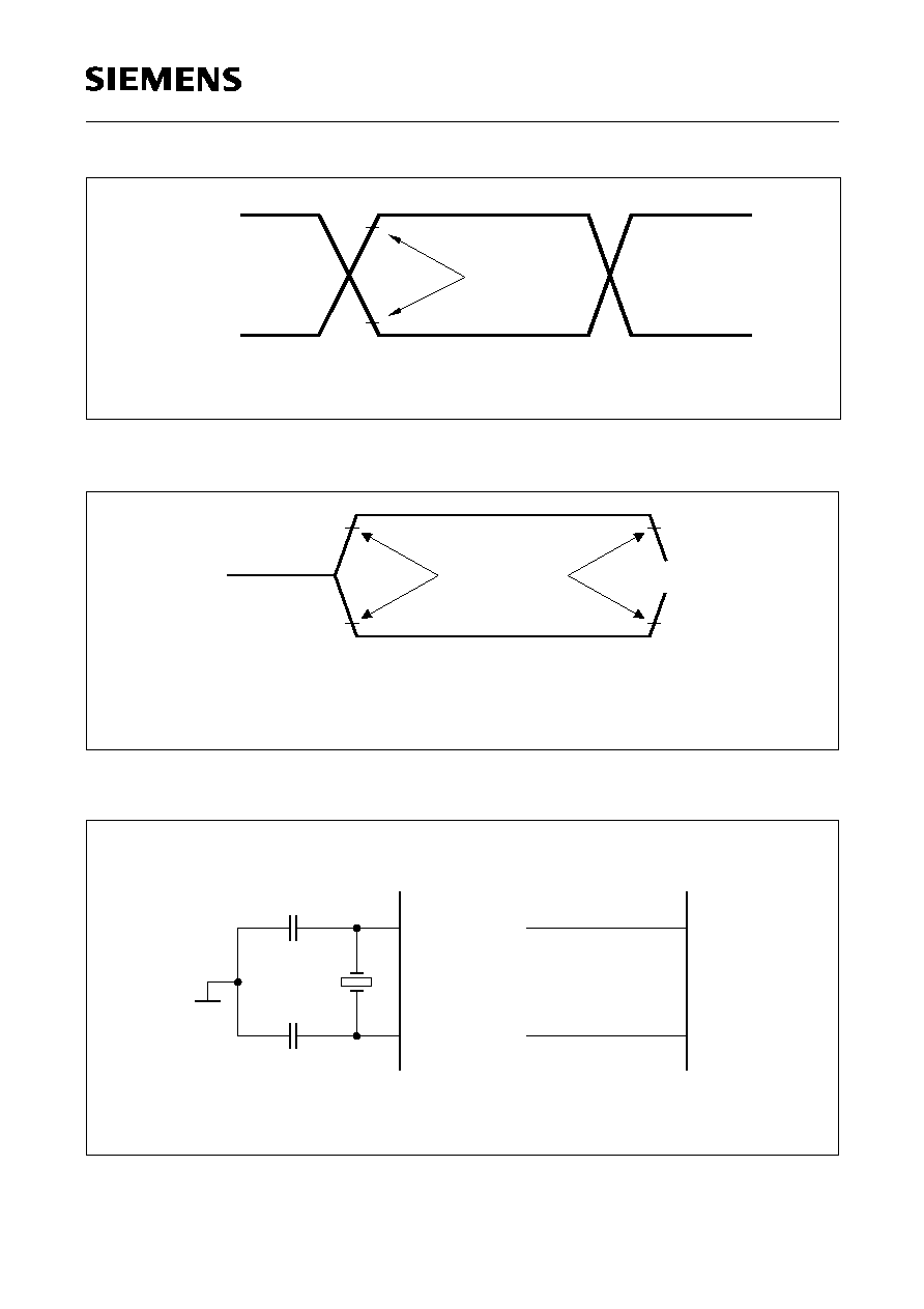
C517A
Semiconductor Group
66
1997-10-01
Figure 32
AC Testing: Input, Output Waveforms
Figure 33
AC Testing: Float Waveforms
Figure 34
Recommended Oscillator Circuits for Crystal Oscillator
AC Inputs during testing are driven at
V
CC
- 0.5 V for a logic '1' and 0.45 V for a logic '0'.
Timing measurements are made at
V
IHmin
for a logic '1' and
V
ILmax
for a logic '0'.
0.45 V
V
CC
0.2
-0.1
+0.9
0.2
CC
V
Test Points
MCT00039
V
CC
-0.5 V
For timing purposes a port pin is no longer floating when a 100 mV change from load voltage
occurs and begins to float when a 100 mV change from the loaded
V
OH
/
V
OL
level occurs.
I
OL
/
I
OH
±
20 mA
MCT00038
V
Load
V
Load
-0.1 V
+0.1 V
Load
V
Timing Reference
Points
V
OH
-0.1 V
+0.1 V
OL
V
3.5-24 MHz
XTAL1
XTAL2
= 20 pF
(incl. stray capacitance)
10 pF
±
Crystal Oscillator Mode
XTAL2
XTAL1
Driving from External Source
N.C.
External Oscillator
Signal
MCS03339
C
C
C
Crystal Mode :

Semiconductor Group
67
1997-10-01
C517A
Figure 35
P-MQFP-100-2 Package Outlines
GPM05623
Plastic Package, P-MQFP-100-2 (SMD)
(Plastic Metric Quad Flat Package)
Sorts of Packing
Package outlines for tubes, trays etc. are contained in our
Data Book "Package Information"
Dimensions in mm
SMD = Surface Mounted Device