
Semiconductor Group
1
NPN Silicon Switching Transistor
SMBT 3904
Maximum Ratings
Type
Ordering Code
(tape and reel)
Marking
Package
1)
Pin Configuration
SMBT 3904
Q68000-A4416
s1A
SOT-23
B
E
C
1
2
3
Parameter
Symbol
Values
Unit
Collector-emitter voltage
V
CE0
40
V
Collector-base voltage
V
CB0
60
Collector current
I
C
200
mA
Total power dissipation,
T
S
= 69 �C
P
tot
330
mW
Junction temperature
T
j
150
�C
Storage temperature range
T
stg
� 65 ... + 150
Thermal Resistance
Junction - ambient
2)
R
th JA
315
K/W
Junction - soldering point
R
th JS
245
Emitter-base voltage
V
EB0
6
1)
For detailed information see chapter Package Outlines.
2)
Package mounted on epoxy pcb 40 mm
�
40 mm
�
1.5 mm/6 cm
2
Cu.
q
High DC current gain: 0.1 mA to 100 mA
q
Low collector-emitter saturation voltage
q
Complementary type: SMBT 3906 (PNP)
5.91

Semiconductor Group
2
SMBT 3904
Electrical Characteristics
at
T
A
= 25 �C, unless otherwise specified.
Unit
Values
Parameter
Symbol
min.
typ.
max.
DC characteristics
V
Collector-emitter breakdown voltage
I
C
= 1 mA
V
(BR)CE0
40
�
�
Collector-base breakdown voltage
I
C
= 10
�
A
V
(BR)CB0
60
�
�
Emitter-base breakdown voltage
I
E
= 10
�
A
V
(BR)EB0
6
�
�
nA
Collector-base cutoff current
V
CB
= 30 V
I
CB0
�
�
50
�
DC current gain
I
C
= 100
�
A
, V
CE
= 1 V
I
C
= 1 mA,
V
CE
= 1 V
I
C
= 10 mA,
V
CE
= 1 V
1)
I
C
= 50 mA,
V
CE
= 1 V
1)
I
C
= 100 mA,
V
CE
= 1 V
1)
h
FE
40
70
100
60
30
�
�
�
�
�
�
�
300
�
�
V
Collector-emitter saturation voltage
1)
I
C
= 10 mA
, I
B
= 1 mA
I
C
= 50 mA
, I
B
= 5 mA
V
CEsat
�
�
�
�
0.2
0.3
Base-emitter saturation voltage
1)
I
C
= 10 mA
, I
B
= 1 mA
I
C
= 50 mA
, I
B
= 5 mA
V
BEsat
0.65
�
�
�
0.85
0.95
1)
Pulse test conditions:
t
300
�
s,
D
= 2 %.

Semiconductor Group
3
SMBT 3904
Electrical Characteristics
at
T
A
= 25 �C, unless otherwise specified.
dB
Noise figure
I
C
= 100
�
A
, V
CE
= 5 V,
R
S
= 1 k
,
f
= 1 kHz
F
�
�
5
MHz
Transition frequency
I
C
= 10 mA
, V
CE
= 20 V,
f
= 100 MHz
f
T
300
�
�
pF
Output capacitance
V
CB
= 5 V,
f
= 1 MHz
C
obo
�
�
4
AC characteristics
Unit
Values
Parameter
Symbol
min.
typ.
max.
Input capacitance
V
EB
= 0.5 V,
f
= 1 MHz
C
ibo
�
�
8
k
Input impedance
I
C
= 1 mA
, V
CE
= 10 V,
f
= 1 kHz
h
11e
1
�
10
10
� 4
Open-circuit reverse voltage transfer ratio
I
C
= 1 mA
, V
CE
= 10 V,
f
= 1 kHz
h
12e
0.5
�
8
�
Short-circuit forward current transfer ratio
I
C
= 1 mA
, V
CE
= 10 V,
f
= 1 kHz
h
21e
100
�
400
�
S
Open-circuit output admittance
I
C
= 1 mA
, V
CE
= 10 V,
f
= 1 kHz
h
22e
1
�
40
ns
ns
ns
ns
V
CC
= 3 V,
I
C
= 10 mA
, I
B1
= 1 mA
V
BE(off)
= 0.5 V
Delay time
Rise time
V
CC
= 3 V,
I
C
= 10 mA
, I
B1
=
I
B2
= 1 mA
Storage time
Fall time
(see diagrams)
t
d
t
r
t
stg
t
f
�
�
�
�
�
�
�
�
35
35
200
50
Semiconductor Group
4
SMBT 3904
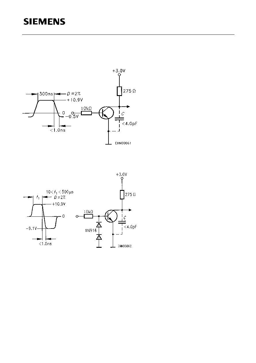
Test circuits
Delay and rise time
Storage and fall time
Semiconductor Group
5
SMBT 3904
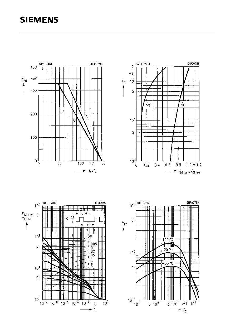
Total power dissipation
P
tot
=
f
(
T
A
*;
T
S
)
* Package mounted on epoxy
Permissible pulse load
P
tot max
/
P
tot DC
=
f
(
t
p
)
Saturation voltage
I
C
=
f
(
V
BE sat
,
V
CE sat
)
DC current gain
h
FE
=
f
(
I
C
)
V
CE
= 10 V, normalized
Semiconductor Group
6
SMBT 3904
Short-circuit forward current
transfer ratio
h
21e
=
f
(
I
C
)
V
CE
= 10 V,
f
= 1 MHz
Delay time
t
d
=
f
(
I
C
)
Rise time
t
r
=
f
(
I
C
)
Open-circuit output admittance
h
22e
=
f
(
I
C
)
V
CE
= 10 V,
f
= 1 MHz
Storage time
t
stg
=
f
(
I
C
)
Semiconductor Group
7
SMBT 3904
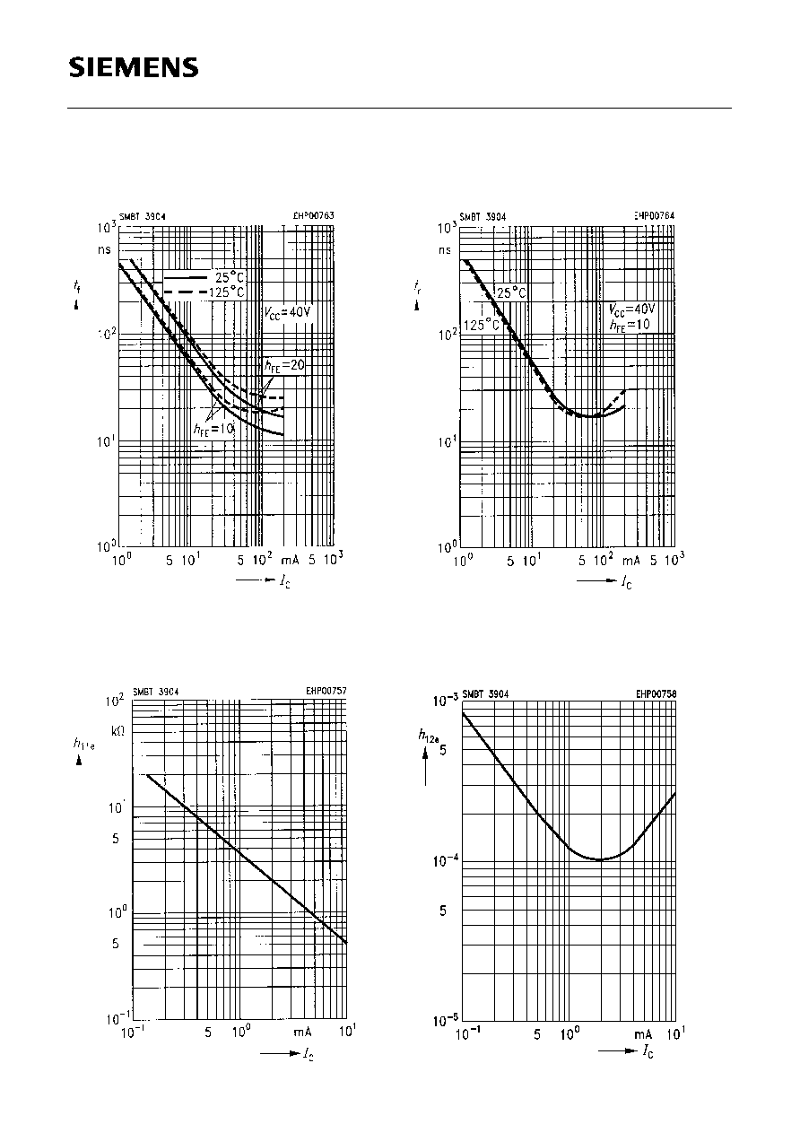
Fall time
t
f
=
f
(
I
C
)
Input impedance
h
11e
=
f
(
I
C
)
V
CE
= 10 V,
f
= 1 kHz
Rise time
t
r
=
f
(
I
C
)
Open-circuit reverse voltage
transfer ratio
h
12e
=
f
(
I
C
)
V
CE
= 10 V,
f
= 1 kHz