
Data Sheet 05.94
Microcomputer Components
SAB 80C517A/83C517A-5
8-Bit CMOS Single-Chip Microcontroller

Semiconductor Group
1
1994-05-01
High-Performance
SAB 80C517A/83C517A-5
8-Bit CMOS Single-Chip Microcontroller
Preliminary
SAB 83C517A-5
Microcontroller with factory mask-programmable ROM
SAB 80C517A
Microcontroller for external ROM
l
SAB 80C517A/83C517A-5,
l
Eight data pointers for external memory
up to 18 MHz operation
addressing
l
32 K
◊
8 ROM (SAB 83C517A-5 only,
l
Seventeen interrupt vectors, four priority
ROM-Protection available)
levels selectable
l
256
◊
8 on-chip RAM
l
Genuine 10-bit A/D converter with
l
2 K
◊
8 on-chip RAM (XRAM)
12 multiplexed inputs
l
Superset of SAB 80C51 architecture:
l
Two full duplex serial interfaces with
≠ 1
µ
s instruction cycle time at 12 MHz
programmable Baudrate-Generators
≠ 666 ns instruction cycle time at 18 MHz
l
Fully upward compatible with SAB 80C515,
≠ 256 directly addressable bits
SAB 80C517, SAB 80C515A
≠ Boolean processor
l
Extended power saving mode
≠ 64 Kbyte external data and
l
Fast Power-On Reset
program memory addressing
l
Nine ports: 56 I/O lines, 12 input lines
l
Four 16-bit timer/counters
l
Three temperature ranges available:
l
Powerful 16-bit compare/capture unit
0 to 70
o
C (T1)
(CCU) with up to 21 high-speed or PWM
≠ 40 to 85
o
C (T3)
output channels and 5 capture inputs
≠ 40 to 110
o
C (T4)
l
Versatile "fail-safe" provisions
l
Plastic packages: P-LCC-84,
l
Fast 32-bit division, 16-bit multiplication,
P-MQFP-100-2
32-bit normalize and shift by peripheral
MUL/DIV unit (MDU)
The SAB 80C517A/83C517A-5 is a high-end member of the Siemens SAB 8051 family of
microcontrollers. It is designed in Siemens ACMOS technology and based on SAB 8051
architecture. ACMOS is a technology which combines high-speed and density characteristics
with low-power consumption or dissipation.
While maintaining all the SAB 80C517 features and operating characteristics the
SAB 80C517A is expanded in its "fail-safe" characteristics and timer capabilities.The
SAB 80C517A is identical with the SAB 83C517A-5 except that it lacks the on-chip program
memory. The SAB 80C517A/83C517A-5 is supplied in a 84-pin plastic leaded chip carrier
package (P-LCC-84) and in a 100-pin plastic quad flat package (P-MQFP-100-2).
SAB 80C517A/83C517A-5
Semiconductor Group
2
1994-05-01
SAB 80C517A/83C517A-5
Revision History
05.94
Previous Releases
01.94/08.93/11.92/10.91/04.91
Page
Subjects (changes since last revision 04.91)
6
4
7-15
several
3
26, 27, 31
34
41
49
60
62
65
several
66
66
≠ Pin configuration P-MQFP-100-2 added
≠ Pin differences updated
≠ Pin numbers for P-MQFP-100-2 package added
≠ Correction of P-MRFP-100 into P-MQFP-100-2
≠ Ordering information for -40 to +110
∞
C versions
≠ Correction of register names S0RELL, SCON, ADCON, ICRON,
and SBUF
≠ Figure 4 corrected
≠ Figure 8 corrected
≠ PE/SWD function description completed
≠ Correct ordering numbers
≠ Test condition for
V
OH
,
V
OH1
corrected
≠
t
PXIZ
name corrected
t
AVIV,
t
AZPL
values corrected
≠ Minimum clock frequence is now 3.5 MHz
≠
t
QVWH
(data setup before WR) corrected and added
≠
t
LLAX2
corrected
Page
Subjects (changes since last revision 08.93)
26
51
65
65
74
≠ Corrected SFR name S0RELL
≠ Below "Termination of HWPD Mode": 4th paragraph with ident
corrected
≠ Description of
t
LLIV
corrected
≠ Program Memory Read Cycle:
t
PXAV
added
≠ Oscillator circuit drawings: MQFP-100-2 pin numbers added.
Page
Subjects (changes since last revision 01.94)
47
≠ Minor changes on several pages
≠ Table 6 corrected
SAB 80C517A/83C517A-5
Semiconductor Group
3
1994-05-01
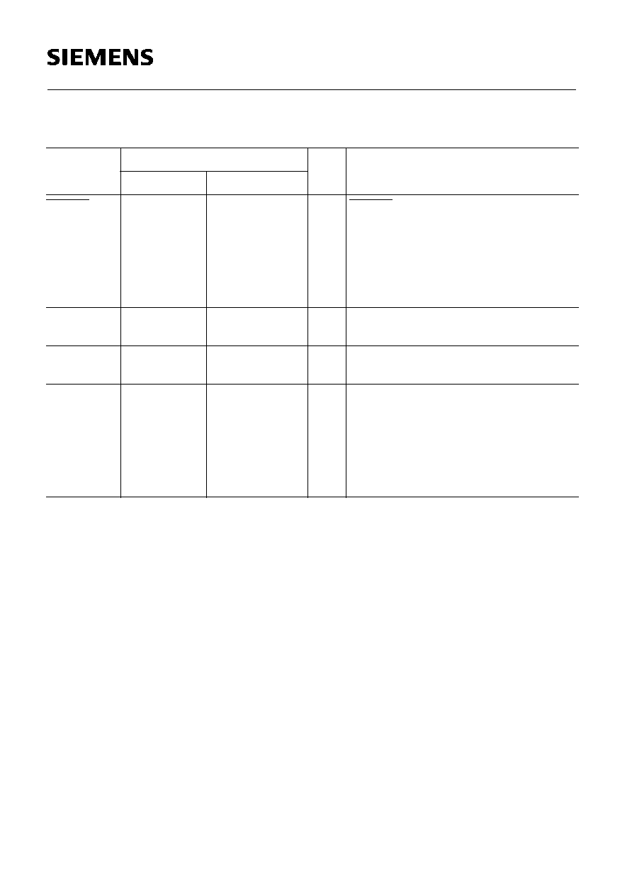
Ordering Information
Type
Ordering
Code
Package
Description
8-bit CMOS Microcontroller
SAB 80C517A-N18
Q67120-C583
P-LCC-84
for external memory,18 MHz
SAB 80C517A-M18
TBD
P-MQFP-100-2
SAB 83C517A-5N18
Q67120-C582
P-LCC-84
with mask-programmable ROM,
18 MHz
SAB 80C517A-N18-T3
Q67120-C769
P-LCC-84
for external memory,18 MHz
ext. temperature ≠ 40 to 85
o
C
SAB 83C517A-5N18-
T3
Q67120-C771
P-LCC-84
with mask-programmable ROM,
18 MHz
ext. temperature ≠ 40 to 85
o
C
SAB 83C517A-N18-T4
TBD
P-LCC-84
for external memory, 18 MHz
ext. temperature -40 to +110
o
C
SAB 83C517A-5N18-
T4
TBD
P-LCC-84
with mask-programmable ROM,
18 MHz
ext. temperature -40 to +110
o
C
SAB 80C517A/83C517A-5
Semiconductor Group
4
1994-05-01
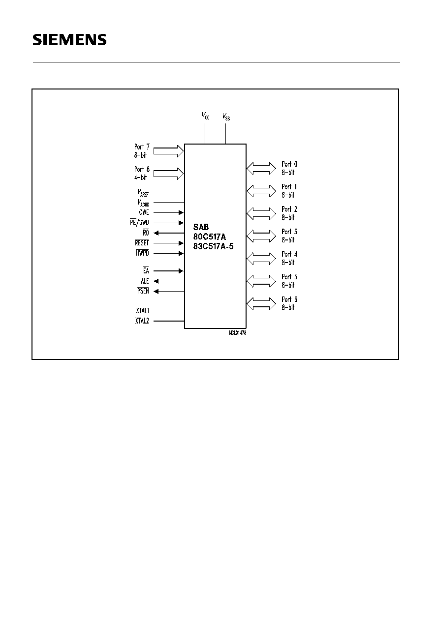
Logic Symbol
SAB 80C517A/83C517A-5
Semiconductor Group
5
1994-05-01
The pin functions of the SAB 80C517A are identical with those of the SAB 80C517/80C537 with
one exception:
Typ
SAB 80C517A
SAB 80C517/80C537
P-LCC-84, Pin 60
HWPD
N.C.
P-MQFP-100-2, Pin 36
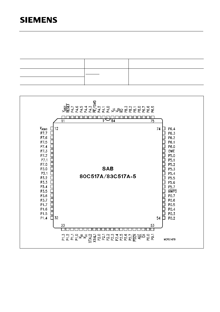
Pin Configuration
(P-LCC-84)

SAB 80C517A/83C517A-5
Semiconductor Group
6
1994-05-01
Pin Configuration
(P-MQFP-100-2)

SAB 80C517A/83C517A-5
Semiconductor Group
7
1994-05-01
Pin Definitions and Functions
Symbol
Pin Number
I/O
*)
Function
P-LCC-84
P-MQFP-100-2
P4.0 ≠ P4.7 1≠ 3, 5 ≠ 9
64 - 66,
68 - 72
I/O
Port 4
is a bidirectional I/O port with internal
pull-up resistors. Port 4 pins that have 1
s written to them are pulled high by the
internal pull-up resistors, and in that
state can be used as inputs. As inputs,
port 4 pins being externally pulled low
will source current (
I
IL,
in the DC char-
acteristics) because of the internal pull-
up resistors.
This port also serves alternate compare
functions. The secondary functions are
assigned to the pins of port 4 as follows:
≠ CM0 (P4.0): Compare Channel 0
≠ CM1 (P4.1): Compare Channel 1
≠ CM2 (P4.2): Compare Channel 2
≠ CM3 (P4.3): Compare Channel 3
≠ CM4 (P4.4): Compare Channel 4
≠ CM5 (P4.5): Compare Channel 5
≠ CM6 (P4.6): Compare Channel 6
≠ CM7 (P4.7): Compare Channel 7
PE/SWD
4
67
I
Power saving modes enable Start
Watchdog Timer
A low level on this pin allows the soft-
ware to enter the power down, idle and
slow down mode. In case the low level
is also seen during reset, the watchdog
timer function is off on default.
Use of the software controlled power
saving modes is blocked, when this pin
is held on high level. A high level during
reset performs an automatic start of the
watchdog timer immediately after reset.
When left unconnected this pin is pulled
high by a weak internal pull-up resistor.
*
I = Input
O = Output
SAB 80C517A/83C517A-5
Semiconductor Group
8
1994-05-01
Pin Definitions and Functions
(cont'd)
Symbol
Pin Number
I/O
*)
Function
P-LCC-84
P-MQFP-100-2
RESET
10
73
I
RESET
A low level on this pin for the duration of
one machine cycle while the oscillator is
running resets the SAB 80C517A. A
small internal pull-up resistor permits
power-on reset using only a capacitor
connected to
V
SS
.
V
AREF
11
78
Reference voltage
for the A/D con-
verter.
V
AGND
12
79
Reference ground
for the A/D
converter.
P7.7 -P7.0
13 - 20
80 - 87
I
Port 7
is an 8-bit unidirectional input port. Port
pins can be used for digital input, if
voltage levels meet the specified input
high/low voltages, and for the lower 8-
bit of the multiplexed analog inputs of
the A/D converter, simultaneously.
*
I = Input
O = Output
SAB 80C517A/83C517A-5
Semiconductor Group
9
1994-05-01
Pin Definitions and Functions
(cont'd)
Symbol
Pin Number
I/O
*)
Function
P-LCC-84
P-MQFP-100-2
P3.0 - P3.7 21 - 28
90 - 97
I/O
Port 3
is a bidirectional I/O port with internal pull-
up resistors. Port 3 pins that have 1 s
written to them are pulled high by the
internal pull-up resistors, and in that state
can be used as inputs. As inputs, port 3
pins being externally pulled low will source
current (
I
IL,
in the DC characteristics)
because of the internal pull-up resistors.
Port 3 also contains the interrupt, timer,
serial port 0 and external memory strobe
pins that are used by various options. The
output latch corresponding to a secondary
function must be programmed to a one (1)
for that function to operate.
The secondary functions are assigned to
the pins of port 3, as follows:
≠ R
◊
D0 (P3.0): receiver data input
(asynchronous) or data input/output
(synchronous) of serial interface
≠ T
◊
D0 (P3.1): transmitter data output
(asynchronous) or clock output
(synchronous) of serial interface 0
≠ INT0 (P3.2):
interrupt 0 input/timer 0
gate control
≠ INT1 (P3.3):
interrupt 1 input/timer 1
gate control
≠ T0 (P3.4):
counter 0 input
≠ T1 (P3.5):
counter 1 input
≠ WR (P3.6):
the write control signal
latches the data byte from port 0 into the
external data memory
≠ RD (P3.7):
the read control signal
enables the external data memory to
port 0
*
I = Input
O = Output

SAB 80C517A/83C517A-5
Semiconductor Group
10
1994-05-01
P1.7 - P1.0 29 - 36
98 - 100,
1, 6 - 9
I/O
Port 1
is a bidirectional I/O port with internal
pull-up resistors. Port 1 pins that have
1 s written to them are pulled high by the
internal pull-up resistors, and in that state
can be used as inputs. As inputs, port 1
pins being externally pulled low will source
current (
I
IL
, in the DC characteristics)
because of the internal pull-up resistors. It
is used for the low order address byte
during program verification. It also contains
the interrupt, timer, clock, capture and
compare pins that are used by various
options. The output latch must be
programmed to a one (1) for that function to
operate (except when used for the compare
functions).
The secondary functions are assigned to
the port 1 pins as follows:
≠ INT3/CC0 (P1.0): interrupt 3 input/
compare 0 output /capture 0 input
≠ INT4/CC1 (P1.1): interrupt 4 input /
compare 1 output /capture 1 input
≠ INT5/CC2 (P1.2): interrupt 5 input /
compare 2 output /capture 2 input
≠ INT6/CC3 (P1.3): interrupt 6 input /
compare 3 output /capture 3 input
≠ INT2/CC4 (P1.4): interrupt 2 input /
compare 4 output /capture 4 input
≠ T2EX (P1.5):
timer 2 external
reload trigger input
≠ CLKOUT (P1.6):
system clock output
≠ T2 (P1.7):
counter 2 input
*
I = Input
O = Output
Pin Definitions and Functions (cont'd)
Symbol
Pin Number
I/O
*)
Function
P-LCC-84
P-MQFP-100-2
SAB 80C517A/83C517A-5
Semiconductor Group
11
1994-05-01
XTAL2
39
12
≠
XTAL2
Input to the inverting oscillator amplifier and
input to the internal clock generator circuits.
XTAL1
40
13
≠
XTAL1
Output of the inverting oscillator amplifier.
To drive the device from an external clock
source, XTAL2 should be driven, while
XTAL1 is left unconnected. There are no
requirements on the duty cycle of the
external clock signal, since the input to the
internal clocking circuitry is devided down
by a divide-by-two flip-flop. Minimum and
maximum high and low times as well as
rise/fall times specified in the AC
characteristics must be observed.
P2.0 - P2.7 41 - 48
14 - 21
I/O
Port 2
is a bidirectional I/O port with internal pull-
up resistors. Port 2 pins that have 1 s
written to them are pulled high by the
internal pull-up resistors, and in that state
can be used as in-puts. As inputs, port 2
pins being externally pulled low will source
current (
I
IL
, in the DC characteristics)
because of the internal pull-up resistors.
Port 2 emits the high-order address byte
during fetches from external program
memory and during accesses to external
data memory that use 16-bit addresses
(MOVX @DPTR). In this application it uses
strong internal pull-up resistors when
issuing1 s. During accesses to external
data memory that use 8-bit addresses
(MOVX @Ri), port 2 issues the contents of
the P2 special function register.
*
I = Input
O = Output
Pin Definitions and Functions (cont'd)
Symbol
Pin Number
I/O
*)
Function
P-LCC-84
P-MQFP-100-2

SAB 80C517A/83C517A-5
Semiconductor Group
12
1994-05-01
PSEN
49
22
O
The Program Store Enable
output is a control signal that enables the
external program memory to the bus during
external fetch operations. It is activated
every six oscillator periodes except during
external data memory accesses. Remains
high during internal program execution.
ALE
50
23
O
The Address Latch Enable
output is used for latching the address into
external memory during normal operation.
It is activated every six oscillator periodes
except during an external data memory
access
EA
51
24
I
External Access Enable
When held at high level, instructions are
fetched from the internal ROM (SAB
83C517A-5 only) when the PC is less than
8000H. When held at low level, the SAB
80C517A fetches all instructions from ex-
ternal program memory. For the SAB
80C517A this pin must be tied low
P0.0 - P0.7 52 - 59
26 - 27,
30 - 35
I/O
Port 0
is an 8-bit open-drain bidirectional I/O port.
Port 0 pins that have 1 s written to them
float, and in that state can be used as high-
impe-dance inputs. Port 0 is also the
multiplexed low-order address and data
bus during accesses to external program or
data memory. In this application it uses
strong internal pull-up resistors when
issuing 1 s. Port 0 also out-puts the code
bytes during program verification in the
SAB 83C517A if ROM-Protection was not
enabled. External pull-up resistors are
required during program verification.
*
I = Input
O = Output
Pin Definitions and Functions (cont'd)
Symbol
Pin Number
I/O
*)
Function
P-LCC-84
P-MQFP-100-2

SAB 80C517A/83C517A-5
Semiconductor Group
13
1994-05-01
HWPD
60
36
I
Hardware Power Down
A low level on this pin for the duration of
one machine cycle while the oscillator is
running resets the SAB 80C517A. A low
level for a longer period will force the part to
Power Down Mode with the pins floating.
(see table 7)
P5.7 - P5.0 61 - 68
37 - 44
I/O
I
Port 5
is a bidirectional I/O port with internal pull-
up resistors. Port 5 pins that have 1 s
written to them are pulled high by the
internal pull-up resistors, and in that state
can be used as inputs. As inputs, port 5
pins being externally pulled low will source
current (
I
IL
, in the DC characteristics)
because of the internal pull-up resistors.
This port also serves the alternate function
"Concurrent Compare" and "Set/Reset
Compare". The secondary functions are
assigned to the port 5 pins as follows:
≠ CCM0 to CCM7 (P5.0 to P5.7):
concurrent compare or Set/Reset
OWE
69
45
I/O
Oscillator Watchdog Enable
A high level on this pin enables the
oscillator watchdog. When left
unconnected this pin is pulled high by a
weak internal pull-up resistor. When held at
low level the oscillator watchdog function is
off.
*
I = Input
O = Output
Pin Definitions and Functions (cont'd)
Symbol
Pin Number
I/O
*)
Function
P-LCC-84
P-MQFP-100-2
SAB 80C517A/83C517A-5
Semiconductor Group
14
1994-05-01
P6.0 - P6.7 70 - 77
46 - 50,
54 - 56
I/O
Port 6
is a bidirectional I/O port with internal pull-
up resistors. Port 6 pins that have 1 s
written to them are pulled high by the
internal pull-up resistors, and in that state
can be used as inputs. As inputs, port 6
pins being externally pulled low will source
current (
I
IL
, in the DC characteristics)
because of the internal pull-up resistors.
Port 6 also contains the external A/D
converter control pin and the transmit and
receive pins for serial channel 1. The
output latch corresponding to a secondary
function must be programmed to a one (1)
for that function to operate.
The secondary functions are assigned to
the pins of port 6, as follows:
≠ ADST (P6.0): external A/D converter
start pin
≠ R
◊
D1 (P6.1): receiver data input
of serial interface 1
≠ T
◊
D1 (P6.2): transmitter data output
of serial interface 1
P8.0 - P8.3 78 - 81
57 - 60
I
Port 8
is a 4-bit unidirectional input port. Port pins
can be used for digital input, if voltage
levels meet the specified input high/low
voltages, and for the higher 4-bit of the
multiplexed analog inputs of the A/D
converter, simultaneously
*
I = Input
O = Output
Pin Definitions and Functions (cont'd)
Symbol
Pin Number
I/O
*)
Function
P-LCC-84
P-MQFP-100-2

SAB 80C517A/83C517A-5
Semiconductor Group
15
1994-05-01
Pin Definitions and Functions (cont'd)
Symbol
Pin Number
I/O
*)
Function
P-LCC-84
P-MQFP-100-2
RO
82
61
O
Reset Output
This pin outputs the internally
synchronized reset request signal. This
signal may be generated by an external
hardware reset, a watchdog timer reset
or an oscillator watch-dog reset. The
reset output is active low.
V
S S
37, 83
10, 62
≠
Circuit ground potential
V
CC
38, 84
11, 63
≠
Supply Terminal for all operating
modes
N.C.
≠
2 - 5, 25,
28 - 29,
51 - 53,
74 - 77,
88 - 89
≠
Not connected
*
I = Input
O = Output

SAB 80C517A/83C517A-5
Semiconductor Group
16
1994-05-01
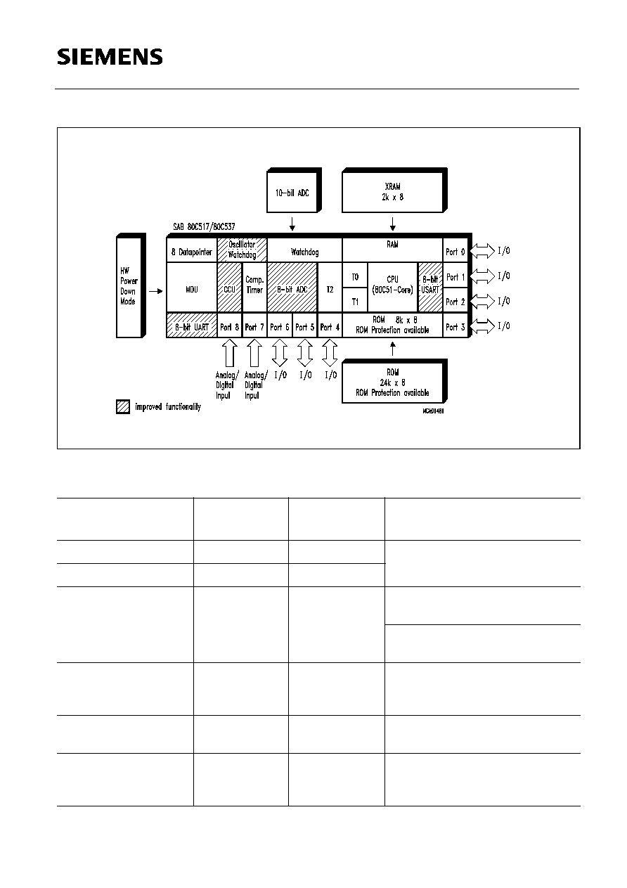
Figure 1
Block Diagram
SAB 80C517A/83C517A-5
Semiconductor Group
17
1994-05-01
Functional Description
The SAB 80C517A is based on 8051 architecture. It is a fully compatible member of the
Siemens SAB 8051/80C51 microcontroller family being an significantly enhanced
SAB 80C517. The SAB 80C517A is therefore compatible with code written for the
SAB 80C517.
Having an 8-bit CPU with extensive facilities for bit-handling and binary BCD arithmetics the
SAB 80C517A is optimized for control applications. With a 18 MHz crystal, 58 % of the
instructions are executed in 666.67 ns.
Being designed to close the performance gap to the 16-bit microcontroller world, the
SAB 80C517A's CPU is supported by a powerful 32-/16-bit arithmetic unit and a more flexible
addressing of external memory by eight 16-bit datapointers.
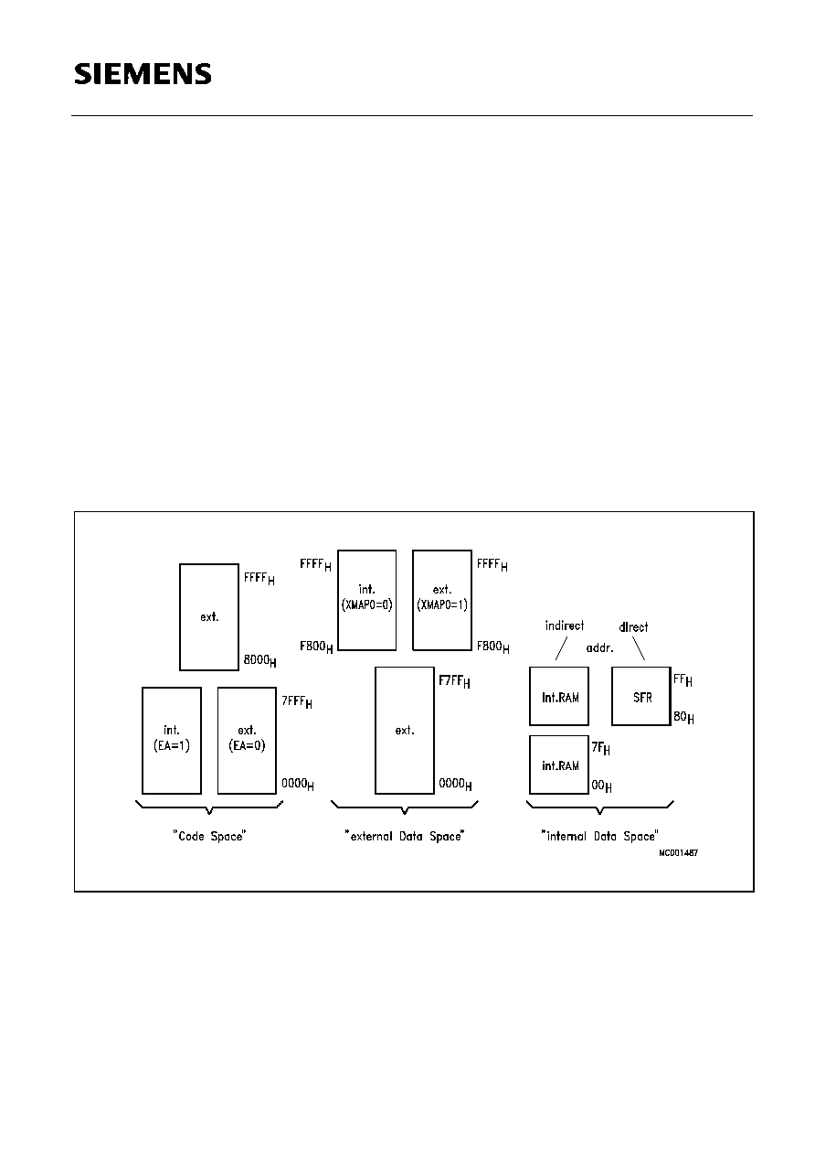
Memory Organisation
According to the SAB 8051 architecture, the SAB 80C517A has separate address spaces for
program and data memory. Figure 2 illustrates the mapping of address spaces.
Figure 2
Memory Map

SAB 80C517A/83C517A-5
Semiconductor Group
18
1994-05-01
Program Memory ('Code Space')
The SAB 83C517A-5 has 32 Kbyte of on-chip ROM, while the SAB 80C517A has no internal
ROM. The program memory can externally be expanded up to 64 Kbyte. Pin EA controls
whether program fetches below address 8000H are done from internal or external memory.
As a new feature the SAB 83C517A-5 offers the possibility of protecting the internal ROM
against unauthorized access. This protection is implemented in the ROM-Mask.Therefore, the
decision ROM-Protection 'yes' or 'no' has to be made when delivering the ROM-Code. Once
enabled, there is no way of disabling the ROM-Protection.
Effect:
The access to internal ROM done by an externally fetched MOVC instruction
is disabled. Nevertheless, an access from internal ROM to external ROM is possible.
To verify the read protected ROM-Code a special ROM-Verify-Mode is implemented. This
mode also can be used to verify unprotected internal ROM.
ROM -Protection
ROM-Verification Mode
(see 'AC Characteristics')
Restrictions
no
ROM-Verification Mode 1
(standard 8051 Verification Mode)
ROM-Verification Mode 2
≠
yes
ROM-Verification Mode 2
≠ standard 8051
Verification Mode is
disabled
≠ externally applied MOVC
accessing internal ROM
is disabled

SAB 80C517A/83C517A-5
Semiconductor Group
19
1994-05-01
Data Memory ('Code Space')
The data memory space consists of an internal and an external memory space. The
SAB 80C517A contains another 2 Kbyte on On-Chip RAM above the 256-bytes internal RAM
of the base type SAB 80C517. This RAM is called XRAM in this document.
External Data Memory
Up to 64 Kbyte external data memory can be addressed by instructions that use 8-bit or 16-bit
indirect addressing. For 8-bit addressing MOVX instructions in combination with registers R0
and R1 can be used. A 16-bit external memory addressing is supported by eight 16-bit
datapointers. Registers XPAGE and SYSCON are controlling whether data fetches at
addresses F800
H
to FFFF
H
are done from internal XRAM or from external data memory.
Internal Data Memory
The internal data memory is divided into four physically distinct blocks:
≠ the lower 128 bytes of RAM including four banks containing eight registers each
≠ the upper 128 byte of RAM
≠ the 128 byte special function register area.
≠ a 2 K
◊
8 area which is accessed like external RAM (MOVX-instructions), implemented on
chip at the address range from F800
H
to FFFF
H
. Special Function Register SYSCON
controls whether data is read or written to XRAM or external RAM.
A mapping of the internal data memory is also shown in figure 2. The overlapping address
spaces are accessed by different addressing modes (see User's Manual SAB 80C517). The
stack can be located anywhere in the internal data memory.
Architecture for the XRAM
The contents of the XRAM is not affected by a reset or HW Power Down. After power-up the
contents is undefined, while it remains unchanged during and after a reset or HW Power Down
if the power supply is not turned off.
The additional On-Chip RAM is logically located in the "external data memory" range at the
upper end of the 64 Kbyte address range (F800
H
-FFFF
H
). It is possible to enable and disable
(only by reset) the XRAM. If it is disabled the device shows the same behaviour as the parts
without XRAM, i.e. all MOVX accesses use the external bus to physically external data
memory.

SAB 80C517A/83C517A-5
Semiconductor Group
20
1994-05-01
Accesses to XRAM
Because the XRAM is used in the same way as external data memory the same instruction
types must be used for accessing the XRAM.
Note:
If a reset occurs during a write operation to XRAM, the effect on XRAM depends on the
cycle which the reset is detected at (MOVX is a 2-cycle instruction):
Reset detection at cycle 1:
The new value will not be written to XRAM. The old value
is not affected.
Reset detection at cycle 2:
The old value in XRAM is overwritten by the new value.
Accesses to XRAM using the DPTR
There are a Read and a Write instruction from and to XRAM which use one of the 16-bit DPTR
for indirect addressing. The instructions are:
MOVX A,
@DPTR (Read)
MOVX
@DPTR, A (Write)
Normally the use of these instructions would use a physically external memory. However, in the
SAB 80C517A the XRAM is accessed if it is enabled and if the DPTR points to the XRAM
address space (DPTR F800
H
).
Accesses to XRAM using the Registers R0/R1
The 8051 architecture provides also instructions for accesses to external data memory range
which use only an 8-bit address (indirect addressing with registers R0 or R1). The instructions
are:
MOVX A,
@Ri (Read)
MOVX
@Ri, A (Write)
In application systems, either a real 8-bit bus (with 8-bit address) is used or Port 2 serves as
page register which selects pages of 256-byte. However, the distinction, whether Port 2 is
used as general purpose I/O or as "page address" is made by the external system design. From
the device's point of view it cannot be decided whether the Port 2 data is used externally as
address or as I/O data!
Hence, a special page register is implemented into the SAB 80C517A to provide the possibility
of accessing the XRAM also with the MOVX @Ri instructions, i.e. XPAGE serves the same
function for the XRAM as Port 2 for external data memory.

SAB 80C517A/83C517A-5
Semiconductor Group
21
1994-05-01
Special Function Register XPAGE
The reset value of XPAGE is 00
H
.
XPAGE can be set and read by software.
The register XPAGE provides the upper address byte for accesses to XRAM with MOVX @Ri
instructions. If the address formed from XPAGE and Ri is less than the XRAM address range,
then an external access is performed. For the SAB 80C517A the contents of XPAGE must be
greater or equal than F8H in order to use the XRAM. Of course, the XRAM must be enabled if
it shall be used with MOVX @Ri instructions.
Thus, the register XPAGE is used for addressing of the XRAM; additionally its contents are
used for generating the internal XRAM select. If the contents of XPAGE is less than the XRAM
address range then an external bus access is performed where the upper address byte is
provided by P2 and not by XPAGE!
Therefore, the software has to distinguish two cases, if the MOVX @Ri instructions with paging
shall be used:
a) Access to XRAM:
The upper address byte must be written to XPAGE
or P2; both writes selects the XRAM address range.
b) Access to external memory: The upper address byte must be written to P2; XPAGE
will be loaded with the same address in order to deselect
the XRAM.
Addr. 91
H
XPAGE
SAB 80C517A/83C517A-5
Semiconductor Group
22
1994-05-01
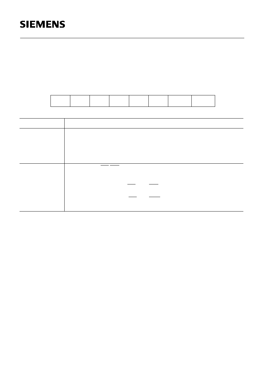
Control of XRAM in the SAB 80C517A
There are two control bits in register SYSCON which control the use and the bus operation
during accesses to the additional On-Chip RAM (XRAM).
Special Function Register SYSCON
Reset value of SYSCON is xxxx xx01B.
The control bit XMAP0 is a global enable/disable bit for the additional On-Chip RAM (XRAM).
If this bit is set, the XRAM is disabled, all MOVX accesses use external memory via the external
bus. In this case the SAB 80C517A does not use the additional On-Chip RAM and is compatible
with the types without XRAM.
Addr. 0B1
H
--
--
--
--
--
--
XMAP1
XMAP0
SYSCON
Bit
Function
XMAP0
Global enable/disable bit for XRAM memory.
XMAP0 = 0: The access to XRAM (= On-Chip XDATA memory) is en-
abled.
XMAP0 = 1: The access to XRAM is disabled. All MOVX accesses are per-
formed by the external bus (reset state).
XMAP1
Control bit for RD/WR signals during accesses to XRAM; this bit has no
effect if XRAM is disabled (XMAP0 = 1) or if addresses exceeding the
XRAM address range are used for MOVX accesses.
XMAP1 = 0: The signals RD and WR are not activated during accesses
to XRAM.
XMAP1 = 1: The signals RD and WR are activated during accesses to
XRAM.

SAB 80C517A/83C517A-5
Semiconductor Group
23
1994-05-01
XMAP0 is hardware protected by an unsymmetric latch. An unintentional disabling of XRAM
could be dangerous since indeterminate values would be read from external bus. To avoid this
the XMAP-bit is forced to '1' only by reset. Additionally, during reset an internal capacitor is
loaded. So after reset state XRAM is disabled. Because of the load time of the capacitor
XMAP0-bit once written to '0' (that is, discharging capacitor) cannot be set to '1' again by
software. On the other hand any distortion (software hang up, noise, ...) is not able to load this
capacitor, too. That is, the stable status is XRAM enabled. The only way to disable XRAM after
it was enabled is a reset.
The clear instruction for XMAP0 should be integrated in the program initialization routine before
XRAM is used. In extremely noisy systems the user may have redundant clear instructions.
The control bit XMAP1 is relevant only if the XRAM is accessed. In this case the externa RD
and WR signals at P3.6 and P3.7 are not activated during the access, if XMAP1 is cleared. For
debug purposes it might be useful to have these signals and the addresses at Ports 0.2
available. This is performed if XMAP1 is set.
The behaviour of Port 0 and P2 during a MOVX access depends on the control bits in register
SYSCON and on the state of pin EA. The table 1 lists the various operating conditions. It shows
the following characteristics:
a) Use of P0 and P2 pins during the MOVX access.
Bus: The pins work as external address/data bus. If (internal) XRAM is accessed, the
data written to the XRAM can be seen on the bus in debug mode.
I/0:
The pins work as Input/Output lines under control of their latch.
b) Activation of the RD and WR pin during the access.
c) Use of internal or external XDATA memory.
The shaded areas describe the standard operation as each 80C51 device without on-chip
XRAM behaves.
SAB 80C517A/83C517A-5
Semiconductor Group
24
1994-05-01
Table 1:
Behaviour of P0/P2 and
/
during MOVX accesses
RD WR
00
10
X1
DPTR < XRAM
address
range
MOVX
@Ri
MOVX
@DPTR
a) P0/P2
ð
Bus
b)
/
active
c) ext. memory is
used
RD WR
a) P0/P2
ð
Bus
b)
/
active
c) ext. memory is
used
RD WR
a) P0/P2
ð
Bus
b)
/
active
c) ext. memory is
used
RD WR
a) P0/P2
ð
Bus
b)
/
active
c) ext. memory is
used
RD WR
a) P0/P2
ð
Bus
b)
/
active
c) ext. memory is
used
RD WR
a) P0/P2
ð
Bus
b)
/
active
c) ext. memory is
used
RD WR
a) P0/P2
ð
Bus
b)
/
active
c) ext. memory is
used
RD WR
a) P0/P2
ð
Bus
b)
/
active
c) ext. memory is
used
RD WR
modes compatible to 8051 - family
00
10
X1
XMAP1, XMAP0
= 0
EA
a) P0/P2
ð
BUS
(
-Data only)
b)
/
inactive
c) XRAM is used
WR
RD WR
a) P0/P2
ð
BUS
(
-Data only)
b)
/
active
c) XRAM is used
WR
RD WR
a) P0/P2
ð
I/0
b)
/
inactive
c) XRAM is used
RD WR
a) P0/P2
ð
BUS
(
-Data only)
b)
/
active
c) XRAM is used
WR
RD WR
a) P0/P2
ð
BUS
(
-Data only)
P2
ð
I/0
b)
/
inactive
c) XRAM is used
WR
RD WR
a) P0/P2
ð
BUS
(
-Data only)
P2
ð
I/0
b)
/
active
c) XRAM is used
WR
RD WR
a) P0
ð
Bus
P2
ð
I/0
b)
/
active
c) ext. memory is
used
RD WR
a) P0/P2
ð
I/0
b)
/
inactive
c) XRAM is used
RD WR
a) P0
ð
BUS
(
-Data only)
P2
ð
I/0
b)
/
active
c) XRAM is used
WR
RD WR
a) P0
ð
Bus
P2
ð
I/0
b)
/
active
c) ext. memory is
used
RD WR
a) P0
ð
Bus
P2
ð
I/0
b)
/
active
c) ext. memory is
used
RD WR
a) P0
ð
Bus
P2
ð
I/0
b)
/
active
c) ext. memory is
used
RD WR
a) P0
ð
Bus
P2
ð
I/0
b)
/
active
c) ext. memory is
used
RD WR
a) P0
ð
Bus
P2
ð
I/0
b)
/
active
c) ext. memory is
used
RD WR
a) P0
ð
Bus
P2
ð
I/0
b)
/
active
c) ext. memory is
used
RD WR
DPTR
XRAM
address
range
XPAGE < XRAM
addr. page
range
XPAGE
XRAM
addr. page
range
XMAP1, XMAP0
= 1
EA
a) P0
ð
Bus
P2
ð
I/0
b)
/
active
c) ext. memory is
used
RD WR

SAB 80C517A/83C517A-5
Semiconductor Group
25
1994-05-01
Multiple Datapointers
As a functional enhancement to standard 8051 controllers, the SAB 80C517A contains eight
16-bit datapointers. The instruction set uses just one of these datapointers at a time. The
selection of the actual datapointer is done in special function register DPSEL (data pointer
select, addr. 92
H
). Figure 3 illustrates the addressing mechanism.
Figure 3
Addressing of External Data Memory
DPH(83 )
DPL(82 )
DPTR0
DPTR7
.0
.1
.2
-
-
-
-
-
DPSEL(92 )
DPSEL
Selected
Data-
pointer
.2
.1
.0
DPTR 0
0
0
0
0
0
1
DPTR 1
0
1
0
DPTR 2
0
1
1
DPTR 3
1
0
0
DPTR 4
1
0
1
DPTR 5
1
1
0
DPTR 6
1
1
1
DPTR 7
MCD00779
External Data Memory
H
H
H
SAB 80C517A/83C517A-5
Semiconductor Group
26
1994-05-01
Special Function Registers
All registers, except the program counter and the four general purpose register banks, reside
in the special function register area. The 81 special function registers include arithmetic
registers, pointers, and registers that provide an interface between the CPU and the on-chip
peripherals. There are also 128 directly addressable bits within the SFR area. All special
function registers are listed in table 1 and table 2.
In table 1 they are organized in numeric order of their addresses. In table 2 they are organized
in groups which refer to the functional blocks of the SAB 80C517A.
Table 2
Special Function Register
Address
Register
Contents
after Reset
Address
Register
Contents
after Reset
80
H
81
H
82
H
83
H
84
H
85
H
86
H
87
H
P0
1)
SP
DPL
DPH
(WDTL)
3)
(WDTH)
3)
WDTREL
PCON
FF
H
07
H
00
H
00
H
(00
H
)
(00
H
)
00
H
00
H
98
H
99
H
9A
H
9B
H
9C
H
9D
H
9E
H
9F
H
S0CON
1)
S0BUF
IEN2
S1CON
S1BUF
S1RELL
reserved
reserved
00
H
XX
H
XX00 00X0
B
0X00 0000
B
XX
H
00
H
XX
H
XX
H
88
H
89
H
8A
H
8B
H
8C
H
8D
H
8E
H
8F
H
TCON
1)
TMOD
TL0
TL1
TH0
TH1
reserved
reserved
00
H
00
H
00
H
00
H
00
H
00
H
XX
H
2)
XX
H
2)
A0
H
A1
H
A2
H
A3
H
A4
H
A5
H
A6
H
A7
H
P2
1)
COMSETL
COMSETH
COMCLRL
COMCLRH
SETMSK
CLRMSK
reserved
FF
H
00
H
00
H
00
H
00
H
00
H
00
H
XX
H
2
)
90
H
91
H
92
H
93
H
94
H
95
H
96
H
97
H
P1
1)
XPAGE
DPSEL
reserved
reserved
reserved
reserved
reserved
FF
H
00
H
XXXXX000B
XX
H
2
)
XX
H
2)
XX
H
2)
XX
H
2)
XX
H
2)
A8
H
A9
H
AA
H
AB
H
AC
H
AD
H
AE
H
AF
H
IEN0
1)
IP0
S0RELL
reserved
reserved
reserved
reserved
reserved
00
H
00
H
D9
H
XX
H
2
)
XX
H
2
)
XX
H
2
)
XX
H
2
)
XX
H
2
)
1)
Bit-addressable special function registers
2)
X means that the value is indeterminate and the location is reserved
3)
( )... SFRs not user accessable

SAB 80C517A/83C517A-5
Semiconductor Group
27
1994-05-01
Table 2
Special Function Register (cont'd)
Address
Register
Contents
after Reset
Address
Register
Contents
after Reset
B0
H
B1
H
B2
H
B3
H
B4
H
B5
H
B6
H
B7
H
P3
1)
SYSCON
reserved
reserved
reserved
reserved
reserved
reserved
FF
H
XXXX XX01B
XX
H
2
)
XX
H
2
)
XX
H
2
)
XX
H
2
)
XX
H
2
)
XX
H
2
)
D0
H
D1
H
D2
H
D3
H
D4
H
D5
H
D6
H
D7
H
PSW
1)
IRCON1
CML0
CMH0
CML1
CMH1
CML2
CMH2
00
H
00
H
00
H
00
H
00
H
00
H
00
H
00
H
B8
H
B9
H
BA
H
BB
H
BC
H
BD
H
BS
H
BF
H
IEN1
1)
IP1
S0RELH
S1RELH
reserved
reserved
reserved
reserved
00
H
XX00 0000B
XXXX XX11B
XXXX XX11B
XX
H
XX
H
XX
H
XX
H
D8
H
D9
H
DA
H
DB
H
DC
H
DD
H
DE
H
DF
H
ADCON0
1)
ADDATH
ADDATL
P7
ADCON1
P8
CTRELL
CTRELH
00
H
00
H
00
H
XX
H
XXXX0000
B
XX
H
00
H
00
H
C0
H
C1
H
C2
H
C3
H
C4
H
C5
H
C6
H
C7
H
IRCON0
1)
CCEN
CCL1
CCH1
CCL2
CCH2
CCL3
CCH3
00
H
00
H
00
H
00H
00
H
00
H
00
H
00
H
E0
H
E1
H
E2
H
E3
H
E4
H
E5
H
E6
H
E7
H
ACC
1)
CTCON
CML3
CMH3
CML4
CMH4
CML5
CMH5
00
H
0X00 0000
B
XX
H
00
H
00
H
00
H
00
H
00
H
C8
H
C9
H
CA
H
CB
H
CC
H
CD
H
CE
H
CF
H
T2CON
1)
CC4EN
CRCL
CRCH
TL2
TH2
CCL4
CCH4
00
H
00
H
00
H
00
H
00
H
00
H
00
H
00
H
E8
H
E9
H
EA
H
EB
H
EC
H
ED
H
EE
H
EF
H
P4
1)
MD0
MD1
MD2
MD3
MD4
MD5
ARCON
FF
H
XX
H
XX
H
XX
H
XX
H
XX
H
XX
H
0XXX XXXXB
1)
Bit-addressable special function registers
2)
X means that the value is indeterminate and the location is reserved
3)
( )... SFRs not user accessable

SAB 80C517A/83C517A-5
Semiconductor Group
28
1994-05-01
Table 2
Special Function Register (cont'd)
Address
Register
Contents
after Reset
Address
Register
Contents
after Reset
F0
H
F1
H
F2
H
F3
H
F4
H
F5
H
F6
H
F7
H
B
1)
reserved
CML6
CMH6
CML7
CMH7
CMEN
CMSEL
00
H
XX
H
00
H
00
H
00
H
00
H
00
H
00
H
F8
H
F9
H
FA
H
FB
H
FC
H
FD
H
FE
H
FF
H
P5
1)
reserved
P6
reserved
reserved
(IS0)
(IS1)
reserved
FF
H
XX
H
FF
H
XX
H
XX
H
XX
H
XX
H
XX
H
1)
Bit-addressable special function registers
2)
X means that the value is indeterminate and the location is reserved
3)
( )... SFRs not user accessable

SAB 80C517A/83C517A-5
Semiconductor Group
29
1994-05-01
Table 3
Special Function Registers - Functional Blocks
Block
Symbol
Name
Address
Contents
after Reset
CPU
ACC
B
DPH
DPL
DPSEL
PSW
SP
Accumulator
B-Register
Data Pointer, High Byte
Data Pointer, Low Byte
Data Pointer Select Register
Program Status Word Register
Stack Pointer
E0
H
1)
F0
H
1)
83
H
82
H
92
H
D0
H
1)
81
H
00
H
00
H
00
H
00
H
XXXX X000
B
3)
00
H
07
H
A/D-
Converter
ADCON0
ADCON1
ADDATH
ADDATL
A/D Converter Control Register 0
A/D Converter Control Register 1
A/D Converter Data Reg. High Byte
A/D Converter Data Reg. Low Byte
D8
H
1)
DC
H
D9
H
DA
H
00
H
00
H
00
H
00
H
Interrupt
System
IEN0
CTCON
2)
IEN1
IEN2
IP0
IP1
IRCON0
IRCON1
TCON
2)
TCON
2)
Interrupt Enable Register 0
Com. Timer Control Register
Interrupt Enable Register 1
Interrupt Enable Register 2
Interrupt Priority Register 0
Interrupt Priority Register 1
Interrupt Request Control Register
Interrupt Request Control Register
Timer Control Register
Timer 2 Control Register
A8
H
1)
E1
H
B8
H
1)
9A
H
A9
H
B9
H
C0
H
1)
D1
H
88
H
1)
C8
H
00
H
0XXX.0000
B
00
H
XXXX.00X0
B
3)
00
H
XX00 0000
B
00
H
00
H
00
H
00
H
MUL/DIV
Unit
ARCON
MD0
MD1
MD2
MD3
MD4
MD5
Arithmetic Control Register
Multiplication/Division Register 0
Multiplication/Division Register 1
Multiplication/Division Register 2
Multiplication/Division Register 3
Multiplication/Division Register 4
Multiplication/Division Register 5
EF
H
E9
H
EA
H
EB
H
EC
H
ED
H
EE
H
0XXXX XXXXB
XX
H
XX
H
XX
H
XX
H
XX
H
XX
H
1)
Bit-addressable special function registers
2)
This special function register is listed repeatedly since some bits of it also belong to other functional blocks.
3)
X means that the value is indeterminate and the location is reserved
SAB 80C517A/83C517A-5
Semiconductor Group
30
1994-05-01
Table 3
Special Function Registers - Functional Blocks (cont'd)
Block
Symbol
Name
Address
Contents
after Reset
Compare/
Capture-
Unit
(CCU)
Timer 2
CCEN
CC4EN
CCH1
CCH2
CCH3
CCH4
CCL1
CCL2
CCL3
CCL4
CMEN
CMH0
CMH1
CMH2
CMH3
CMH4
CMH5
CMH6
CMH7
CML0
CML1
CML2
CML3
CML4
CML5
CML6
CML7
CMSEL
CRCH
CRCL
COMSETL
COMSETH
COMCLRL
COMCLRH
SETMSK
Comp./Capture Enable Reg.
Comp./Capture Enable 4 Reg.
Comp./Capture Reg. 1, High Byte
Comp./Capture Reg. 2, High Byte
Comp./Capture Reg. 3, High Byte
Comp./Capture Reg. 4, High Byte
Comp./Capture Reg. 1, Low Byte
Comp./Capture Reg. 2, Low Byte
Comp./Capture Reg. 3, Low Byte
Comp./Capture Reg. 4, Low Byte
Compare Enable Register
Compare Register 0, High Byte
Compare Register 1, High Byte
Compare Register 2, High Byte
Compare Register 3, High Byte
Compare Register 4, High Byte
Compare Register 5, High Byte
Compare Register 6, High Byte
Compare Register 7, High Byte
Compare Register 0, Low Byte
Compare Register 1, Low Byte
Compare Register 2, Low Byte
Compare Register 3, Low Byte
Compare Register 4, Low Byte
Compare Register 5, Low Byte
Compare Register 6, Low Byte
Compare Register 7, Low Byte
Compare Input Select
Com./Rel./Capt. Reg. High Byte
Com./Rel./Capt. Reg. Low Byte
Compare Register, Low Byte
Compare Register, High Byte
Compare Register, Low Byte
Compare Register, High Byte
Mask Register, concerning
COMSET
C1
H
C9
H
C3
H
C5
H
C7
H
CF
H
C2
H
C4
H
C6
H
CE
H
F6
H
D3
H
D5
H
D7
H
E3
H
E5
H
E7
H
F3
H
F5
H
D2
H
D4
H
D6
H
E2
H
E4
H
E6
H
F2
H
F4
H
F7
H
CB
H
CA
H
A1
H
A2
H
A3
H
A4
H
A5
H
00
H
00
H
00
H
00
H
00
H
00
H
00
H
00
H
00
H
00
H
00
H
00
H
00
H
00
H
00
H
00
H
00
H
00
H
00
H
00
H
00
H
00
H
00
H
00
H
00
H
00
H
00
H
00
H
00
H
00
H
00
H
00
H
00
H
00
H
00
H
1)
Bit-addressable special function registers
2)
This special function register is listed repeatedly since some bits of it also belong to other functional blocks.
3)
X means that the value is indeterminate and the location is reserved

SAB 80C517A/83C517A-5
Semiconductor Group
31
1994-05-01
Compare/
Capture-
Unit
(CCU),
(cont'd)
CLRMSK
CTCON
CTRELH
CTRELL
TH2
TL2
T2CON
Mask Register, concerning
COMCLR
Com. Timer Control Reg.
Com. Timer Rel. Reg., High Byte
Com. Timer Rel. Reg., Low Byte
Timer 2, High Byte
Timer 2, Low Byte
Timer 2 Control Register
A6
H
E1
H
DF
H
DE
H
CD
H
CC
H
C8
H
1)
00
H
0X00 0000
B
3)
00
H
00
H
00
H
00
H
00
H
Ports
P0
P1
P2
P3
P4
P5
P6
P7
P8
Port 0
Port 1
Port 2
Port 3
Port 4
Port 5
Port 6,
Port 7, Analog/Digital Input
Port 8, Analog/Digital Input, 4-bit
80
H
1)
90
H
1)
A0
H
1)
B0
H
1)
E8
H
1)
F8
H
1)
FA
H
DB
H
DD
H
FF
H
FF
H
FF
H
FF
H
FF
H
FF
H
FF
H
Pow.Sav.
Modes
PCON
Power Control Register
87
H
00
H
Serial
Channels
ADCON0
2)
PCON
2)
S0BUF
S0CON
S0RELL
S0RELH
S1BUF
S1CON
S1REL
S1RELH
A/D Converter Control Reg.
Power Control Register
Serial Channel 0 Buffer Reg.
Serial Channel 0 Control Reg.
Serial Channel 0, Reload Reg., low
byte
Serial Channel 0, Reload Reg., high
byte
Serial Channel 1 Buffer Reg.,
Serial Channel 1 Control Reg.
Serial Channel 1 Reload Reg.,
low byte
Serial Channel 1 Reload Reg.,
high byte
D8
H
1)
87
H
99
H
98
H
1)
B2
H
BA
H
9C
H
9B
H
9D
H
BB
H
00
H
00
H
XX
H
3)
00
H
0D9
H
XXXX.XX11
B
3)
0XX
H
3)
0X00.0000
B
3)
00
H
XXXX.XX11
B
3)
1)
Bit-addressable special function registers
2)
This special function register is listed repeatedly since some bits of it also belong to other functional blocks.
3)
X means that the value is indeterminate and the location is reserved
Table 3
Special Function Registers - Functional Blocks (cont'd)
Block
Symbol
Name
Address
Contents
after Reset
SAB 80C517A/83C517A-5
Semiconductor Group
32
1994-05-01
Timer 0/
Timer 1
TCON
TH0
TH1
TL0
TL1
TMOD
Timer Control Register
Timer 0, High Byte
Timer 1, High Byte
Timer 0, Low Byte
Timer 1, Low Byte
Timer Mode Register
88
H
1)
8C
H
8D
H
8A
H
8B
H
89
H
00
H
00
H
00
H
00
H
00
H
00
H
Watchdog
IEN0
2)
IEN1
2)
IP0
2)
IP1
2)
WDTREL
Interrupt Enable Register 0
Interrupt Enable Register 1
Interrupt Priority Register 0
Interrupt Priority Register 1
Watchdog Timer Reload Reg.
A8
H
1)
B8
H
1)
A9
H
B9
H
86
H
00
H
00
H
00
H
XX00 0000
B
3)
00
H
1)
Bit-addressable special function registers
2)
This special function register is listed repeatedly since some bits of it also belong to other functional blocks.
3)
X means that the value is indeterminate and the location is reserved
Table 3
Special Function Registers - Functional Blocks (cont'd)
Block
Symbol
Name
Address
Contents
after Reset
SAB 80C517A/83C517A-5
Semiconductor Group
33
1994-05-01
A/D Converter
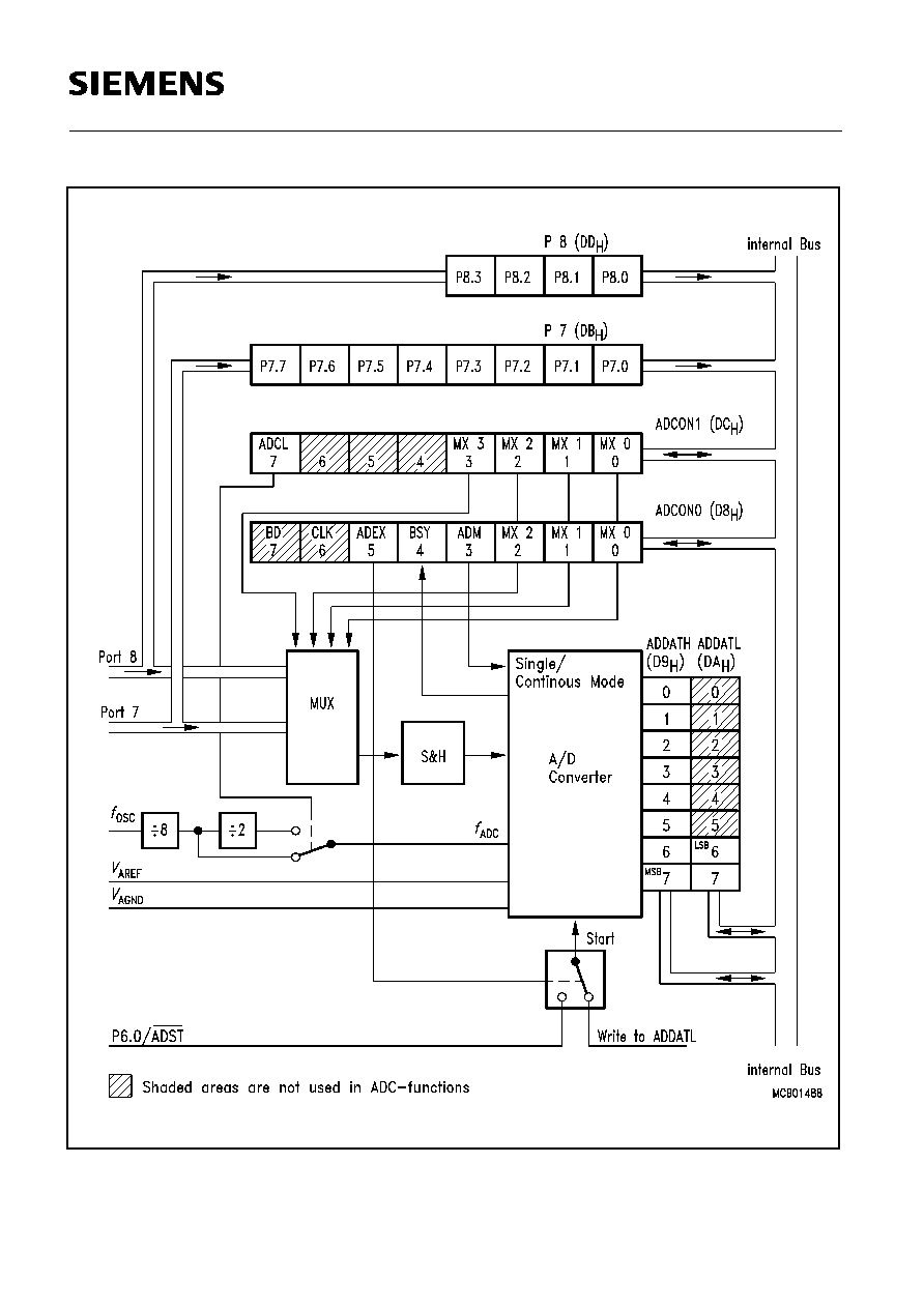
In the SAB 80C517A a new high performance / high-speed 12-channel 10-bit A/D-Converter is
implemented. Its successive approximation technique provides 7
µ
s con-version time (
f
OSC
= 16
MHz). The conversion principle is upward compatible to the one used in the SAB 80C517. The
main functional blocks are shown in figure 4.
The comparator is a fully differential comparator for a high power supply rejection ratio and very
low offset voltages. The capacitor network is binary weighted providing genuine 10-bit
resolution.
The table below shows the sample time
T
S
and the conversion time
T
C
, which are dependend
on
f
OSC
and a new prescaler (see also Bit ADCL in SFR ADCON 1).
f
OSC
[MHz]
Prescaler
f
ADC
[MHz]
Sample Time
T
S
[
µ
s]
Conversion Time
(incl. sample time)
T
C
[
µ
s]
12
˜
8
1.5
2.67
9.33
˜
16
0.75
5.33
18.66
16
˜
8
2.0
2.0
7.0
˜
16
1.0
4.0
14.0
18
˜
8
≠
≠
≠
˜
16
1.125
3.55
12.4
SAB 80C517A/83C517A-5
Semiconductor Group
34
1994-05-01
Figure 4
Block Diagram A/D Converter

SAB 80C517A/83C517A-5
Semiconductor Group
35
1994-05-01
Compare/Capture Unit (CCU)
The compare/capture unit is a complex timer/register array for applications that require high
speed I/O pulse width modulation and more timer/counter capabilities.
The CCU contains
≠ one 16-bit timer/counter (timer2) with 2-bit prescaler, reload capability and a max. clock
frequency of
f
OSC/12
(1 MHz with a 12 MHz crystal).
≠ one 16-bit timer (compare timer) with 8-bit prescaler, reload capability and a max. clock
frequency of
f
OSC/2
(6 MHz with a 12 MHz crystal).
≠ fifteen 16-bit compare registers.
≠ five of which can be used as 16-bit capture registers.
≠ up to 21 output lines controlled by the CCU.
≠ nine interrupts which can be generated by CCU-events.
Figure 5 shows a block diagram of the CCU. Eight compare registers (CM0 to CM7) can
individually be assigned to either timer 2 or the compare timer. Diagrams of the two timers are
shown in figures 6 and 7. The four compare/capture registers, the compare/reload/capture
register and the comset/comclr register are always connected to timer 2. Depending on the
register type and the assigned timer three different compare modes can be selected.
Table 3 illustrates possible combinations and the corresponding output lines.
SAB 80C517A/83C517A-5
Semiconductor Group
36
1994-05-01
Table 4
CCU Compare Configuration
Assigned Timer Compare Register
Compare Output
Possible Modes
Timer 2
CRCH/CRCL
CC1H/CC1L
CC2H/CC2L
CC3H/CC3L
CC4H/CC4L
CC4H/CC4L
:
CC4H/CC4L
COMSETL/COMSETH
COMCLRL/
COMCLRH
CM0H/CM0L
:
CM7H/CM7L
P1.0/INT3/CC0
P1.1/INT4/CC1
P1.2/INT5/CC2
P1.3/INT6/CC3
P1.4/INT2/CC4
P5.0/CCM0
:
P5.7/CCM7
P5.0/CCM0
:
P5.7/CCM7
P5.0/CCM0
:
P5.7/CCM7
P4.0/CM0
:
P4.7/CM7
Comp. mode 0, 1 + Reload
Comp. mode 0, 1
Comp. mode 0, 1
Comp. mode 0, 1
Comp. mode 0, 1
Comp. mode 1
:
Comp. mode 1
Comp. mode 2
:
Comp. mode 2
Comp. mode 2
:
Comp. mode 2
Comp. mode 1
:
Comp. mode 1
Compare
timer
CM0H/CM0L
:
CM7H/CM7L
P4.0/CM0
:
P4.7/CM7
Comp. mode 0
(with shadow latches)
:
Comp. mode 0
(with shadow latches)
SAB 80C517A/83C517A-5
Semiconductor Group
37
1994-05-01
Figure 5
Block Diagram of the Compare/Capture Unit

SAB 80C517A/83C517A-5
Semiconductor Group
38
1994-05-01
Compare
In compare mode, the 16-bit values stored in the dedicated compare registers are compared
to the contents of the timer 2 register or the compare timer register. If the count value in the
timer registers matches one of the stored value, an appropriate output signal is generated at
the corresponding pin(s) and an interrupt is requested. Three compare modes are provided:
Mode 0:
Upon a match the output signal changes from low to high.
It returns to low level at timer overflow.
Mode 1: The transition of the output signal can be determined by software.
A timer overflow signal does not affect the compare-output.
Mode 2:
In compare mode 2 the concurrent compare output pins on Port 5 are used
as follows (see figure 9)
≠ When a compare match occurs with register COMSET, a high level
appears at the pins of port 5 whose corresponding bits in the mask
register SETMSK (address 0A5
H
) are set.
≠ When a compare match occurs in register COMCLR, a low level
appears at the pins of port 5 whose corresponding bits in the mask
register CLRMSK (address 0A6
H
) are set.
Additionally the Port 5 pins used for compare mode 2 may also be
directly written to by write instructions to SFR P5. Of course, the pins
can also be read under program control.
Compare registers CM0 to CM7 use additional compare latches when operated in mode 0.
Figure 8 shows the function of these latches. The latches are implemented to prevent from loss
of compare matches which may occur when loading of the compare values is not correlated
with the timer count. The compare latches are automatically loaded from the compare registers
at every timer overflow.
Capture
This feature permits saving of the actual timer/counter contents into a selected register upon
an external event or a software write operation. Two modes are provided to 'freeze' the current
16-bit value of timer 2 registers into a dedicated capture register.
Mode 0:
Capture is performed in response to a transition at the corresponding
port 1 pins CC0 to CC3.
Mode 1:
Write operation into the low-order byte of the dedicated capture register
causes the timer 2 contents to be latched into this register.

SAB 80C517A/83C517A-5
Semiconductor Group
39
1994-05-01
Reload of Timer 2
A 16-bit reload can be performed with the 16-bit CRC register, which is a concatenation of the
8-bit registers CRCL and CRCH. There are two modes from which to select:
Mode 0:
Reload is caused by a timer overflow (auto-reload).
Mode 1:
Reload is caused in response to a negative transition at pin T2EX (P1.5),
which can also request an interrupt.
Timer/Counters 0 and 1
These timer/counters are fully compatible with timer/counter 0 or 1 of the SAB 8051 and can
operate in four modes:
Mode 0:
8-bit timer/counter with 32:1 prescaler
Mode 1:
16-bit timer/counter
Mode 2:
8-bit timer/counter with 8-bit auto reload
Mode 3:
Timer/counter 0 is configured as one 8-bit timer;
timer/counter 1 in this mode holds its count.
External inputs INT0 and INT1 can be programmed to function as a gate for timer/counters
0 and 1 to facilitate pulse width measurements.

SAB 80C517A/83C517A-5
Semiconductor Group
40
1994-05-01
Figure 6
Block Diagram of Timer 2

SAB 80C517A/83C517A-5
Semiconductor Group
41
1994-05-01
Figure 7
Block Diagram of the Compare Timer
Figure 8
Compare-Mode 0 with Registers CM0 to CM7
16-Bit Reload (CTREL)
16-Bit Compare Timer
Control (CTCON)
CTF
Overflow
To Interrupt
Circuitry
To Compare
Circuitry
16
3-Bit Prescaler
/2
/4
/8
/16
/32
/64
/128
Compare Timer
f
OSC
/2
MCB00783
SAB 80C517A/83C517A-5
Semiconductor Group
42
1994-05-01
Figure 9
Compare-Mode 2 (Port 5 only)
SAB 80C517A/83C517A-5
Semiconductor Group
43
1994-05-01
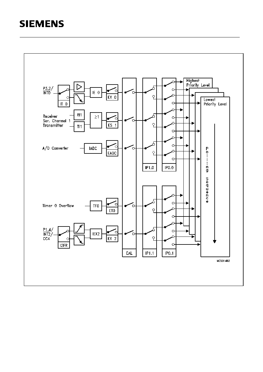
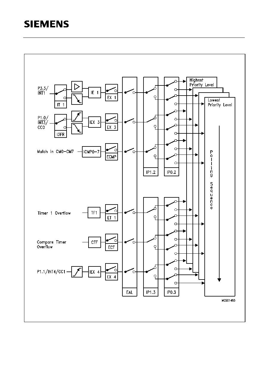
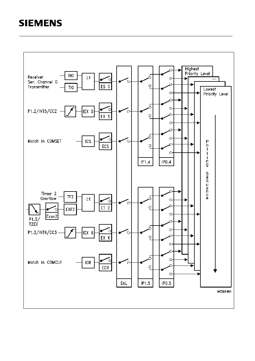
Interrupt Structure
The SAB 80C517A has 17 interrupt vectors with the following vector addresses and request
flags.
Each interrupt vector can be individually enabled/disabled. The response time to an interrupt
request is more than 3 machine cycles and less than 9 machine cycles.
External interrupts 0 and 1 can be activated by a low-level or a negative transition (selectable)
at their corresponding input pin, external interrupts 2 and 3 can be programmed for triggering
on a negative or a positive transition. The external interrupts 2 to 6 are combined with the
corresponding alternate functions compare (output) and capture (input) on port 1.
For programming of the priority levels the interrupt vectors are combined to pairs or triples.
Each pair or triple can be programmed individually to one of four priority levels by setting or
clearing one bit in special function register IP0 and one in IP1. Figure 9 shows the interrupt
request sources, the enabling and the priority level structure.
Table 5
Interrupt Sources and Vectors
Interrupt Request Flags
Interrupt Vector Address
Interrupt Source
IE0
TF0
IE1
TF1
RI0 + TI0
TF2 + EXF2
IADC
IEX2
IEX3
IEX4
IEX5
IEX6
RI1/TI1
ICMP0 to ICMP7
CTF
ICS
ICR
0003
H
000B
H
0013
H
001B
H
0023
H
002B
H
0043
H
004B
H
0053
H
005B
H
0063
H
006B
H
0083
H
0093
H
009B
H
00A3
H
00AB
H
External interrupt 0
Timer 0 overflow
External interrupt 1
Timer 1 overflow
Serial channel 0
Timer 2 overflow/ext. reload
A/D converter
External interrupt 2
External interrupt 3
External interrupt 4
External interrupt 5
External interrupt 6
Serial channel 1
Compare match interrupt of
Compare Registers CM0-
CM7 assigned to Timer 2
Compare timer overflow
Compare match interrupt of
Compare Register COMSET
Compare match interrupt of
Compare Register COMCLR
SAB 80C517A/83C517A-5
Semiconductor Group
44
1994-05-01
Figure 10
Interrupt Structure of the SAB 80C517A
SAB 80C517A/83C517A-5
Semiconductor Group
45
1994-05-01
Figure 10
Interrupt Structure of the SAB 80C517A (cont'd)
SAB 80C517A/83C517A-5
Semiconductor Group
46
1994-05-01
Figure 10
Interrupt Structure of the SAB 80C517A (cont'd)

SAB 80C517A/83C517A-5
Semiconductor Group
47
1994-05-01
Multiplication/Division Unit
This on-chip arithmetic unit provides fast 32-bit division, 16-bit multiplication as well as shift
and normalize features. All operations are integer operation.
The MDU consists of six registers used for operands and results and one control register.
Operation of the MDU can be divided in three phases:
Operation of the MDU
To start an operation, register MD0 to MD5 (or ARCON) must be written to in a certain se-
quence according to table 5 or 6. The order the registers are accessed determines the type of
the operation. A shift operation is started by a final write operation to register ARCON (see also
the register description).
Operation
Result
Remainder
Execution Time
32-bit/16-bit
32-bit
16-bit
6
t
cy
1)
16-bit/16-bit
16-bit
16-bit
4
t
cy
16-bit
*
16-bit
32-bit
≠
4
t
cy
32-bit normalize
≠
≠
6
t
cy
2)
32-bit shift left/right
≠
≠
6
t
cy
2)
1)
1
t
cy
= 1
µ
s @ 12 MHz oscillator frequency.
2)
The maximal shift speed is 6 shifts/cycle.

SAB 80C517A/83C517A-5
Semiconductor Group
48
1994-05-01
I/O Ports
The SAB 80C517A has seven 8-bit I/O ports and two input ports (8-bit and 4-bit wide).
Port 0 is an open-drain bidirectional I/O port, while ports 1 to 6 are quasi-bidirectional I/O ports
with internal pull-up resistors. That means, when configured as inputs, ports 1 to 6 will be
pulled high and will source current when externally pulled low. Port 0 will float when configured
as input.
Port 0 and port 2 can be used to expand the program and data memory externally. During an
access to external memory, port 0 emits the low-order address byte and reads/writes the data
byte, while port 2 emits the high-order address byte. In this function, port 0 is not an open-drain
port, but uses a strong internal pull-up FET. Port 1, 3, 4, 5 and port 6 provide several alternate
functions. Please see the "Pin Description" for details.
Port pins show the information written to the port latches, when used as general purpose port.
When an alternate function is used, the port pin is controlled by the respective peripheral unit.
Therefore the port latch must contain a "one" for that function to operate. The same applies
when the port pins are used as inputs. Ports 1, 3, 4 and 5 are bit- addressable.
The SAB 80C517A has two dual-purpose input ports. The twelve port lines at port 7 and port
8 can be used as analog inputs for the A/D converter. If input voltages at P7 and P8 meet the
specified digital input levels (
V
IL
and
V
IH
) the port can also be used as digital input port.
In Hardware Power Down Mode the port pins and several control lines enter a floating state.
For more details see the section about Hardware Power Down Mode.

SAB 80C517A/83C517A-5
Semiconductor Group
49
1994-05-01
Power Saving Modes
The SAB 80C517A provides ≠ due to Siemens ACMOS technology ≠ four modes in which pow-
er consumption can be significantly reduced.
≠ The Slow Down Mode
The controller keeps up the full operating functionality, but is driven with one eighth
of its normal operating frequency. Slowing down the frequency remarkable reduces
power consumption.
≠ The Idle Mode
The CPU is gated off from the oscillator, but all peripherals are still supplied with the
clock and continue working.
≠ The Power Down Mode
Operation of the SAB 80C517A is stopped, the on-chip oscillator and the RC-oscillator
are turned off. This mode is used to save the contents of the internal RAM with a very
low standby current.
≠ The Hardware Power Down Mode
Operation of the SAB 80C517A is stopped, the on-chip oscillator and the RC-Oscillator
are turned off. The pin HWPD controls this mode. Port pins and several control lines
enter a floating state. The Hardware Power Down Mode is independent of the state of
pin PE/SWD.
Hardware Enable for Software controlled Power Saving Modes
A dedicated Pin PE/SWD) of the SAB 80C517A allows to block the Software controlled power
saving modes. Since this pin is mostly used in noise-critical application it is combined with an
automatic start of the Watchdog Timer.
PE/SWD =
V
IH
(logic high level):
Using of the power saving modes is not possible.
The watchdog timer starts immediately after reset.
The instruction sequences used for entering of
power saving modes will not affect the normal operation
of the device.
PE/SWD =
V
IL
(logic low level):
All power saving modes can be activated by software.
When left unconnected, Pin /PE/SWD is pulled high by a weak internal pullup. This is done to
provide system protection on default.
The logic-level applied to pin PE/SWD can be changed during program execution to allow or to
block the use of the power saving modes without any effect on the on-chip watchdog circuitry.

SAB 80C517A/83C517A-5
Semiconductor Group
50
1994-05-01
Requirements for Hardware Power Down Mode
There is no dedicated pin to enable the Hardware Power Down Mode. Nevertheless for a
correct function of the Hardware Power Down Mode the oscillator watchdog unit including its
internal RC oscillator is needed. Therefore this unit must be enabled by pin OWE (OWE =
high). However, the control pin PE/SWD has no control function in this mode. It enables and
disables only the use of software controlled power saving modes.
Software controlled power saving modes
All of these modes are entered by software. Special function register PCON (power control
register, address is 87
H
) is used to select one of these modes.
Slow Down Mode
During slow down operation all signal frequencies that are derived from the oscillator clock, are
divided by eight, also the clockout signal and the watchdog timer count.
The slow down mode is enabled by setting bit SD. The controller actually enters the slow down
mode after a short synchronisation period (max. 2 machine cycles).
The slow down mode is disabled by clearing bit SD.
Idle Mode
During idle mode all peripherals of the SAB 80C517A (except for the watchdog timer) are still
supplied by the oscillator clock. Thus the user has to take care which peripheral should
continue to run and which has to be stopped during Idle.
The procedure to enter the idle mode is similar to the one entering the power down mode. The
two bits IDLE and IDLS must be set by two consecutive instructions to minimize the chance of
unintentional activating of the idle mode.
There are two ways to terminate the idle mode:
≠ The idle mode can be terminated by activating any enabled interrupt. This interrupt will
be serviced and the instruction to be executed following the RETI instruction will be the
one following the instruction that set the bit IDLS.
≠ The other way to terminate the idle mode, is a hardware reset. Since the oscillator is
still running, the hardware reset must be held active only for two machine cycles for
a complete reset.
Normally the port pins hold the logical state they had at the time idle mode was activated. If
some pins are programmed to serve their alternate functions they still continue to output during
idle mode if the assigned function is on. The control signals ALE and hold at logic high levels
PSEN (see table 8).

SAB 80C517A/83C517A-5
Semiconductor Group
51
1994-05-01
Power Down Mode
The power down mode is entered by two consecutive instructions directly following each other.
The first instruction has to set the flag PDE (power down enable) and must not set PDS (power
down set). The following instruction has to set the start bit PDS. Bits PDE and PDS will
automatically be cleared after having been set.
The instruction that sets bit PDS is the last instruction executed before going into power down
mode. The only exit from power down mode is a hardware reset.
The status of all output lines of the controller can be looked up in table 8.
Hardware Controlled Power Down Mode
The pin HWPD controls this mode. If it is on logic high level (inactive) the part is running in the
normal operating modes. If pin HWPD gets active (low level) the part enters the Hardware
Power Down Mode; this is independent of the state of pin PE/SWD.
HWPD is sampled once per machine cycle. If it is found active, the device starts a complete
internal reset sequence. The watchdog timer is stopped and its status flag WDTS is cleared
exactly the same effects as a hardware reset. In this phase the power consumption is not yet
reduced. After completion of the internal reset both oscillators of the chip are disabled. At the
same time the port pins and several control lines enter a floating state as shown in table 8. In
this state the power consumption is reduced to the power down current IPD. Also the supply
voltage can be reduced. Table 8 also lists the voltages which may be applied at the pins during
Hardware Power Down Mode without affecting the low power consumption.
Termination of HWPD Mode:
This power down state is maintained while pin HWPD is held active. If HWPD goes to high
level (inactive state) an automatic start up procedure is performed:
≠ First the pins leave their floating condition and enter their default reset state
(as they had immediately before going to float state).
≠ Both oscillators are enabled (only if OWE = high). The oscillator watchdog's RC
oscillator starts up very fast (typ. less than 2 microseconds).
≠ Because the oscillator watchdog is active it detects a failure condition if the
on-chip oscillator hasn't yet started. Hence, the watchdog keeps the part in reset
and supplies the internal clock from the RC oscillator.
≠ Finally, when the on-chip oscillator has started, the oscillator watchdog releases
the part from reset with oscillator watchdog status flag not set.
When automatic start of the watchdog was enabled (PE/SWD connected to
V
CC
)
,
the Watchdog Timer will start, too (with its default reload value for time-out period).
≠ The Reset pin overrides the Hardware Power Down function, i.e. if reset gets active
during Hardware Power Down it is terminated and the device performs the normal
reset function. (Thus, pin Reset has to be inactive during Hardware Power Down Mode).
Power Down Mode
The power down mode is entered by two consecutive instructions directly following each other.
The first instruction has to set the flag PDE (power down enable) and must not set PDS (power
down set). The following instruction has to set the start bit PDS. Bits PDE and PDS will
automatically be cleared after having been set.
The instruction that sets bit PDS is the last instruction executed before going into power down
mode. The only exit from power down mode is a hardware reset.
The status of all output lines of the controller can be looked up in table 8.
Hardware Controlled Power Down Mode
The pin HWPD controls this mode. If it is on logic high level (inactive) the part is running in the
normal operating modes. If pin HWPD gets active (low level) the part enters the Hardware
Power Down Mode; this is independent of the state of pin PE/SWD.
HWPD is sampled once per machine cycle. If it is found active, the device starts a complete
internal reset sequence. The watchdog timer is stopped and its status flag WDTS is cleared
exactly the same effects as a hardware reset. In this phase the power consumption is not yet
reduced. After completion of the internal reset both oscillators of the chip are disabled. At the
same time the port pins and several control lines enter a floating state as shown in table 8. In
this state the power consumption is reduced to the power down current IPD. Also the supply
voltage can be reduced. Table 8 also lists the voltages which may be applied at the pins during
Hardware Power Down Mode without affecting the low power consumption.
Termination of HWPD Mode:
This power down state is maintained while pin HWPD is held active. If HWPD goes to high
level (inactive state) an automatic start up procedure is performed:
≠ First the pins leave their floating condition and enter their default reset state
(as they had immediately before going to float state).
≠ Both oscillators are enabled (only if OWE = high). The oscillator watchdog's RC
oscillator starts up very fast (typ. less than 2 microseconds)
≠ Because the oscillator watchdog is active it detects a failure condition if the
on-chip oscillator hasn't yet started. Hence, the watchdog keeps the part in reset
and supplies the internal clock from the RC oscillator.
≠ Finally, when the on-chip oscillator has started, the oscillator watchdog releases
the part from reset with oscillator watchdog status flag not set
When automatic start of the watchdog was enabled (PE/SWD connected to
V
CC
)
,
the Watchdog Timer will start, too (with its default reload value for time-out period).
≠ The Reset pin overrides the Hardware Power Down function, i.e. if reset gets active
during Hardware Power Down it is terminated and the device performs the normal
reset function. (Thus, pin Reset has to be inactive during Hardware Power Down Mode).
SAB 80C517A/83C517A-5
Semiconductor Group
52
1994-05-01
Table 8
Status of all pins during Idle Mode, Power Down Mode and Hardware Power
Down Mode
Pins
Idle Mode
Last instruction
executed from
Power Down Mode
Last instruction
executed from
Hardware Power Down
internal
ROM
external
ROM
internal
ROM
external
ROM
Status
Voltage range
at pin
P0
Data
float
Data
float
P1
Data alt
outputs
Data alt
outputs
Data last
outputs
Data last
outputs
floating
P2
Data
Address
Data
Data
output
P3
Data alt
outputs
Data alt
outputs
Data
last output
Data
last output
outputs
P4
Data alt
outputs
Data alt
outputs
Data last
outputs
Data
last output
disabled
V
SS
V
IN
V
CC
P5
Data
alt output
Data
alt output
Data
last output
Data
last output
input
P6
Data
alt output
Data
alt output
Data
last output
Data
last output
function
P7
P8
EA
active input
V
IN
=
V
CC
or
V
IN
=
V
SS
PE/SWD
active input
pull-up
disabled
V
IN
=
V
CC
or
V
IN
=
V
SS
XTAL1
active output
pin may not be
driven
XTAL2
disabled
input
functions
V
SS
V
IN
V
CC

SAB 80C517A/83C517A-5
Semiconductor Group
53
1994-05-01
Table 8
Status of all pins during Idle Mode, Power Down Mode and Hardware Power
Down Mode (cont'd)
Pins
Idle Mode
Last instruction
executed from
Power Down Mode
Last instruction
executed from
Hardware Power Down
internal
ROM
external
ROM
internal
ROM
external
ROM
Status
Voltage range
at pin
PSEN
floating
outp. dis-
abled input
functions
V
SS
V
IN
V
CC
ALE
VAREF
VAGND
active sup-
ply pins
V
AGND
V
IN
V
CC
OWE
active input,
must be
high pull-up
disabl.
V
IN
=
V
CC
RESET
active input
must be high
V
IN
=
V
CC
RO
floating
output
V
SS
V
IN
V
CC
SAB 80C517A/83C517A-5
Semiconductor Group
54
1994-05-01
Serial Interfaces
The SAB 80C517A has two serial interfaces. Both interfaces are full duplex and receive
buffered. They are functionally identical with the serial interface of the SAB 8051 when working
as asynchronous channels. Serial interface 0 additionally has a synchronous mode. Table 9
shows possible configurations and the according baud rates.
Table 9
Baud Rate Generation
Mode
Mode 0
≠
8-Bit
syn-
chron-
ous
channel
Baud-
rate
f
O SC
=1
2 MHz
f
O SC
=
16 MHz
f
O SC
=
18 MHz
1MHz
1.33 MHz
1.5 MHz
≠
≠
≠
derived from
f
OSC
≠
Mode
Mode 1
Mode B
8-Bit
UART
Baud-
rate
f
OSC
=
12 MHz
f
OSC
=
16 MHz
f
OSC
=
18 MHz
1 Baud ≠
62.5 kBaud
1 Baud ≠
83 kBaud
1 Baud ≠
93.7 kBaud
183 Baud ≠
375 kBaud
244 Baud ≠
500 kBaud
2375
Baud
≠
562.5
kBaud
366 Baud ≠
375 kBaud
244 Baud ≠
500 kBaud
549 Baud ≠
562.5 kBaud
derived from
Timer 1
10-Bit
Baudrate
Generator
10-Bit
Baudrate
Generator
Mode
Mode 2
Mode 3
Mode A
9-Bit
UART
Baud-
rate
f
OSC
=
12 MHz
f
OSC
=
16 MHz
f
OSC
=
18 MHz
187.5 kBaud/
375 kBaud
250 Baud/
500 kBaud
281.2 kBaud/
562.5 kBaud
1 Baud ≠
62.5 kBaud
1 Baud ≠
83.3 kBaud
1 Baud ≠
93.7 kBaud
183 Baud ≠
75 kBaud
244 Baud ≠
500 kBaud
275 Baud
562.5 kBaud
183 Baud ≠
75 kBaud
244 Baud ≠
500 kBaud
549 Baud ≠
562.5 kBaud
derived
from
f
OSC/
2
Timer 1
10-Bit
Baudrate
Generator
10-Bit
Baudrate
Generator

SAB 80C517A/83C517A-5
Semiconductor Group
55
1994-05-01
Serial Interface 0
Serial Interface 0 can operate in 4 modes:
Mode 0:
Shift register mode:
Serial data enters and exits through R
◊
D0. T
◊
D0 outputs the shift
clock 8 data bits are transmitted/received (LSB first). The baud rate is fixed at
1/12 of the oscillator frequency.
Mode 1:
8-bit UART, variable baud rate:
10-bit are transmitted (through T
◊
D0) or received (through R
◊
D0): a start
bit (0), 8 data bits (LSB first), and a stop bit (1). On reception, the stop bit
goes into RB80 in special function register S0CON. The baud rate is
variable.
Mode 2:
9-bit UART, fixed baud rate:
11-bit are transmitted (through T
◊
D0) or received (through R
◊
D0): a start
bit (0), 8 data bits (LSB first), a programmable 9th, and a stop bit (1).
On transmission, the 9th data bit (TB80 in S0CON) can be assigned to the
value of 0 or 1. For example, the parity bit (P in the PSW) could be moved
into TB80 or a second stop bit by setting TB80 to 1. On reception the 9th
data bit goes into RB80 in special function register S0CON, while the stop
bit is ignored. The baud rate is programmable to either 1/32 or 1/64 of the
oscillator frequency.
Mode 3:
9-bit UART, variable baud rate:
11-bit are transmitted (through T
◊
D0) or received (through R
◊
D0): a start
bit (0), 8 data bits (LSB first), a programmable 9th, and a stop bit (1). In
fact, mode 3 is the same as mode 2 in all respects except the baud rate.
The baud rate in mode 3 is variable.
Variable Baud Rates for Serial Interface 0
Variable baud rates for modes 1 and 3 of serial interface 0 can be derived from either timer 1
or a dedicated Baudrate Generator.
The baud rate is generated by a free running 10-bit timer with programmable reload register.
The default value after reset in the reload registers S0RELL and S0RELH provide a baud rate
of 4.8 kBaud (SMOD = 0) or 9.6 kBaud (SMOD = 1) at 12 MHz oscillator frequency. This guar-
antees full compatibility to the SAB 80C517.
Mode 1.3 baud rate = 2
SMOD
*
f
OSC
64*(2
10
-S0REL)
Mode 1.3 baud rate =

SAB 80C517A/83C517A-5
Semiconductor Group
56
1994-05-01
Serial Interface 1
Serial interface 1 can operate in two asynchronous modes:
Mode A:
9-bit UART, variable baud rate.
11 bits are transmitted (through T
◊
D1) or received (through R
◊
D1):
a start bit (0), 8 data bits (LSB first), a programmable 9th, and a stop bit (1).
On transmission, the 9th data bit (TB81 in S1CON) can be assigned to the
value of 0 or 1. For example, the parity bit (P in the PSW) could be moved
into TB81 or a second stop bit by setting TB81 to 1. On reception the 9th
data bit goes into RB81 in special function register S1CON, while the stop
bit is ignored.
Mode B:
8-bit UART, variable baud rate.
10 bits are transmitted (through T
◊
D1) or received (through R
◊
D1):
a start bit (0), 8 data bits (LSB first), and a stop bit (1). On reception, the
stop bit goes into RB81 in special function register S1CON.
Variable Baud Rates for Serial Interface 1.
Variable baud rates for modes A and B of serial interface 1 are derived from a dedicated baud
rate generator.
The baud rate clock (baud rate =
) is generated by an 10-bit free running timer
with programmable reload register.
Mode A, B baudrate =
baud rate clock
16
f
O SC
32
*
(2
10
- SREL)
SAB 80C517A/83C517A-5
Semiconductor Group
57
1994-05-01
Watchdog Units
The SAB 80C517A offers two enhanced fail safe mechanisms, which allow an automatic
recovery from hardware failure or software upset:
≠ programmable watchdog timer (WDT), variable from 512
µ
s up to appr. 1.1 s time-out
period @12 MHz. Upward compatible to SAB 80515 watchdog.
≠ oscillator watchdog (OWD), monitors the on-chip oscillator and forces the micro-
controller into reset state, in case the on-chip oscillator fails, controls the restart from
the Hardware Power Down Mode and provides clock for a fast internal reset after power-on.
Programmable Watchdog Timer
The WDT can be activated by hardware or software.
Hardware initialization is done when pin PE/SWD (Pin 4) is held high during RESET. The
SAB 80C517A then starts program execution with the WDT running. Since Pin PE/SWD is
only sampled during Reset (and hardware power down at parts with stepping code AD and
later) dynamical switching of the WDT is not possible.
Software initialization is done by setting bit SWDT.
A refresh of the watchdog timer is done by setting bits WDT and SWDT consecutively.
A block diagram of the watchdog timer is shown in figure 11.
When a watchdog timer resest occurs, the watchdog timer keeps on running, but a status flag
WDTS is set. This flag can also be cleared by software.
Figure 11
Block Diagram of the Programmable Watchdog Timer

SAB 80C517A/83C517A-5
Semiconductor Group
58
1994-05-01
Oscillator Watchdog
The unit serves three functions:
≠ Monitoring of the on-chip oscillator's function.
The watchdog supervises the on-chip oscillator's frequency; if it is lower than the
frequency of the auxiliary RC oscillator in the watchdog unit, the internal clock is
supplied by the RC oscillator and the device is forced into reset; if the failure condition
disappears (i.e. the on-chip oscillator has again a higher frequency than the RC oscillator),
the part executes a final reset phase of appr. 0.25 ms in order to allow the oscillator
to stabilize; then the oscillator watchdog reset is released and the part starts
program execution again.
≠ Restart from the Hardware Power Down Mode.
If the Hardware Power Down Mode is terminated the oscillator watchdog has to control
the correct start-up of the on-chip oscillator and to restart the program. The oscillator
watchdog function is only part of the complete Hardware Power Down sequence; however,
the watchdog works identically to the monitoring function.
≠ Fast internal reset after power-on.
In this function the oscillator watchdog unit provides a clock supply for the reset before
the on-chip oscillator has started. In this case the oscillator watchdog unit also
works identically to the monitoring function.
If the oscillator watchdog unit is to be used it must be enabled (this is done by applying high
level to the control pin OWE).
Figure 12 shows the block diagram of the oscillator watchdog unit. It consists of an internal RC
oscillator which provides the reference frequency of the on-chip oscillator. The RC oscillator
can be enabled/disabled by the control pin OWE. If it is disabled the complete unit has no
function.
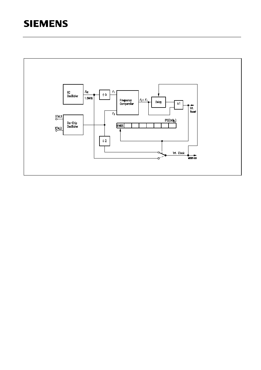
SAB 80C517A/83C517A-5
Semiconductor Group
59
1994-05-01
Figure 12
Functional Block Diagram of the Oscillator Watchdog
SAB 80C517A/83C517A-5
Semiconductor Group
60
1994-05-01
Fast internal reset after power-on
The SAB 80C517A can use the oscillator watchdog unit for a fast internal reset procedure after
power-on.
Normally members of the 8051 family (like the SAB 80C517) enter their default reset state not
before the on-chip oscillator starts. The reason is that the external reset signal must be
internally synchronized and processed in order to bring the device into the correct reset state.
Especially if a crystal is used the start up time of the oscillator is relatively long (typ. 1 ms).
During this time period the pins have an undefined state which could have severe effects e.g.
to actuators connected to port pins.
In the SAB 80C517A the oscillator watchdog unit avoids this situation. However, the oscillator
watchdog must be enabled. In this case, after power-on the oscillator watch-dog's RC
oscillator starts working within a very short start-up time (typ. less than 2 micro-seconds). In
the following the watchdog circuitry detects a failure condition for the on-chip oscillator
because this has not yet started (a failure is always recognized if the watchdog's RC oscillator
runs faster than the on-chip oscillator). As long as this condition is valid the watchdog uses the
RC oscillator output as clock source for the chip rather than the on-chip oscillator's output.This
allows correct resetting of the part and brings also all ports to the defined state.
Delay time between power-on and correct reset state:
Typ.: 18
µ
s
Max.: 34
µ
s
Instruction Set
The SAB 80C517A / 83C517A-5 has the same instruction set as the industry standard 8051
microcontroller.
A pocket guide is available which contains the complete instruction set in functional and
hexadecimal order. Furtheron it provides helpful information about Special Function Registers,
Interrupt Vectors and Assembler Directives.
Literature Information
Title
Ordering No.
Microcontroller Family SAB 8051 Pocket Guide
B158-H6497-X-X-7600
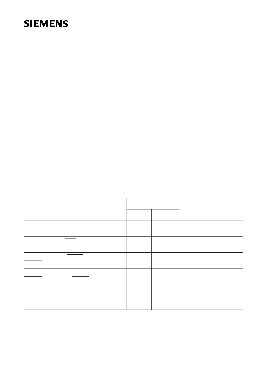
SAB 80C517A/83C517A-5
Semiconductor Group
61
1994-05-01
Absolute Maximum Ratings
Ambient temperature under bias................................................................. ≠ 40 to 110∞ C
Storage temperature ................................................................................... ≠ 65 to 150
o
C
Voltage on
V
CC
pins with respect to ground (
V
SS
) ...................................... ≠ 0.5 V to 6.5 V
Voltage on any pin with respect to ground (
V
SS
) ........................................ ≠ 0.5 to
V
CC
+0.5 V
Input current on any pin during overload condition ..................................... ≠ 10mA to +10mA
Absolute sum of all input currents during overload condition...................... |100mA
|
Power dissipation ........................................................................................ 1 W
Note Stresses above those listed under "Absolute Maximum Ratings" may cause permanent
damage of the device. This is a stress rating only and functional operation of the device
at these or any other conditions above those indicated in the operational sections of this
specification is not implied. Exposure to absolute maximum rating conditions for longer
periods may affect device reliability. During overload conditions (V
IN
>
V
CC
or
V
IN
<
V
SS
)
theVoltage on V
CC
pins with respect to ground (V
SS
) must not exeed the values
definded by the absolute maximum ratings.
DC Characteristics
V
CC
= 5 V + 10 %, ≠ 15 %;
V
SS
= 0 V
T
A
=
0 to 70
o
C for the SAB 80C517A/83C517A-5
T
A
=
≠
40 to 85
o
C for the SAB 80C517A-T3/83C517A-5-T3
T
A
=
≠
40 to 110
o
C for the SAB 80C517A-T4/83C517A-5-T4
Parameter
Symbol
Limit Values
Unit
Test Condition
min.
max.
Input low voltage
(except EA, RESET, HWPD)
V
IL
≠ 0.5
0.2
V
CC
≠
0.1
V
≠
Input low voltage (EA)
V
IL1
≠ 0.5
0.2
V
CC
≠
0.3
V
≠
Input low voltage (HWPD,
RESET)
V
IL2
≠ 0.5
0.2
V
C C
+ 0.1
V
≠
Input high voltage (except
RESET, XTAL2 and HWPD
V
IH
0.2
V
CC
+ 0.9
V
CC
+ 0.5
V
≠
Input high voltage to XTAL2
V
IH1
0.7
V
CC
V
CC
+ 0.5
V
≠
Input high voltage to RESET
and HWPD
V
IH2
0.6
V
CC
V
CC
+ 0.5
V
≠
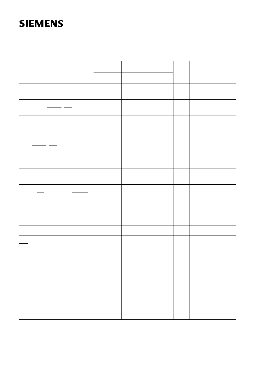
SAB 80C517A/83C517A-5
Semiconductor Group
62
1994-05-01
DC Characteristics (cont'd)
Parameter
Symbol
Limit Values
Unit
Test condition
min.
max.
Output low voltage
(ports 1, 2, 3, 4, 5, 6)
V
OL
≠
0.45
V
I
OL
=1.6
mA
1)
Output low voltage
(ports ALE, PSEN, RO)
V
OL1
≠
0.45
V
I
OL
=3.2 mA
1)
Output high voltage
(ports 1, 2, 3, 4, 5, 6)
V
OH
2.4
0.9
V
CC
≠
≠
V
V
I
OH
=≠80
µ
A
I
OH
=≠10
µ
A
Output high voltage
(port 0 in external bus mode,
ALE, PSEN, RO)
V
OH1
2.4
0.9
V
CC
≠
≠
V
V
I
OH
=≠800
µ
A
2)
I
OH
=≠80
µ
A
2)
Logic input low current
(ports 1, 2, 3, 4, 5, 6)
I
IL
≠ 10
≠ 70
µ
A
V
IN
= 0.45 V
Logical 1-to-0 transition current
(ports 1, 2, 3, 4, 5, 6)
I
TL
≠ 65
≠
650
µ
A
V
IN
= 2 V
Input leakage current
(port 0, EA, ports 7, 8, HWPD)
I
LI
≠
±
100
nA
0.45 <
V
IN
<
V
CC
±
150
nA
0.45 <
V
IN
<
V
CC
T
A
> 100
o
C
Input low current to RESET
for reset
I
IL2
≠ 10
≠100
µ
A
V
IN
= 0.45 V
Input low current (XTAL2)
I
IL3
≠
≠ 15
µ
A
V
IN
= 0.45 V
Input low current
(PE/SWD, OWE)
I
IL4
≠
≠ 20
µ
A
V
IN
= 0.45 V
Pin capacitance
C
IO
≠
10
pF
f
C
= 1 MHz
T
A
= 25
o
C
Power supply current:
Active mode, 12 MHz
7)
Active mode, 18 MHz
7)
Idle mode, 12 MHz
7)
Idle mode, 18 MHz
7)
Slow down mode, 12 MHz
Slow down mode, 18 MHz
Power Down Mode
I
CC
I
CC
I
CC
I
CC
I
CC
I
CC
I
PD
≠
≠
≠
≠
≠
≠
≠
28
37
24
31
12
16
50
mA
mA
mA
mA
mA
mA
µ
A
V
CC
= 5 V,
4)
V
CC
= 5 V,
4)
V
CC
= 5 V,
5)
V
CC
= 5 V,
5)
V
CC
= 5 V,
6)
V
CC
= 5 V,
6)
V
CC
= 2...5.5 V,
3)
Notes see page 61.

SAB 80C517A/83C517A-5
Semiconductor Group
63
1994-05-01
Notes for page 62:
1) Capacitive loading on ports 0 and 2 may cause spurious noise pulses to be superimposed
on the
V
OL
of ALE and ports 1, 3, 4, 5 and 6. The noise is due to external bus capacitance
discharging into the port 0 and port 2 pins when these pins make 1-to-0 transitions during
bus operation. In the worst case (capacitive loading > 100 pF), the noise pulse on ALE line
may exceed 0.8 V. In such cases it may be desirable to qualify ALE with a schmitt-trigger,
or use an address latch with a schmitt-trigger strobe input.
2) Capacitive loading on ports 0 and 2 may cause the
V
OH
on ALE and
PSEN
to momentarily
fall
below the
0.9
V
C C
specification when the address lines are stabilizing.
3)
I
PD
(Power down mode) is measured with:
EA
=
RESET
=
V
CC;
Port0 = Port7 = Port8 =
V
CC
; XTAL1 = N.C.; XTAL2 =
V
SS
;
PE/SWD
= OWE =
V
SS
;
HWDP
=
V
CC
(Software Power Down mode);
V
ARef
=
V
CC
;
V
AGND
=
V
SS
; all other pins are disconnected. Hardware Powerdown
I
PD
: OWE =
V
CC
or
V
SS
. No certain pin connection for the other pins.
4)
I
CC
(active mode) is measured with:
XTAL2 driven with
t
CLCH,
t
CHCL
= 5 ns,
V
IL
=
V
SS
+ 0.5 V,
V
IH
=
V
CC
≠ 0.5 V; XTAL1 = N.C.;
EA = PE
/SWD =
V
CC
; Port0 = Port7 = Port8 =
V
CC
;
HWPD
=
V
CC
;
RESET
=
V
SS
all other pins are disconnected.
I
CC
would be slightly higher if a crystal oscillator is
used (appr. 1 mA).
5)
I
CC
(Idle mode) is measured with all output pins disconnected and with all peripherals
disabled; XTAL2 driven with
t
CLCH
,
t
CHCL
= 5 ns,
V
IL
=
V
SS
+ 0.5 V,
V
IH
=
V
CC
≠ 0.5 V;
XTAL1 = N.C.;
RESET
=
V
CC
;
HWPD
=
V
CC
; Port0 = Port7 = Port8 =
V
CC
;
EA = PE
/SWD =
V
SS
; all other pins are disconnected;
6)
I
CC
(slow down mode) is measured with all output pins disconnected and with all peripher-
als disabled; XTAL2 driven with
t
CLCH,
t
CHCL
= 5 ns,
V
IL
=
V
SS
+ 0.5 V,
V
IH
=
V
CC
≠ 0.5 V;
XTAL1 = N.C.
;RESET
=
V
CC
;
HWPD
=
V
CC
; Port7 = Port8 =
V
CC
;
EA = PE/SWD
=
V
SS
;
all other pins are disconnected;
7)
I
CC
Max
at other frequencies is given by:
active mode:
I
CC
(max) = 1.50*
f
OSC
+ 10
idle mode:
I
CC
(max) = 1.17*
f
OSC
+ 10
where
f
OSC
is the oscillator frequency in MHz.
I
CC
values are given in mA and
measured at
V
CC
= 5 V.

SAB 80C517A/83C517A-5
Semiconductor Group
64
1994-05-01
A/D Converter Characteristics
V
CC
= 5 V + 10 %, ≠ 15 %;
V
SS
= 0 V
V
AREF
=
V
CC
±
5%;
V
AGND
=
V
SS
±
0.2 V;
T
A
=
0 to 70
o
C for the SAB 80C517A/83C517A-5
T
A
=
≠
40 to 85
o
C for the SAB 80C517A-T3/83C517A-5-T3
T
A
=
≠
40 to 110
o
C for the SAB 80C517A-T4/83C517A-5-T4
Parameter
Symbol
Limit values
Unit
Test condition
min.
typ.
max.
Analog input capacitance
C
I
25
70
pF
Sample time
(inc. load time)
T
S
4
t
CY
1)
µ
s
2)
Conversion time
(inc. sample time)
T
C
14
t
CY
1)
µ
s
3)
Total unadjusted error
TUE
±
2
LSB
V
AREF
=
V
CC
V
AGND
=
V
SS
V
AREF
supply current
I
REF
±
20
µ
A
4)
1)
t
CY
= (8*2
ADCL
)
/
f
OSC
; (
t
CY
= 1/
f
ADC
;
f
ADC
=
f
OSC
/(8*2
ADCL
))
2)
This parameter specifies the time during the input capacitance
C
I,
can be charged/discharged by the
external source. It must be guaranteed, that the input capacitance
C
I,
, is fully loaded within this time.
4TCY is 2
µ
s at the
f
OSC
= 16 MHz. After the end of the sample time
T
S
, changes of the analog input
voltage have no effect on the conversion result.
3)
This parameter includes the sample time
T
S.
14TCY is 7
µ
s at
f
OSC
= 16 MHz.
4)
The differencial impedance
r
D
of the analog reference source must be less than 1 K
at reference supply
voltage.
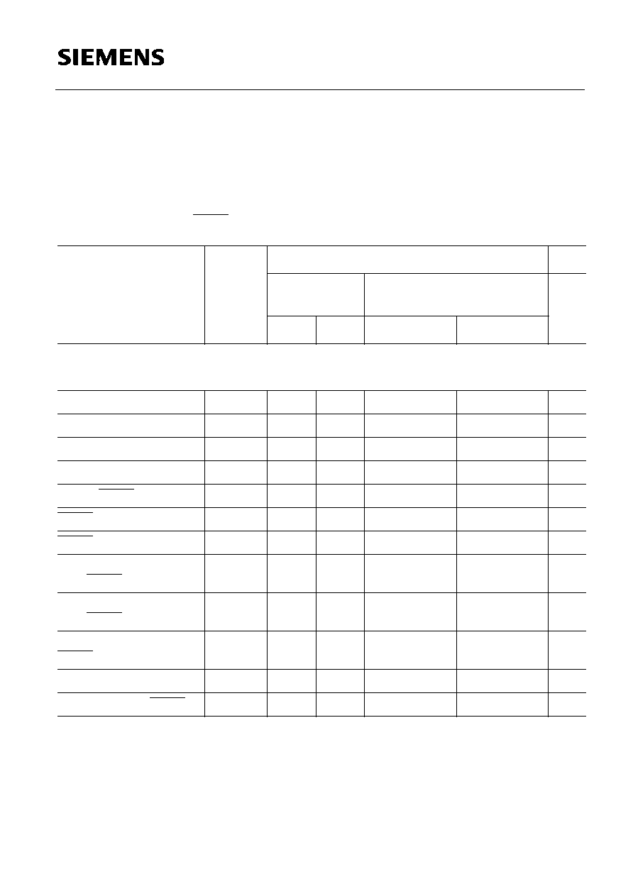
SAB 80C517A/83C517A-5
Semiconductor Group
65
1994-05-01
AC Characteristics
V
CC
= 5 V + 10 %, ≠ 15 %;
V
SS
= 0 V
T
A
=
0 to 70
o
C for the SAB 80C517A/83C517A-5
T
A
=
≠
40 to 85
o
C for the SAB 80C517A-T3/83C517A-5-T3
T
A
=
≠
40 to110
o
C for the SAB 80C517A-T4/83C517A-5-T4
(
C
L
for port 0, ALE and
PSEN outputs = 100 pF;
C
L
for all other outputs = 80 pF)
Parameter
Symbol
Limit Values
Unit
18 MHz Clock
Variable Clock
1/
t
CLCL
= 3.5 MHz to 18 MHz
min.
max.
min.
max.
Program Memory Characteristics
ALE pulse width
t
LHLL
71
≠
2
t
CLCL
≠ 40
≠
ns
Address setup to ALE
t
AVLL
26
≠
t
CLCL
≠ 30
≠
ns
Address hold after ALE
t
LLAX
26
≠
t
CLCL
≠ 30
≠
ns
ALE to valid instruction
t
LLIV
≠
122
≠
4
t
CLCL
≠ 100
ns
ALE to
PSEN
t
LLPL
31
≠
t
CLCL
≠ 25
≠
ns
PSEN pulse width
t
PLPH
132
≠
3
t
CLCL
≠ 35
≠
ns
PSEN to valid instruction
t
PLIV
≠
92
≠
3
t
CLCL
≠ 75
ns
Input instruction hold
after PSEN
t
PXIX
0
≠
0
ns
Input instruction float
after PSEN
t
PXIZ
≠
46
≠
t
CLCL
≠ 10
ns
Address valid after
PSEN
t
PXAV*)
48
≠
t
CLCL
≠ 8
≠
ns
Address to valid instr in
t
AVIV
≠
218
≠
5
t
CLCL
≠ 60
ns
Address float to PSEN
t
AZPL
0
≠
0
≠
ns
*)
Interfacing the SAB 80C517A to devices with float times up to 45 ns is permissible.
This limited bus contention will not cause any damage to port 0 drivers.

SAB 80C517A/83C517A-5
Semiconductor Group
66
1994-05-01
AC Characteristics (cont'd)
Parameter
Symbol
Limit Values
Unit
18 MHz Clock
Variable Clock
1/
t
CLCL
= 3.5 MHz to 18 MHz
min.
max.
min.
max.
External Data Memory Characteristics
RD pulse width
t
RLRH
233
≠
6
t
CLCL
≠ 100
≠
ns
WR pulse width
t
WLWH
233
≠
6
t
CLCL
≠ 100
≠
ns
Address hold after ALE
t
LLAX2
81
≠
2
t
CLCL
≠ 30
≠
ns
RD to valid data in
t
RLDV
≠
128
≠
5
t
CLCL
≠ 150
ns
Data hold after RD
t
RHDX
0
≠
0
≠
ns
Data float after RD
t
RHDZ
≠
51
≠
2
t
CLCL
≠ 60
ns
ALE to valid data in
t
LLDV
≠
294
≠
8
t
CLCL
≠ 150
ns
Address to valid data in
t
AVDV
≠
335
≠
9
t
CLCL
≠ 165
ns
ALE to WR or RD
t
LLWL
117
217
3
t
CLCL
≠ 50
3
t
CLCL
+50
ns
WR or RD high to ALE
high
t
WHLH
16
96
t
CLCL
≠ 40
t
CLCL
+40
ns
Address valid to WR
t
AVWL
92
≠
4
t
CLCL
≠ 130
≠
ns
Data valid to WR
transition
t
QVWX
11
≠
t
CLCL
≠ 45
≠
ns
Data setup before WR
t
QVWH
239
≠
7
t
CLCL
≠ 150
≠
ns
Data hold after WR
t
WHQX
16
≠
t
CLCL
≠ 40
≠
ns
Address float after RD
t
RLAZ
≠
0
≠
0
ns
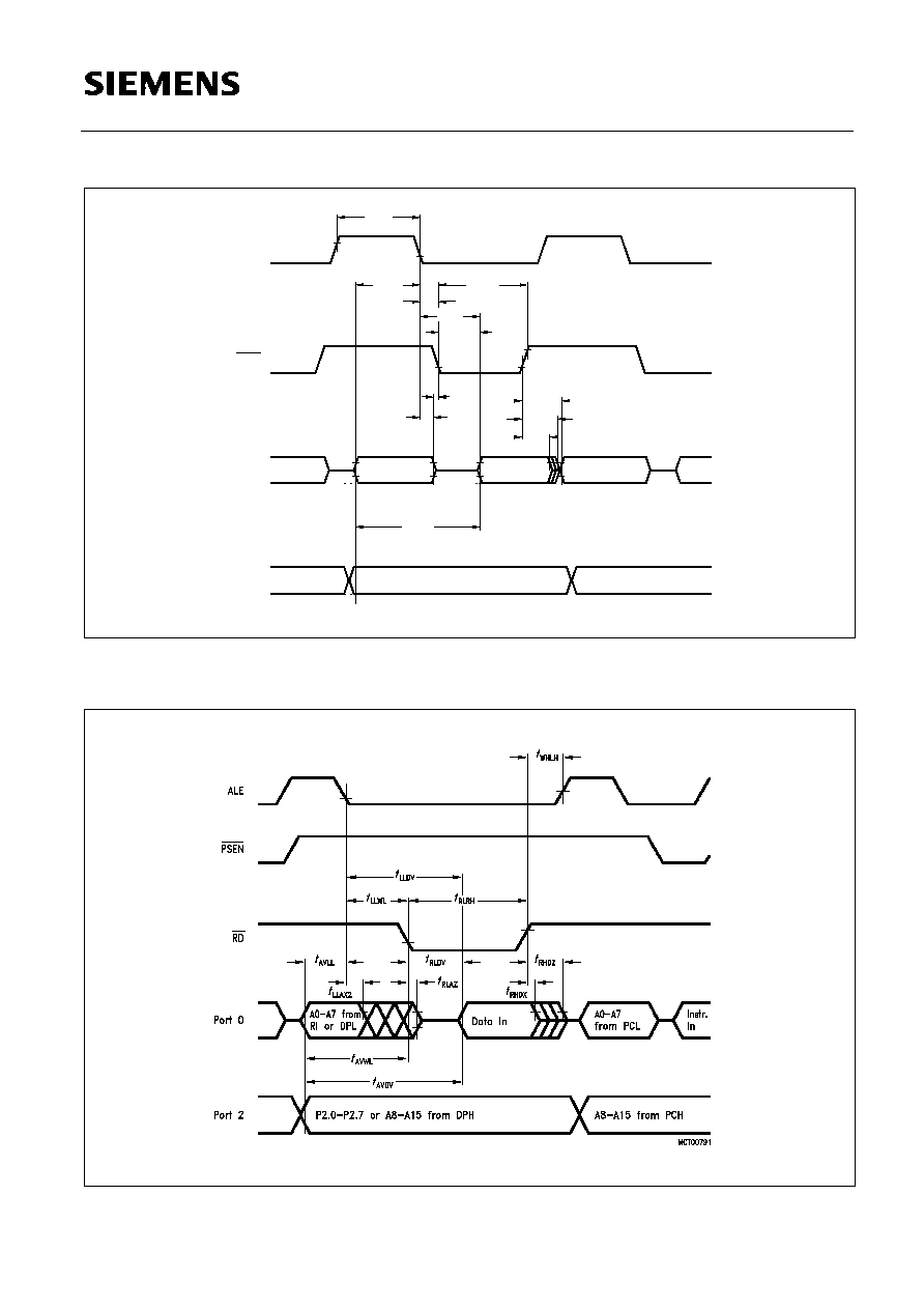
SAB 80C517A/83C517A-5
Semiconductor Group
67
1994-05-01
Program Memory Read Cycle
Data Memory Read Cycle
MCT00096
ALE
PSEN
Port 2
LHLL
t
A8 - A15
A8 - A15
A0 - A7
Instr.IN
A0 - A7
Port 0
t
AVLL
PLPH
t
t
LLPL
t
LLIV
t
PLIV
t
AZPL
t
LLAX
t
PXIZ
t
PXIX
t
AVIV
t
PXAV

SAB 80C517A/83C517A-5
Semiconductor Group
68
1994-05-01
Data Memory Write Cycle
MCT00098
ALE
PSEN
Port 2
WHLH
t
Port 0
WR
t
WLWH
t
LLWL
t
QVWX
t
AVLL
t
LLAX2
t
QVWH
t
AVWL
t
WHQX
A0 - A7 from
Ri or DPL
from PCL
A0 - A7
Instr.IN
Data OUT
A8 - A15 from PCH
P2.0 - P2.7 or A8 - A15 from DPH
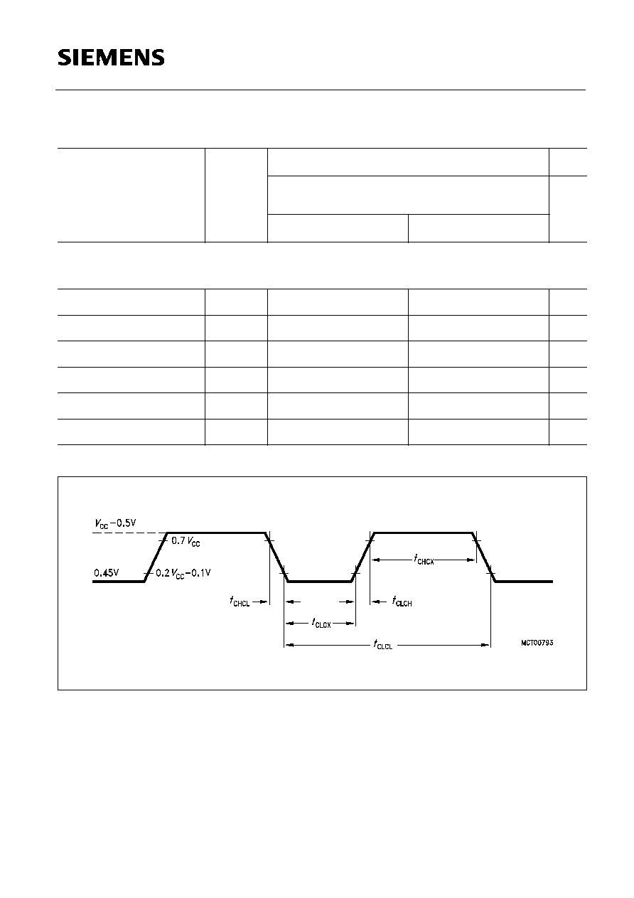
SAB 80C517A/83C517A-5
Semiconductor Group
69
1994-05-01
AC Characteristics (cont'd)
External Clock Cycle
Parameter
Symbol
Limit Values
Unit
Variable clock
Frequ. = 3.5 MHz to 18 MHz
min.
max.
External Clock Drive
Oscillator period
t
CLCL
55.6
285
ns
High time
t
CHCX
20
t
CLCL-
t
CHCX
ns
Low time
t
CLCX
20
t
CLCL-
t
CHCX
ns
Rise time
t
CLCH
≠
20
ns
Fall time
t
CHCL
≠
20
ns
Oscillator frequency
1/
t
CLC
3.5
18
MHz
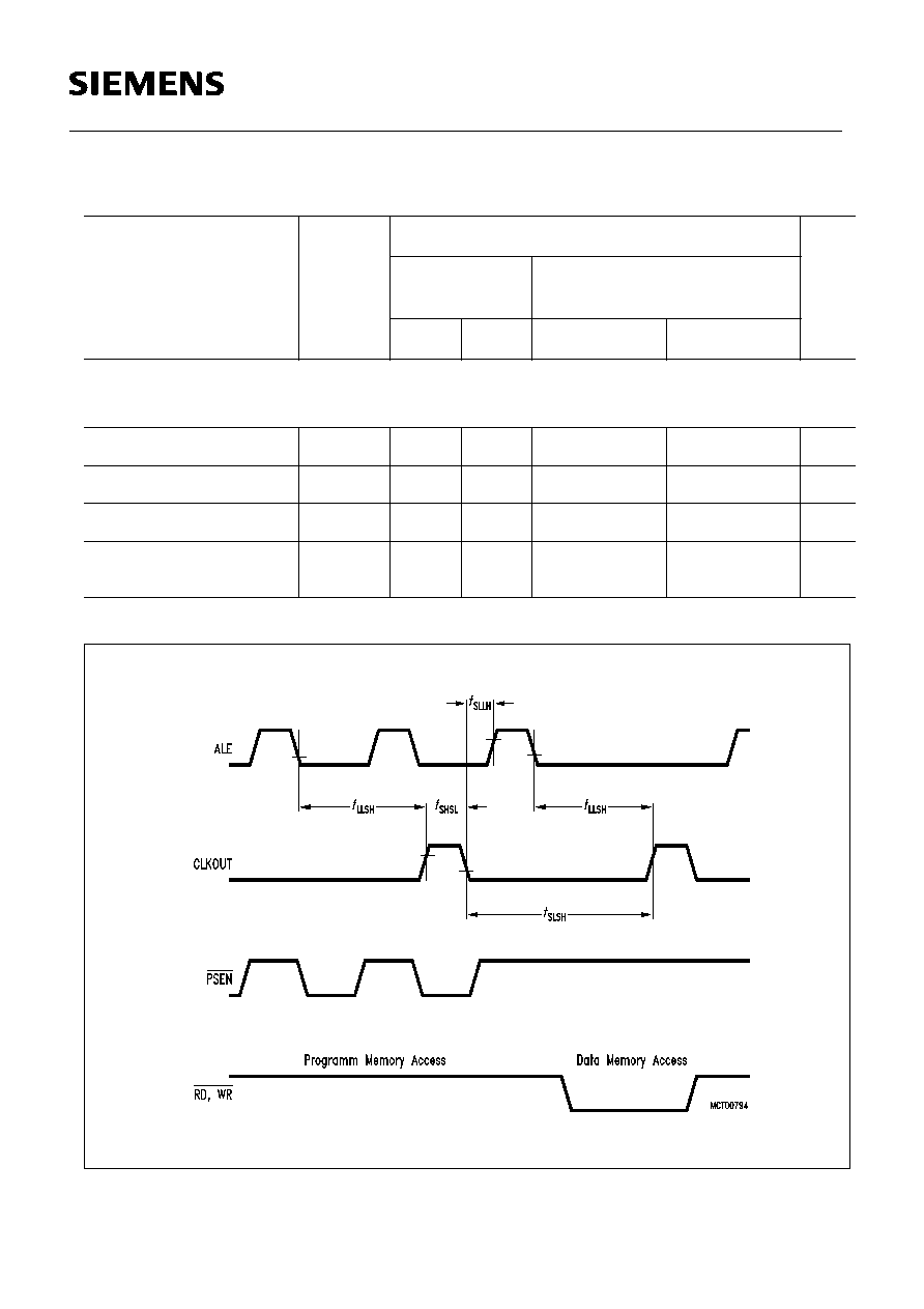
SAB 80C517A/83C517A-5
Semiconductor Group
70
1994-05-01
AC Characteristics (cont'd)
System Clock Timing
Parameter
Symbol
Limit Values
Unit
18 MHz clock
Variable Clock
1/
t
CLCL
= 3.5 MHz to 18 MHz
min.
max.
min.
max.
System Clock Timing
ALE to CLKOUT
t
LLSH
349
≠
7
t
CLCL
≠ 40
≠
ns
CLKOUT high time
t
SHSL
71
≠
2
t
CLCL
≠ 40
≠
ns
CLKOUT low time
t
SLSH
516
≠
10
t
CLCL
≠ 40
≠
ns
CLKOUT low to ALE
high
t
SLLH
16
96
t
CLCL
≠ 40
t
CLCL
+40
ns
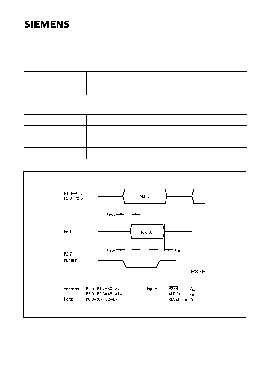
SAB 80C517A/83C517A-5
Semiconductor Group
71
1994-05-01
ROM Verification Characteristics
T
A
= 25∞C
±
5∞C;
V
CC
= 5 V
±
10%;
V
SS
= 0 V
ROM Verification Mode 1
Parameter
Symbol
Limit Values
Unit
min.
max.
ROM Verification Mode 1 (Standard Verify Mode for not Read Protected ROM)
Address to valid data
t
AVQV
≠
48
t
CLCL
ns
ENABLE to valid data
t
ELQV
≠
48
t
CLCL
ns
Data float after ENABLE
t
EHOZ
0
48
t
CLCL
ns
Oscillator frequency
1/
t
CLCL
4
6
MHz
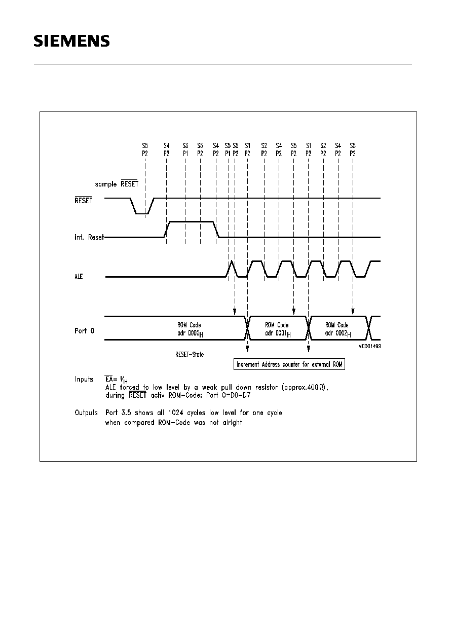
SAB 80C517A/83C517A-5
Semiconductor Group
72
1994-05-01
ROM Verification Mode 2 (New Verify Mode for Protected and not Protected ROM)
ROM Verification Mode 2
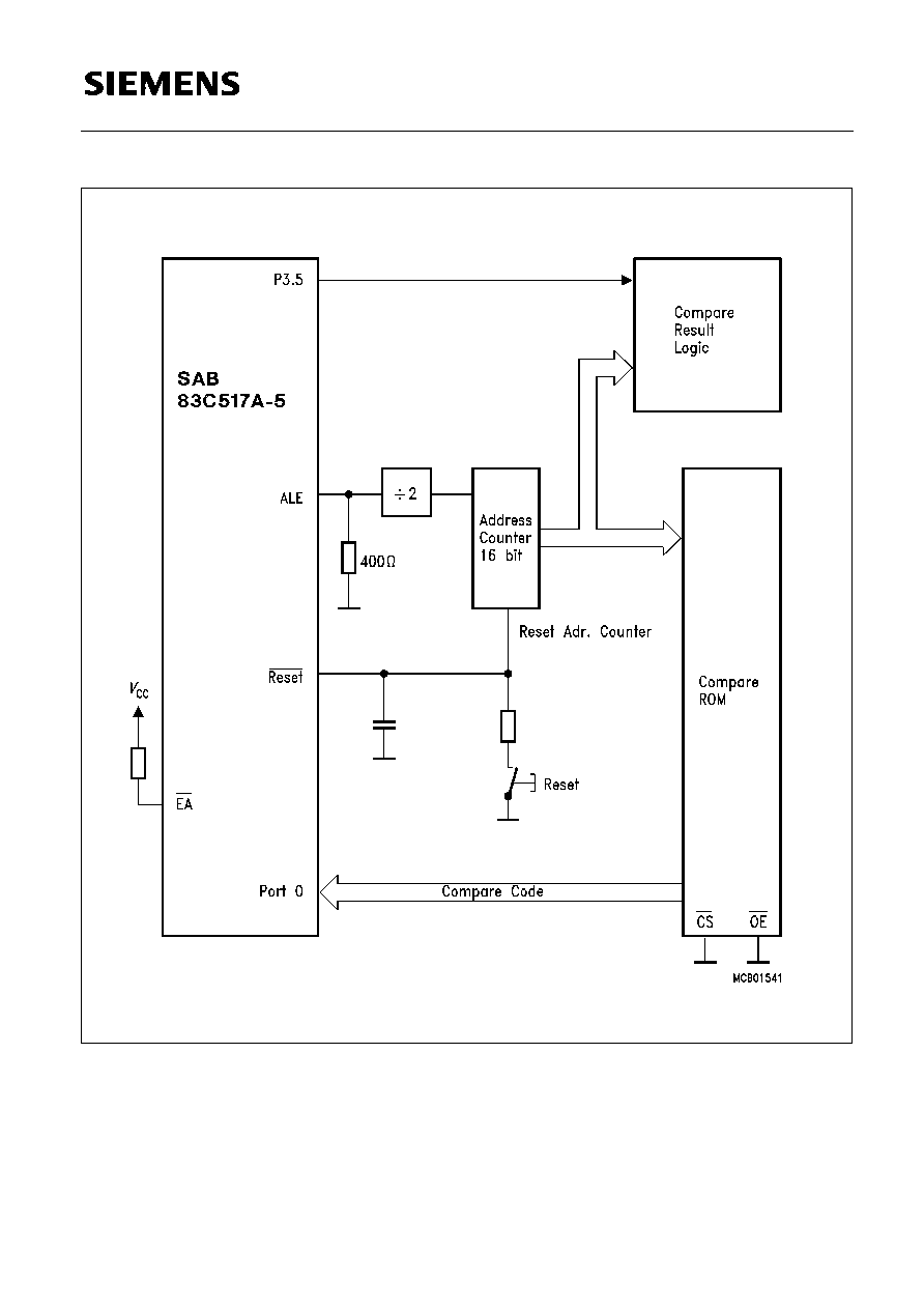
SAB 80C517A/83C517A-5
Semiconductor Group
73
1994-05-01
Application Circuitry for Verifying the Internal ROM
SAB 80C517A/83C517A-5
Semiconductor Group
74
1994-05-01
AC Testing: Input, Output Waveforms
AC Testing: Float Waveforms
Recommended Oscillator Circuits
AC Inputs during testing are driven at
V
CC
- 0.5 V for a logic '1' and 0.45 V for a logic '0'. Timing measure-
ments are made at
V
IHmin
for a logic '1' and
V
ILmax
for a logic '0'.
For timing purposes a port pin is no longer floating when a 100 mV change from load voltage occurs and
begins to float when a 100 mV change from the loaded
V
OH
/
V
OL
level occurs.
I
OL
/
I
OH
±
20 mA.

SAB 80C517A/83C517A-5
Semiconductor Group
75
1994-05-01
Figure 1
P-MQFP-100-2 Package Outlines
GPM05623
Plastic Package, P-MQFP-100-2 (SMD)
(Plastic Metric Quad Flat Package)
Sorts of Packing
Package outlines for tubes, trays etc. are contained in our
Data Book "Package Information"
SMD = Surface Mounted Device
Dimensions in mm

SAB 80C517A/83C517A-5
Semiconductor Group
76
1994-05-01
Figure 2
P-LCC-84-2 Package Outlines
GPM05623
Plastic Package, P-LCC-84-2 (SMD)
(Plastic Leaded Chip Carrier)
Sorts of Packing
Package outlines for tubes, trays etc. are contained in our
Data Book "Package Information"
SMD = Surface Mounted Device
Dimensions in mm