
Data Sheet 12.96 (Advance Information)
Microcomputer Components
C167CR-16RM
16-Bit CMOS Single-Chip Microcontrollers

Controller Area Network (CAN): License of Robert Bosch GmbH
C167CR-16RM
Revision History:
Original Version 12.96 (Advance Information)
Previous Releases:
-
Page
Subjects (compared to Data Sheet C167CR, 06.95)
21
Incremental Interface Mode added.
22
T3 capture trigger for CAPREL added.
Edition 12.96
Published by Siemens AG, Bereich Halbleiter, Marketing-Kommunikation
Balanstraþe 73, D-81541 M¸nchen.
© Siemens AG 1996. All Rights Reserved.
As far as patents or other rights of third parties are concerned, liability is only assumed for
components per se, not for applications, processes and circuits implemented within components or
assemblies.
The information describes the type of component and shall not be considered as assured
characteristics.
Terms of delivery and rights to change design reserved.
For questions on technology, delivery and prices please contact the Offices of Siemens
Aktiengesellschaft in Germany or the Siemens Companies and Representatives worldwide.
Due to technical requirements components may contain dangerous substances. For information on
the type in question please contact your nearest Siemens Office, Components Group.
Siemens AG is an approved CECC manufacturer.

q
High Performance 16-bit CPU with 4-Stage Pipeline
q
100 ns Instruction Cycle Time at 20 MHz CPU Clock
q
500 ns Multiplication (16
◊
16 bit), 1
µ
s Division (32 / 16 bit)
q
Enhanced Boolean Bit Manipulation Facilities
q
Additional Instructions to Support HLL and Operating Systems
q
Register-Based Design with Multiple Variable Register Banks
q
Single-Cycle Context Switching Support
q
Clock Generation via on-chip PLL or via direct clock input
q
Up to 16 MBytes Linear Address Space for Code and Data
q
2 KBytes On-Chip Internal RAM (IRAM)
q
2 KBytes On-Chip Extension RAM (XRAM)
q
128 KBytes On-Chip ROM
q
Programmable External Bus Characteristics for Different Address Ranges
q
8-Bit or 16-Bit External Data Bus
q
Multiplexed or Demultiplexed External Address/Data Buses
q
Five Programmable Chip-Select Signals
q
Hold- and Hold-Acknowledge Bus Arbitration Support
q
1024 Bytes On-Chip Special Function Register Area
q
Idle and Power Down Modes
q
8-Channel Interrupt-Driven Single-Cycle Data Transfer Facilities via Peripheral Event
Controller (PEC)
q
16-Priority-Level Interrupt System with 56 Sources, Sample-Rate down to 50 ns
q
16-Channel 10-bit A/D Converter with 9.7
µ
s Conversion Time
q
Two 16-Channel Capture/Compare Units
q
4-Channel PWM Unit
q
Two Multi-Functional General Purpose Timer Units with 5 Timers
q
Two Serial Channels (Synchronous/Asynchronous and High-Speed-Synchronous)
q
On-Chip CAN Interface with 15 Message Objects (Full-CAN/Basic-CAN)
q
Programmable Watchdog Timer
q
Up to 111 General Purpose I/O Lines, partly with Selectable Input Thresholds and Hysteresis
q
Supported by a Wealth of Development Tools like C-Compilers, Macro-Assembler Packages,
Emulators, Evaluation Boards, HLL-Debuggers, Simulators, Logic Analyzer Disassemblers,
Programming Boards
q
On-Chip Bootstrap Loader
q
144-Pin MQFP Package (EIAJ)
This document describes the SAB-C167CR-16RM and the SAK-C167CR-16RM. For simplicity all
versions are referred to by the term C167CR-16RM throughout this document.
C16x-Family of
High-Performance CMOS 16-Bit Microcontrollers
Advance Information
C167CR-16RM 16-Bit Microcontroller
C167CR-16RM
1
12.96
20Dec96@09:25h Intermediate Version
Semiconductor Group
2
C167CR-16RM
Introduction
The C167CR-16RM is a new derivative of the Siemens C16x Family of full featured single-chip
CMOS microcontrollers. It combines high CPU performance (up to 10 million instructions per
second) with high peripheral functionality and enhanced IO-capabilities. It also provides on-chip
ROM, on-chip high-speed RAM and clock generation via PLL.
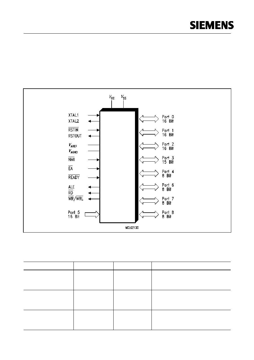
Figure 1
Logic Symbol
Ordering Information
Type
Ordering Code
Package
Function
SAB-C167CR-16RM
Q67121-D...
P-MQFP-144-1
16-bit microcontroller with
2 * 2 KByte RAM
Temperature range 0 to +70 ∞C
SAF-C167CR-16RM
Q67121-D...
P-MQFP-144-1
16-bit microcontroller with
2 * 2 KByte RAM
Temperature range -40 to +85 ∞C
SAK-C167CR-16RM
Q67121-D...
P-MQFP-144-1
16-bit microcontroller with
2 * 2 KByte RAM
Temperature range -40 to +125 ∞C
C167CR-
16RM
20Dec96@09:25h Intermediate Version
3
Semiconductor Group
C167CR-16RM
Note: The ordering codes (Q67121-D...) for the Mask-ROM versions are defined for each product
after verifiction of the respective ROM code.
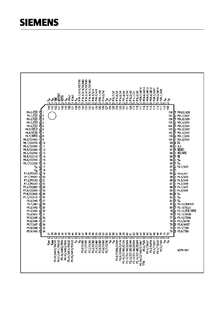
Pin Configuration
(top view)
Figure 2
C167CR-16RM
A22/CAN_TxD
/CAN_RxD
20Dec96@09:25h Intermediate Version
Semiconductor Group
4
C167CR-16RM
Pin Definitions and Functions
Symbol
Pin
Number
Input (I)
Output (O)
Function
P6.0 ≠
P6.7
1 -
8
1
...
5
6
7
8
I/O
O
...
O
I
O
O
Port 6 is an 8-bit bidirectional I/O port. It is bit-wise
programmable for input or output via direction bits. For a pin
configured as input, the output driver is put into high-
impedance state. Port 6 outputs can be configured as push/
pull or open drain drivers.
The following Port 6 pins also serve for alternate functions:
P6.0
CS0
Chip Select 0 Output
...
...
...
P6.4
CS4
Chip Select 4 Output
P6.5
HOLD
External Master Hold Request Input
P6.6
HLDA
Hold Acknowledge Output
P6.7
BREQ
Bus Request Output
P8.0 ≠
P8.7
9 -
16
9
...
16
I/O
I/O
...
I/O
Port 8 is an 8-bit bidirectional I/O port. It is bit-wise
programmable for input or output via direction bits. For a pin
configured as input, the output driver is put into high-
impedance state. Port 8 outputs can be configured as push/
pull or open drain drivers. The input threshold of Port 8 is
selectable (TTL or special).
The following Port 8 pins also serve for alternate functions:
P8.0
CC16IO
CAPCOM2: CC16 Cap.-In/Comp.Out
...
...
...
P8.7
CC23IO
CAPCOM2: CC23 Cap.-In/Comp.Out
P7.0 ≠
P7.7
19 -
26
19
...
22
23
...
26
I/O
O
...
O
I/O
...
I/O
Port 7 is an 8-bit bidirectional I/O port. It is bit-wise
programmable for input or output via direction bits. For a pin
configured as input, the output driver is put into high-
impedance state. Port 7 outputs can be configured as push/
pull or open drain drivers. The input threshold of Port 7 is
selectable (TTL or special).
The following Port 7 pins also serve for alternate functions:
P7.0
POUT0
PWM Channel 0 Output
...
...
...
P7.3
POUT3
PWM Channel 3 Output
P7.4
CC28IO
CAPCOM2: CC28 Cap.-In/Comp.Out
...
...
...
P7.7
CC31IO
CAPCOM2: CC31 Cap.-In/Comp.Out

20Dec96@09:25h Intermediate Version
5
Semiconductor Group
C167CR-16RM
P5.0 ≠
P5.15
27 ≠ 36
39 ≠ 44
39
40
41
42
43
44
I
I
I
I
I
I
I
I
Port 5 is a 16-bit input-only port with Schmitt-Trigger
characteristics. The pins of Port 5 also serve as the (up to 16)
analog input channels for the A/D converter, where P5.x
equals ANx (Analog input channel x), or they serve as timer
inputs:
P5.10
T6EUD
GPT2 Timer T6 Ext.Up/Down Ctrl.Input
P5.11
T5EUD
GPT2 Timer T5 Ext.Up/Down Ctrl.Input
P5.12
T6IN
GPT2 Timer T6 Count Input
P5.13
T5IN
GPT2 Timer T5 Count Input
P5.14
T4EUD
GPT1 Timer T4 Ext.Up/Down Ctrl.Input
P5.15
T2EUD
GPT1 Timer T2 Ext.Up/Down Ctrl.Input
P2.0 ≠
P2.15
47 ≠ 54
57 - 64
47
...
54
57
...
64
I/O
I/O
...
I/O
I/O
I
...
I/O
I
I
Port 2 is a 16-bit bidirectional I/O port. It is bit-wise
programmable for input or output via direction bits. For a pin
configured as input, the output driver is put into high-
impedance state. Port 2 outputs can be configured as push/
pull or open drain drivers. The input threshold of Port 2 is
selectable (TTL or special).
The following Port 2 pins also serve for alternate functions:
P2.0
CC0IO
CAPCOM: CC0 Cap.-In/Comp.Out
...
...
...
P2.7
CC7IO
CAPCOM: CC7 Cap.-In/Comp.Out
P2.8
CC8IO
CAPCOM: CC8 Cap.-In/Comp.Out,
EX0IN
Fast External Interrupt 0 Input
...
...
...
P2.15
CC15IO
CAPCOM: CC15 Cap.-In/Comp.Out,
EX7IN
Fast External Interrupt 7 Input
T7IN
CAPCOM2 Timer T7 Count Input
Pin Definitions and Functions (cont'd)
Symbol
Pin
Number
Input (I)
Output (O)
Function
20Dec96@09:25h Intermediate Version
Semiconductor Group
6
C167CR-16RM
P3.0 ≠
P3.13,
P3.15
65 ≠ 70,
73 ≠ 80,
81
65
66
67
68
69
70
73
74
75
76
77
78
79
80
81
I/O
I/O
I/O
I
O
I
O
I
I
I
I
I/O
I/O
O
I/O
O
O
I/O
O
Port 3 is a 15-bit (P3.14 is missing) bidirectional I/O port. It is
bit-wise programmable for input or output via direction bits.
For a pin configured as input, the output driver is put into high-
impedance state. Port 3 outputs can be configured as push/
pull or open drain drivers. The input threshold of Port 3 is
selectable (TTL or special).
The following Port 3 pins also serve for alternate functions:
P3.0
T0IN
CAPCOM Timer T0 Count Input
P3.1
T6OUT
GPT2 Timer T6 Toggle Latch Output
P3.2
CAPIN
GPT2 Register CAPREL Capture Input
P3.3
T3OUT
GPT1 Timer T3 Toggle Latch Output
P3.4
T3EUD
GPT1 Timer T3 Ext.Up/Down Ctrl.Input
P3.5
T4IN
GPT1 Timer T4 Input for
Count/Gate/Reload/Capture
P3.6
T3IN
GPT1 Timer T3 Count/Gate Input
P3.7
T2IN
GPT1 Timer T2 Input for
Count/Gate/Reload/Capture
P3.8
MRST
SSC Master-Rec./Slave-Transmit I/O
P3.9
MTSR
SSC Master-Transmit/Slave-Rec. O/I
P3.10
T
◊
D0
ASC0 Clock/Data Output (Asyn./Syn.)
P3.11
R
◊
D0
ASC0 Data Input (Asyn.) or I/O (Syn.)
P3.12
BHE
Ext. Memory High Byte Enable Signal,
WRH
Ext. Memory High Byte Write Strobe
P3.13
SCLK
SSC Master Clock Outp./Slave Cl. Inp.
P3.15
CLKOUT
System Clock Output (=CPU Clock)
P4.0 ≠
P4.7
85 - 92
85
...
89
90
91
92
I/O
O
...
O
O
I
O
O
O
Port 4 is an 8-bit bidirectional I/O port. It is bit-wise
programmable for input or output via direction bits. For a pin
configured as input, the output driver is put into high-
impedance state.
In case of an external bus configuration, Port 4 can be used to
output the segment address lines:
P4.0
A16
Least Significant Segment Addr. Line
...
...
...
P4.4
A20
Segment Address Line
P4.5
A21
Segment Address Line,
CAN_RxD CAN Receive Data Input
P4.6
A22
Segment Address Line,
CAN_TxD CAN Transmit Data Output
P4.7
A23
Most Significant Segment Addr. Line
RD
95
O
External Memory Read Strobe. RD is activated for every
external instruction or data read access.
Pin Definitions and Functions (cont'd)
Symbol
Pin
Number
Input (I)
Output (O)
Function

20Dec96@09:25h Intermediate Version
7
Semiconductor Group
C167CR-16RM
WR/
WRL
96
O
External Memory Write Strobe. In WR-mode this pin is
activated for every external data write access. In WRL-mode
this pin is activated for low byte data write accesses on a 16-
bit bus, and for every data write access on an 8-bit bus. See
WRCFG in register SYSCON for mode selection.
READY
97
I
Ready Input. When the Ready function is enabled, a high
level at this pin during an external memory access will force
the insertion of memory cycle time waitstates until the pin
returns to a low level.
ALE
98
O
Address Latch Enable Output. Can be used for latching the
address into external memory or an address latch in the
multiplexed bus modes.
EA
99
I
External Access Enable pin. A low level at this pin during and
after Reset forces the C167CR-16RM to begin instruction
execution out of external memory. A high level forces
execution out of the internal ROM. ROMless versions must
have this pin tied to `0'.
PORT0:
P0L.0 ≠
P0L.7,
P0H.0 -
P0H.7
100 ≠
107
108,
111-117
I/O
PORT0 consists of the two 8-bit bidirectional I/O ports P0L
and P0H. It is bit-wise programmable for input or output via
direction bits. For a pin configured as input, the output driver
is put into high-impedance state.
In case of an external bus configuration, PORT0 serves as
the address (A) and address/data (AD) bus in multiplexed bus
modes and as the data (D) bus in demultiplexed bus modes.
Demultiplexed bus modes:
Data Path Width:
8-bit
16-bit
P0L.0 ≠ P0L.7:
D0 ≠ D7
D0 - D7
P0H.0 ≠ P0H.7:
I/O
D8 - D15
Multiplexed bus modes:
Data Path Width:
8-bit
16-bit
P0L.0 ≠ P0L.7:
AD0 ≠ AD7
AD0 - AD7
P0H.0 ≠ P0H.7:
A8 - A15
AD8 - AD15
Pin Definitions and Functions (cont'd)
Symbol
Pin
Number
Input (I)
Output (O)
Function
20Dec96@09:25h Intermediate Version
Semiconductor Group
8
C167CR-16RM
PORT1:
P1L.0 ≠
P1L.7,
P1H.0 -
P1H.7
118 ≠
125
128 ≠
135
132
133
134
135
I/O
I
I
I
I
PORT1 consists of the two 8-bit bidirectional I/O ports P1L
and P1H. It is bit-wise programmable for input or output via
direction bits. For a pin configured as input, the output driver
is put into high-impedance state. PORT1 is used as the 16-bit
address bus (A) in demultiplexed bus modes and also after
switching from a demultiplexed bus mode to a multiplexed bus
mode.
The following PORT1 pins also serve for alternate functions:
P1H.4
CC24IO
CAPCOM2: CC24 Capture Input
P1H.5
CC25IO
CAPCOM2: CC25 Capture Input
P1H.6
CC26IO
CAPCOM2: CC26 Capture Input
P1H.7
CC27IO
CAPCOM2: CC27 Capture Input
XTAL1
XTAL2
138
137
I
O
XTAL1:
Input to the oscillator amplifier and input to the
internal clock generator
XTAL2:
Output of the oscillator amplifier circuit.
To clock the device from an external source, drive XTAL1,
while leaving XTAL2 unconnected. Minimum and maximum
high/low and rise/fall times specified in the AC Characteristics
must be observed.
RSTIN
140
I
Reset Input with Schmitt-Trigger characteristics. A low level at
this pin for a specified duration while the oscillator is running
resets the C167CR-16RM. An internal pullup resistor permits
power-on reset using only a capacitor connected to
V
SS
.
RSTOUT 141
O
Internal Reset Indication Output. This pin is set to a low level
when the part is executing either a hardware-, a software- or a
watchdog timer reset. RSTOUT remains low until the EINIT
(end of initialization) instruction is executed.
NMI
142
I
Non-Maskable Interrupt Input. A high to low transition at this
pin causes the CPU to vector to the NMI trap routine. When
the PWRDN (power down) instruction is executed, the NMI
pin must be low in order to force the C167CR-16RM to go into
power down mode. If NMI is high, when PWRDN is executed,
the part will continue to run in normal mode.
If not used, pin NMI should be pulled high externally.
V
AREF
37
-
Reference voltage for the A/D converter.
V
AGND
38
-
Reference ground for the A/D converter.
V
PP
84
-
Flash programming voltage. This pin accepts the
programming voltage for flash versions of the C167CR-16RM.
Note: This pin is not connected (NC) on non-flash versions.
Pin Definitions and Functions (cont'd)
Symbol
Pin
Number
Input (I)
Output (O)
Function

20Dec96@09:25h Intermediate Version
9
Semiconductor Group
C167CR-16RM
V
CC
17, 46,
56, 72,
82, 93,
109,
126,
136, 144
-
Digital Supply Voltage:
+ 5 V during normal operation and idle mode.
2.5 V during power down mode.
V
SS
18, 45,
55, 71,
83, 94,
110,
127,
139, 143
-
Digital Ground.
Pin Definitions and Functions (cont'd)
Symbol
Pin
Number
Input (I)
Output (O)
Function
20Dec96@09:25h Intermediate Version
Semiconductor Group
10
C167CR-16RM
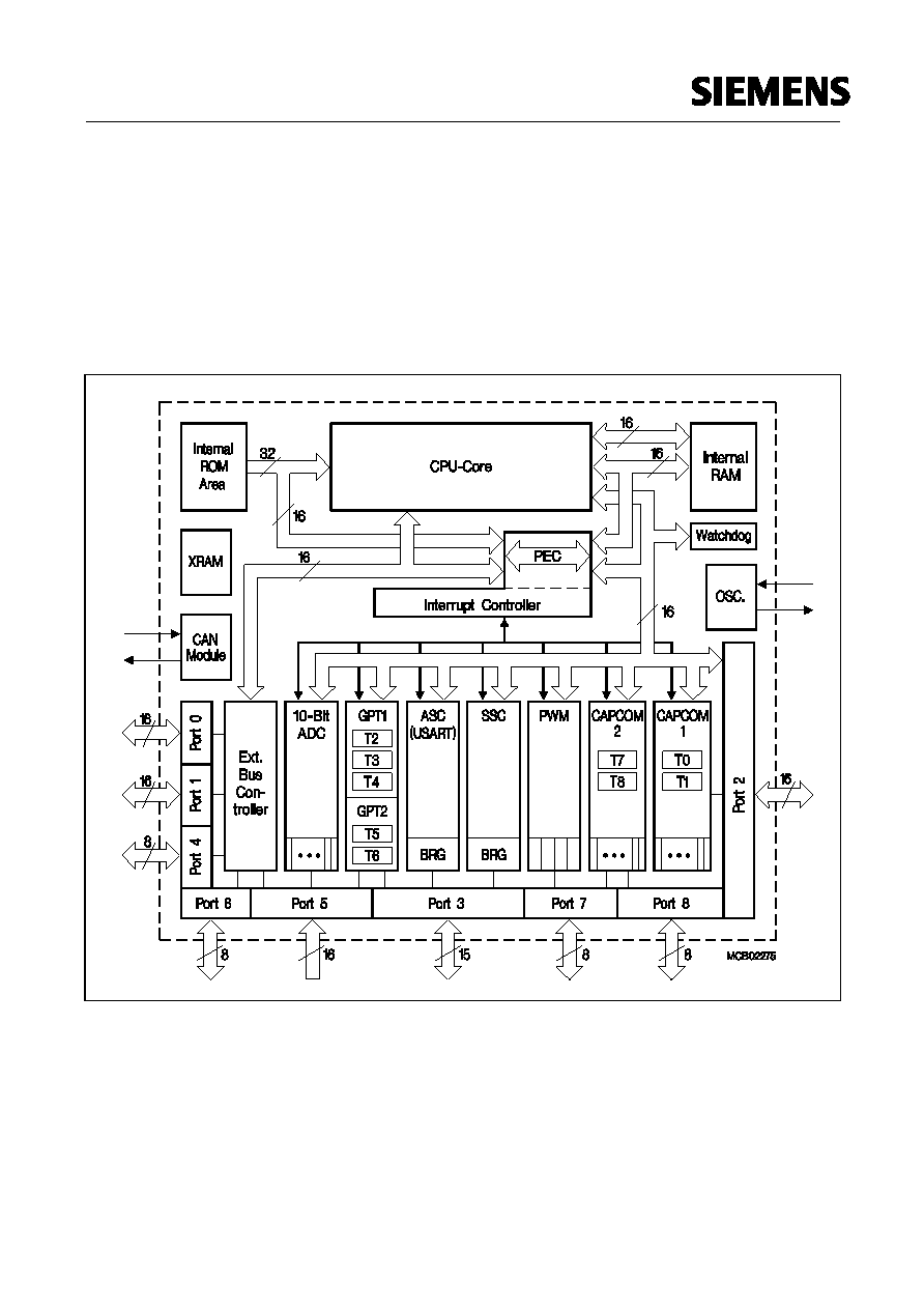
Functional Description
The architecture of the C167CR-16RM combines advantages of both RISC and CISC processors
and of advanced peripheral subsystems in a very well-balanced way. The following block diagram
gives an overview of the different on-chip components and of the advanced, high bandwidth internal
bus structure of the C167CR-16RM.
Note: All time specifications refer to a CPU clock of 20 MHz
(see definition in the AC Characteristics section).
Figure 3
Block Diagram

20Dec96@09:25h Intermediate Version
11
Semiconductor Group
C167CR-16RM
Memory Organization
The memory space of the C167CR-16RM is configured in a Von Neumann architecture which
means that code memory, data memory, registers and I/O ports are organized within the same
linear address space which includes 16 MBytes. The entire memory space can be accessed
bytewise or wordwise. Particular portions of the on-chip memory have additionally been made
directly bitaddressable.
The C167CR-16RM contains 128 KBytes of on-chip mask-programmable ROM for code or
constant data. The lower 32 KBytes of the on-chip ROM can be mapped either to segment 0 or
segment 1.
2 KBytes of on-chip Internal RAM are provided as a storage for user defined variables, for the
system stack, general purpose register banks and even for code. A register bank can consist of up
to 16 wordwide (R0 to R15) and/or bytewide (RL0, RH0, ..., RL7, RH7) so-called General Purpose
Registers (GPRs).
1024 bytes (2 * 512 bytes) of the address space are reserved for the Special Function Register
areas (SFR space and ESFR space). SFRs are wordwide registers which are used for controlling
and monitoring functions of the different on-chip units. Unused SFR addresses are reserved for
future members of the C16x family.
2 KBytes of on-chip Extension RAM (XRAM) are provided to store user data, user stacks or code.
The XRAM is accessed like external memory and therefore cannot be used for the system stack or
for register banks and is not bitadressable. The XRAM allows 16-bit accesses with maximum speed.
In order to meet the needs of designs where more memory is required than is provided on chip, up
to 16 MBytes of external RAM and/or ROM can be connected to the microcontroller.

20Dec96@09:25h Intermediate Version
Semiconductor Group
12
C167CR-16RM
External Bus Controller
All of the external memory accesses are performed by a particular on-chip External Bus Controller
(EBC). It can be programmed either to Single Chip Mode when no external memory is required, or
to one of four different external memory access modes, which are as follows:
≠ 16-/18-/20-/24-bit Addresses, 16-bit Data, Demultiplexed
≠ 16-/18-/20-/24-bit Addresses, 16-bit Data, Multiplexed
≠ 16-/18-/20-/24-bit Addresses, 8-bit Data, Multiplexed
≠ 16-/18-/20-/24-bit Addresses, 8-bit Data, Demultiplexed
In the demultiplexed bus modes, addresses are output on PORT1 and data is input/output on
PORT0 or P0L, respectively. In the multiplexed bus modes both addresses and data use PORT0 for
input/output.
Important timing characteristics of the external bus interface (Memory Cycle Time, Memory Tri-
State Time, Length of ALE and Read Write Delay) have been made programmable to allow the user
the adaption of a wide range of different types of memories and external peripherals.
In addition, up to 4 independent address windows may be defined (via register pairs ADDRSELx /
BUSCONx) which allow to access different resources with different bus characteristics. These
address windows are arranged hierarchically where BUSCON4 overrides BUSCON3 and
BUSCON2 overrides BUSCON1. All accesses to locations not covered by these 4 address windows
are controlled by BUSCON0.
Up to 5 external CS signals (4 windows plus default) can be generated in order to save external glue
logic. Access to very slow memories is supported via a particular `Ready' function.
A HOLD/HLDA protocol is available for bus arbitration and allows to share external resources with
other bus masters. The bus arbitration is enabled by setting bit HLDEN in register SYSCON. After
setting HLDEN once, pins P6.7...P6.5 (BREQ, HLDA, HOLD) are automatically controlled by the
EBC. In Master Mode (default after reset) the HLDA pin is an output. By setting bit DP6.7 to '1' the
Slave Mode is selected where pin HLDA is switched to input. This allows to directly connect the
slave controller to another master controller without glue logic.
For applications which require less than 16 MBytes of external memory space, this address space
can be restricted to 1 MByte, 256 KByte or to 64 KByte. In this case Port 4 outputs four, two or no
address lines at all. It outputs all 8 address lines, if an address space of 16 MBytes is used.
Note: When the on-chip CAN Module is to be used the segment address output on Port 4 must be
limited to 4 bits (ie. A19...A16) in order to enable the alternate function of the CAN interface
pins.
20Dec96@09:25h Intermediate Version
13
Semiconductor Group
C167CR-16RM
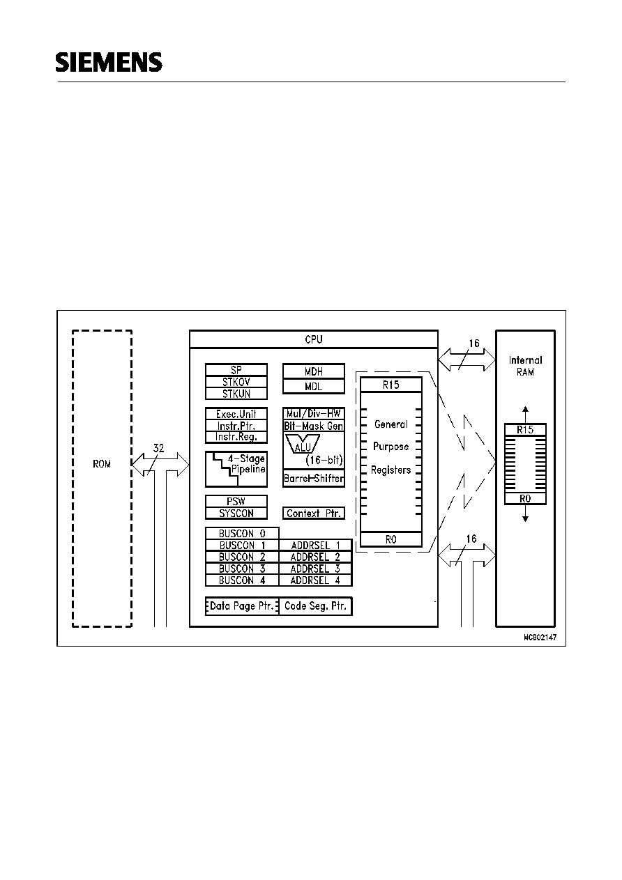
Central Processing Unit (CPU)
The main core of the CPU consists of a 4-stage instruction pipeline, a 16-bit arithmetic and logic unit
(ALU) and dedicated SFRs. Additional hardware has been spent for a separate multiply and divide
unit, a bit-mask generator and a barrel shifter.
Based on these hardware provisions, most of the C167CR-16RM's instructions can be executed in
just one machine cycle which requires 100 ns at 20-MHz CPU clock. For example, shift and rotate
instructions are always processed during one machine cycle independent of the number of bits to
be shifted. All multiple-cycle instructions have been optimized so that they can be executed very fast
as well: branches in 2 cycles, a 16
◊
16 bit multiplication in 5 cycles and a 32-/16 bit division in
10 cycles. Another pipeline optimization, the so-called `Jump Cache', allows reducing the execution
time of repeatedly performed jumps in a loop from 2 cycles to 1 cycle.
Figure 4
CPU Block Diagram

20Dec96@09:25h Intermediate Version
Semiconductor Group
14
C167CR-16RM
The CPU disposes of an actual register context consisting of up to 16 wordwide GPRs which are
physically allocated within the on-chip RAM area. A Context Pointer (CP) register determines the
base address of the active register bank to be accessed by the CPU at a time. The number of
register banks is only restricted by the available internal RAM space. For easy parameter passing,
a register bank may overlap others.
A system stack of up to 2048 bytes is provided as a storage for temporary data. The system stack
is allocated in the on-chip RAM area, and it is accessed by the CPU via the stack pointer (SP)
register. Two separate SFRs, STKOV and STKUN, are implicitly compared against the stack
pointer value upon each stack access for the detection of a stack overflow or underflow.
The high performance offered by the hardware implementation of the CPU can efficiently be utilized
by a programmer via the highly efficient C167CR-16RM instruction set which includes the following
instruction classes:
≠ Arithmetic Instructions
≠ Logical Instructions
≠ Boolean Bit Manipulation Instructions
≠ Compare and Loop Control Instructions
≠ Shift and Rotate Instructions
≠ Prioritize Instruction
≠ Data Movement Instructions
≠ System Stack Instructions
≠ Jump and Call Instructions
≠ Return Instructions
≠ System Control Instructions
≠ Miscellaneous Instructions
The basic instruction length is either 2 or 4 bytes. Possible operand types are bits, bytes and words.
A variety of direct, indirect or immediate addressing modes are provided to specify the required
operands.

20Dec96@09:25h Intermediate Version
15
Semiconductor Group
C167CR-16RM
Interrupt System
With an interrupt response time within a range from just 250 ns to 600 ns (in case of internal
program execution), the C167CR-16RM is capable of reacting very fast to the occurence of non-
deterministic events.
The architecture of the C167CR-16RM supports several mechanisms for fast and flexible response
to service requests that can be generated from various sources internal or external to the
microcontroller. Any of these interrupt requests can be programmed to being serviced by the
Interrupt Controller or by the Peripheral Event Controller (PEC).
In contrast to a standard interrupt service where the current program execution is suspended and
a branch to the interrupt vector table is performed, just one cycle is `stolen' from the current CPU
activity to perform a PEC service. A PEC service implies a single byte or word data transfer between
any two memory locations with an additional increment of either the PEC source or the destination
pointer. An individual PEC transfer counter is implicity decremented for each PEC service except
when performing in the continuous transfer mode. When this counter reaches zero, a standard
interrupt is performed to the corresponding source related vector location. PEC services are very
well suited, for example, for supporting the transmission or reception of blocks of data. The
C167CR-16RM has 8 PEC channels each of which offers such fast interrupt-driven data transfer
capabilities.
A separate control register which contains an interrupt request flag, an interrupt enable flag and an
interrupt priority bitfield exists for each of the possible interrupt sources. Via its related register, each
source can be programmed to one of sixteen interrupt priority levels. Once having been accepted
by the CPU, an interrupt service can only be interrupted by a higher prioritized service request. For
the standard interrupt processing, each of the possible interrupt sources has a dedicated vector
location.
Fast external interrupt inputs are provided to service external interrupts with high precision
requirements. These fast interrupt inputs feature programmable edge detection (rising edge, falling
edge or both edges).
Software interrupts are supported by means of the `TRAP' instruction in combination with an
individual trap (interrupt) number.
The following table shows all of the possible C167CR-16RM interrupt sources and the
corresponding hardware-related interrupt flags, vectors, vector locations and trap (interrupt)
numbers:
Note: Three nodes in the table (X-Peripheral nodes) are prepared to accept interrupt requests from
integrated X-Bus peripherals. Nodes, where no X-Peripherals are connected, may be used
to generate software controlled interrupt requests by setting the respective XPnIR bit.

20Dec96@09:25h Intermediate Version
Semiconductor Group
16
C167CR-16RM
Source of Interrupt or
PEC Service Request
Request
Flag
Enable
Flag
Interrupt
Vector
Vector
Location
Trap
Number
CAPCOM Register 0
CC0IR
CC0IE
CC0INT
00'0040
H
10
H
CAPCOM Register 1
CC1IR
CC1IE
CC1INT
00'0044
H
11
H
CAPCOM Register 2
CC2IR
CC2IE
CC2INT
00'0048
H
12
H
CAPCOM Register 3
CC3IR
CC3IE
CC3INT
00'004C
H
13
H
CAPCOM Register 4
CC4IR
CC4IE
CC4INT
00'0050
H
14
H
CAPCOM Register 5
CC5IR
CC5IE
CC5INT
00'0054
H
15
H
CAPCOM Register 6
CC6IR
CC6IE
CC6INT
00'0058
H
16
H
CAPCOM Register 7
CC7IR
CC7IE
CC7INT
00'005C
H
17
H
CAPCOM Register 8
CC8IR
CC8IE
CC8INT
00'0060
H
18
H
CAPCOM Register 9
CC9IR
CC9IE
CC9INT
00'0064
H
19
H
CAPCOM Register 10
CC10IR
CC10IE
CC10INT
00'0068
H
1A
H
CAPCOM Register 11
CC11IR
CC11IE
CC11INT
00'006C
H
1B
H
CAPCOM Register 12
CC12IR
CC12IE
CC12INT
00'0070
H
1C
H
CAPCOM Register 13
CC13IR
CC13IE
CC13INT
00'0074
H
1D
H
CAPCOM Register 14
CC14IR
CC14IE
CC14INT
00'0078
H
1E
H
CAPCOM Register 15
CC15IR
CC15IE
CC15INT
00'007C
H
1F
H
CAPCOM Register 16
CC16IR
CC16IE
CC16INT
00'00C0
H
30
H
CAPCOM Register 17
CC17IR
CC17IE
CC17INT
00'00C4
H
31
H
CAPCOM Register 18
CC18IR
CC18IE
CC18INT
00'00C8
H
32
H
CAPCOM Register 19
CC19IR
CC19IE
CC19INT
00'00CC
H
33
H
CAPCOM Register 20
CC20IR
CC20IE
CC20INT
00'00D0
H
34
H
CAPCOM Register 21
CC21IR
CC21IE
CC21INT
00'00D4
H
35
H
CAPCOM Register 22
CC22IR
CC22IE
CC22INT
00'00D8
H
36
H
CAPCOM Register 23
CC23IR
CC23IE
CC23INT
00'00DC
H
37
H
CAPCOM Register 24
CC24IR
CC24IE
CC24INT
00'00E0
H
38
H
CAPCOM Register 25
CC25IR
CC25IE
CC25INT
00'00E4
H
39
H
CAPCOM Register 26
CC26IR
CC26IE
CC26INT
00'00E8
H
3A
H
CAPCOM Register 27
CC27IR
CC27IE
CC27INT
00'00EC
H
3B
H
CAPCOM Register 28
CC28IR
CC28IE
CC28INT
00'00E0
H
3C
H
CAPCOM Register 29
CC29IR
CC29IE
CC29INT
00'0110
H
44
H
CAPCOM Register 30
CC30IR
CC30IE
CC30INT
00'0114
H
45
H
CAPCOM Register 31
CC31IR
CC31IE
CC31INT
00'0118
H
46
H
CAPCOM Timer 0
T0IR
T0IE
T0INT
00'0080
H
20
H

20Dec96@09:25h Intermediate Version
17
Semiconductor Group
C167CR-16RM
CAPCOM Timer 1
T1IR
T1IE
T1INT
00'0084
H
21
H
CAPCOM Timer 7
T7IR
T7IE
T7INT
00'00F4
H
3D
H
CAPCOM Timer 8
T8IR
T8IE
T8INT
00'00F8
H
3E
H
GPT1 Timer 2
T2IR
T2IE
T2INT
00'0088
H
22
H
GPT1 Timer 3
T3IR
T3IE
T3INT
00'008C
H
23
H
GPT1 Timer 4
T4IR
T4IE
T4INT
00'0090
H
24
H
GPT2 Timer 5
T5IR
T5IE
T5INT
00'0094
H
25
H
GPT2 Timer 6
T6IR
T6IE
T6INT
00'0098
H
26
H
GPT2 CAPREL Register
CRIR
CRIE
CRINT
00'009C
H
27
H
A/D Conversion Complete ADCIR
ADCIE
ADCINT
00'00A0
H
28
H
A/D Overrun Error
ADEIR
ADEIE
ADEINT
00'00A4
H
29
H
ASC0 Transmit
S0TIR
S0TIE
S0TINT
00'00A8
H
2A
H
ASC0 Transmit Buffer
S0TBIR
S0TBIE
S0TBINT
00'011C
H
47
H
ASC0 Receive
S0RIR
S0RIE
S0RINT
00'00AC
H
2B
H
ASC0 Error
S0EIR
S0EIE
S0EINT
00'00B0
H
2C
H
SSC Transmit
SCTIR
SCTIE
SCTINT
00'00B4
H
2D
H
SSC Receive
SCRIR
SCRIE
SCRINT
00'00B8
H
2E
H
SSC Error
SCEIR
SCEIE
SCEINT
00'00BC
H
2F
H
PWM Channel 0...3
PWMIR
PWMIE
PWMINT
00'00FC
H
3F
H
CAN Interface
XP0IR
XP0IE
XP0INT
00'0100
H
40
H
X-Peripheral Node
XP1IR
XP1IE
XP1INT
00'0104
H
41
H
X-Peripheral Node
XP2IR
XP2IE
XP2INT
00'0108
H
42
H
PLL Unlock
XP3IR
XP3IE
XP3INT
00'010C
H
43
H
Source of Interrupt or
PEC Service Request
Request
Flag
Enable
Flag
Interrupt
Vector
Vector
Location
Trap
Number
20Dec96@09:25h Intermediate Version
Semiconductor Group
18
C167CR-16RM
The C167CR-16RM also provides an excellent mechanism to identify and to process exceptions or
error conditions that arise during run-time, so-called `Hardware Traps'. Hardware traps cause
immediate non-maskable system reaction which is similar to a standard interrupt service (branching
to a dedicated vector table location). The occurence of a hardware trap is additionally signified by
an individual bit in the trap flag register (TFR). Except when another higher prioritized trap service
is in progress, a hardware trap will interrupt any actual program execution. In turn, hardware trap
services can normally not be interrupted by standard or PEC interrupts.
The following table shows all of the possible exceptions or error conditions that can arise during run-
time:
Exception Condition
Trap
Flag
Trap
Vector
Vector
Location
Trap
Number
Trap
Priority
Reset Functions:
Hardware Reset
Software Reset
Watchdog Timer Overflow
RESET
RESET
RESET
00'0000
H
00'0000
H
00'0000
H
00
H
00
H
00
H
III
III
III
Class A Hardware Traps:
Non-Maskable Interrupt
Stack Overflow
Stack Underflow
NMI
STKOF
STKUF
NMITRAP
STOTRAP
STUTRAP
00'0008
H
00'0010
H
00'0018
H
02
H
04
H
06
H
II
II
II
Class B Hardware Traps:
Undefined Opcode
Protected Instruction
Fault
Illegal Word Operand
Access
Illegal Instruction Access
Illegal External Bus
Access
UNDOPC
PRTFLT
ILLOPA
ILLINA
ILLBUS
BTRAP
BTRAP
BTRAP
BTRAP
BTRAP
00'0028
H
00'0028
H
00'0028
H
00'0028
H
00'0028
H
0A
H
0A
H
0A
H
0A
H
0A
H
I
I
I
I
I
Reserved
[2C
H
≠ 3C
H
] [0B
H
≠ 0F
H
]
Software Traps
TRAP Instruction
Any
[00'0000
H
≠
00'01FC
H
]
in steps
of 4
H
Any
[00
H
≠ 7F
H
]
Current
CPU
Priority
20Dec96@09:25h Intermediate Version
19
Semiconductor Group
C167CR-16RM
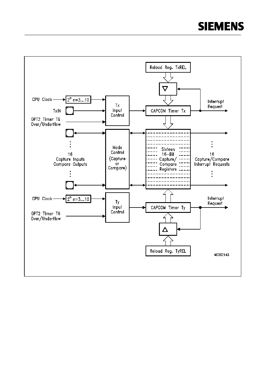
Capture/Compare (CAPCOM) Units
The CAPCOM units support generation and control of timing sequences on up to 32 channels with
a maximum resolution of 400 ns (at 20-MHz system clock). The CAPCOM units are typically used
to handle high speed I/O tasks such as pulse and waveform generation, pulse width modulation
(PMW), Digital to Analog (D/A) conversion, software timing, or time recording relative to external
events.
Four 16-bit timers (T0/T1, T7/T8) with reload registers provide two independent time bases for the
capture/compare register array.
The input clock for the timers is programmable to several prescaled values of the internal system
clock, or may be derived from an overflow/underflow of timer T6 in module GPT2. This provides a
wide range of variation for the timer period and resolution and allows precise adjustments to the
application specific requirements. In addition, external count inputs for CAPCOM timers T0 and T7
allow event scheduling for the capture/compare registers relative to external events.
Both of the two capture/compare register arrays contain 16 dual purpose capture/compare
registers, each of which may be individually allocated to either CAPCOM timer T0 or T1 (T7 or T8,
respectively), and programmed for capture or compare function. Each register has one port pin
associated with it which serves as an input pin for triggering the capture function, or as an output pin
(except for CC24...CC27) to indicate the occurence of a compare event.
When a capture/compare register has been selected for capture mode, the current contents of the
allocated timer will be latched (`capture'd) into the capture/compare register in response to an
external event at the port pin which is associated with this register. In addition, a specific interrupt
request for this capture/compare register is generated. Either a positive, a negative, or both a
positive and a negative external signal transition at the pin can be selected as the triggering event.
The contents of all registers which have been selected for one of the five compare modes are
continuously compared with the contents of the allocated timers. When a match occurs between the
timer value and the value in a capture/compare register, specific actions will be taken based on the
selected compare mode.
Compare Modes
Function
Mode 0
Interrupt-only compare mode;
several compare interrupts per timer period are possible
Mode 1
Pin toggles on each compare match;
several compare events per timer period are possible
Mode 2
Interrupt-only compare mode;
only one compare interrupt per timer period is generated
Mode 3
Pin set `1' on match; pin reset `0' on compare time overflow;
only one compare event per timer period is generated
Double
Register Mode
Two registers operate on one pin; pin toggles on each compare match;
several compare events per timer period are possible.
20Dec96@09:25h Intermediate Version
Semiconductor Group
20
C167CR-16RM
Figure 5
CAPCOM Unit Block Diagram
*)
*) 12 outputs on CAPCOM2

20Dec96@09:25h Intermediate Version
21
Semiconductor Group
C167CR-16RM
PWM Module
The Pulse Width Modulation Module can generate up to four PWM output signals using edge-
aligned or center-aligned PWM. In addition the PWM module can generate PWM burst signals and
single shot outputs. The frequency range of the PWM signals covers 4.8 Hz to 1 MHz (referred to
a CPU clock of 20 MHz), depending on the resolution of the PWM output signal. The level of the
output signals is selectable and the PWM module can generate interrupt requests.
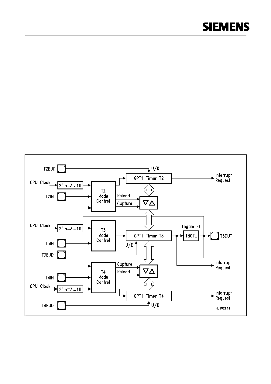
General Purpose Timer (GPT) Unit
The GPT unit represents a very flexible multifunctional timer/counter structure which may be used
for many different time related tasks such as event timing and counting, pulse width and duty cycle
measurements, pulse generation, or pulse multiplication.
The GPT unit incorporates five 16-bit timers which are organized in two separate modules, GPT1
and GPT2. Each timer in each module may operate independently in a number of different modes,
or may be concatenated with another timer of the same module.
Each of the three timers T2, T3, T4 of module GPT1 can be configured individually for one of four
basic modes of operation, which are Timer, Gated Timer, Counter, and Incremental Interface Mode.
In Timer Mode, the input clock for a timer is derived from the CPU clock, divided by a programmable
prescaler, while Counter Mode allows a timer to be clocked in reference to external events.
Pulse width or duty cycle measurement is supported in Gated Timer Mode, where the operation of
a timer is controlled by the `gate' level on an external input pin. For these purposes, each timer has
one associated port pin (TxIN) which serves as gate or clock input. The maximum resolution of the
timers in module GPT1 is 400 ns (@ 20-MHz CPU clock).
The count direction (up/down) for each timer is programmable by software or may additionally be
altered dynamically by an external signal on a port pin (TxEUD) to facilitate eg. position tracking.
In Incremental Interface Mode the GPT1 timers (T2, T3, T4) can be directly connected to the
incremental position sensor signals A and B via their respective inputs TxIN and TxEUD. Direction
and count signals are internally derived from these two input signals, so the contents of the
respective timer Tx corresponds to the sensor position. The third position sensor signal TOP0 can
be connected to an interrupt input.
Timers T3 and T4 have output toggle latches (TxOTL) which change their state on each timer over-
flow/underflow. The state of these latches may be output on port pins (TxOUT) eg. for time out
monitoring of external hardware components, or may be used internally to clock timers T2 and T4
for measuring long time periods with high resolution.
In addition to their basic operating modes, timers T2 and T4 may be configured as reload or capture
registers for timer T3. When used as capture or reload registers, timers T2 and T4 are stopped. The
contents of timer T3 is captured into T2 or T4 in response to a signal at their associated input pins
(TxIN). Timer T3 is reloaded with the contents of T2 or T4 triggered either by an external signal or
by a selectable state transition of its toggle latch T3OTL. When both T2 and T4 are configured to
alternately reload T3 on opposite state transitions of T3OTL with the low and high times of a PWM
signal, this signal can be constantly generated without software intervention.
With its maximum resolution of 200 ns (@ 20 MHz), the GPT2 module provides precise event
control and time measurement. It includes two timers (T5, T6) and a capture/reload register
20Dec96@09:25h Intermediate Version
Semiconductor Group
22
C167CR-16RM
(CAPREL). Both timers can be clocked with an input clock which is derived from the CPU clock via
a programmable prescaler or with external signals. The count direction (up/down) for each timer is
programmable by software or may additionally be altered dynamically by an external signal on a
port pin (TxEUD). Concatenation of the timers is supported via the output toggle latch (T6OTL) of
timer T6, which changes its state on each timer overflow/underflow.
The state of this latch may be used to clock timer T5, and/or it may be output on a port pin (T6OUT).
The overflows/underflows of timer T6 can additionally be used to clock the CAPCOM timers T0 or
T1, and to cause a reload from the CAPREL register. The CAPREL register may capture the
contents of timer T5 based on an external signal transition on the corresponding port pin (CAPIN),
and timer T5 may optionally be cleared after the capture procedure. This allows absolute time
differences to be measured or pulse multiplication to be performed without software overhead.
The capture trigger (timer T5 to CAPREL) may also be generated upon transitions of GPT1 timer
T3's inputs T3IN and/or T3EUD. This is especially advantageous when T3 operates in Incremental
Interface Mode.
Figure 6
Block Diagram of GPT1

20Dec96@09:25h Intermediate Version
23
Semiconductor Group
C167CR-16RM
Figure 7
Block Diagram of GPT2
Watchdog Timer
The Watchdog Timer represents one of the fail-safe mechanisms which have been implemented to
prevent the controller from malfunctioning for longer periods of time.
The Watchdog Timer is always enabled after a reset of the chip, and can only be disabled in the time
interval until the EINIT (end of initialization) instruction has been executed. Thus, the chip's start-up
procedure is always monitored. The software has to be designed to service the Watchdog Timer
before it overflows. If, due to hardware or software related failures, the software fails to do so, the
Watchdog Timer overflows and generates an internal hardware reset and pulls the RSTOUT pin low
in order to allow external hardware components to be reset.
The Watchdog Timer is a 16-bit timer, clocked with the system clock divided either by 2 or by 128.
The high byte of the Watchdog Timer register can be set to a prespecified reload value (stored in
WDTREL) in order to allow further variation of the monitored time interval. Each time it is serviced
by the application software, the high byte of the Watchdog Timer is reloaded. Thus, time intervals
between 25
µ
s and 420 ms can be monitored (@ 20 MHz). The default Watchdog Timer interval
after reset is 6.55 ms (@ 20 MHz).

20Dec96@09:25h Intermediate Version
Semiconductor Group
24
C167CR-16RM
A/D Converter
For analog signal measurement, a 10-bit A/D converter with 16 multiplexed input channels and a
sample and hold circuit has been integrated on-chip. It uses the method of successive
approximation. The sample time (for loading the capacitors) and the conversion time is
programmable and can so be adjusted to the external circuitry.
Overrun error detection/protection is provided for the conversion result register (ADDAT): either an
interrupt request will be generated when the result of a previous conversion has not been read from
the result register at the time the next conversion is complete, or the next conversion is suspended
in such a case until the previous result has been read.
For applications which require less than 16 analog input channels, the remaining channel inputs can
be used as digital input port pins.
The A/D converter of the C167CR-16RM supports four different conversion modes. In the standard
Single Channel conversion mode, the analog level on a specified channel is sampled once and
converted to a digital result. In the Single Channel Continuous mode, the analog level on a specified
channel is repeatedly sampled and converted without software intervention. In the Auto Scan mode,
the analog levels on a prespecified number of channels are sequentially sampled and converted. In
the Auto Scan Continuous mode, the number of prespecified channels is repeatedly sampled and
converted. In addition, the conversion of a specific channel can be inserted (injected) into a running
sequence without disturbing this sequence. This is called Channel Injection Mode.
The Peripheral Event Controller (PEC) may be used to automatically store the conversion results
into a table in memory for later evaluation, without requiring the overhead of entering and exiting
interrupt routines for each data transfer.
After each reset and also during normal operation the ADC automatically performs calibration
cycles. This automatic self-calibration constantly adjusts the converter to changing operating
conditions (eg. temperature) and compensates process variations.
These calibration cycles are part of the conversion cycle, so they do not affect the normal operation
of the A/D converter.

20Dec96@09:25h Intermediate Version
25
Semiconductor Group
C167CR-16RM
Serial Channels
Serial communication with other microcontrollers, processors, terminals or external peripheral
components is provided by two serial interfaces with different functionality, an Asynchronous/
Synchronous Serial Channel (ASC0) and a High-Speed Synchronous Serial Channel (SSC).
The ASC0 is upward compatible with the serial ports of the Siemens 8-bit microcontroller families
and supports full-duplex asynchronous communication at up to 625 KBaud and half-duplex
synchronous communication at up to 2.5 MBaud @ 20 MHz CPU clock.
A dedicated baud rate generator allows to set up all standard baud rates without oscillator tuning.
For transmission, reception and error handling 4 separate interrupt vectors are provided. In
asynchronous mode, 8- or 9-bit data frames are transmitted or received, preceded by a start bit and
terminated by one or two stop bits. For multiprocessor communication, a mechanism to distinguish
address from data bytes has been included (8-bit data plus wake up bit mode).
In synchronous mode, the ASC0 transmits or receives bytes (8 bits) synchronously to a shift clock
which is generated by the ASC0. The ASC0 always shifts the LSB first. A loop back option is
available for testing purposes.
A number of optional hardware error detection capabilities has been included to increase the
reliability of data transfers. A parity bit can automatically be generated on transmission or be
checked on reception. Framing error detection allows to recognize data frames with missing stop
bits. An overrun error will be generated, if the last character received has not been read out of the
receive buffer register at the time the reception of a new character is complete.
The SSC supports full-duplex synchronous communication at up to 5 Mbaud @ 20 MHz CPU clock.
It may be configured so it interfaces with serially linked peripheral components. A dedicated baud
rate generator allows to set up all standard baud rates without oscillator tuning. For transmission,
reception and error handling 3 separate interrupt vectors are provided.
The SSC transmits or receives characters of 2...16 bits length synchronously to a shift clock which
can be generated by the SSC (master mode) or by an external master (slave mode). The SSC can
start shifting with the LSB or with the MSB and allows the selection of shifting and latching clock
edges as well as the clock polarity.
A number of optional hardware error detection capabilities has been included to increase the
reliability of data transfers. Transmit and receive error supervise the correct handling of the data
buffer. Phase and baudrate error detect incorrect serial data.

20Dec96@09:25h Intermediate Version
Semiconductor Group
26
C167CR-16RM
CAN-Module
The integrated CAN-Module handles the completely autonomous transmission and reception of
CAN frames in accordance with the CAN specification V2.0 part B (active), ie. the on-chip CAN-
Module can receive and transmit standard frames with 11-bit identifiers as well as extended frames
with 29-bit identifiers.
The module provides Full CAN functionality on up to 15 message objects. Message object 15 may
be configured for Basic CAN functionality. Both modes provide separate masks for acceptance
filtering which allows to accept a number of identifiers in Full CAN mode and also allows to disregard
a number of identifiers in Basic CAN mode. All message objects can be updated independent from
the other objects and are equipped for the maximum message length of 8 bytes.
The bit timing is derived from the XCLK and is programmable up to a data rate of 1 MBaud. The
CAN-Module uses two pins of Port 4 to interface to a bus transceiver.
Note: When the CAN interface is to be used the segment address output on Port 4 must be limited
to 4 bits, ie. A19...A16. This is necessary to enable the alternate function of the CAN
interface pins.
Parallel Ports
The C167CR-16RM provides up to 111 I/O lines which are organized into eight input/output ports
and one input port. All port lines are bit-addressable, and all input/output lines are individually (bit-
wise) programmable as inputs or outputs via direction registers. The I/O ports are true bidirectional
ports which are switched to high impedance state when configured as inputs. The output drivers of
five I/O ports can be configured (pin by pin) for push/pull operation or open-drain operation via
control registers. During the internal reset, all port pins are configured as inputs.
The input threshold of Port 2, Port 3, Port 7 and Port 8 is selectable (TTL or CMOS like), where the
special CMOS like input threshold reduces noise sensitivity due to the input hysteresis. The input
threshold may be selected individually for each byte of the respective ports.
All port lines have programmable alternate input or output functions associated with them.
PORT0 and PORT1 may be used as address and data lines when accessing external memory,
while Port 4 outputs the additional segment address bits A23/19/17...A16 in systems where
segmentation is enabled to access more than 64 KBytes of memory.
Port 2, Port 8 and Port 7 are associated with the capture inputs or compare outputs of the CAPCOM
units and/or with the outputs of the PWM module.
Port 6 provides optional bus arbitration signals (BREQ, HLDA, HOLD) and chip select signals.
Port 3 includes alternate functions of timers, serial interfaces, the optional bus control signal BHE
and the system clock output (CLKOUT).
Port 5 is used for the analog input channels to the A/D converter or timer control signals.
All port lines that are not used for these alternate functions may be used as general purpose IO
lines.

20Dec96@09:25h Intermediate Version
27
Semiconductor Group
C167CR-16RM
Instruction Set Summary
The table below lists the instructions of the C167CR-16RM in a condensed way.
The various addressing modes that can be used with a specific instruction, the operation of the
instructions, parameters for conditional execution of instructions, and the opcodes for each
instruction can be found in the "C16x Family Instruction Set Manual".
This document also provides a detailled description of each instruction.
Instruction Set Summary
Mnemonic
Description
Bytes
ADD(B)
Add word (byte) operands
2 / 4
ADDC(B)
Add word (byte) operands with Carry
2 / 4
SUB(B)
Subtract word (byte) operands
2 / 4
SUBC(B)
Subtract word (byte) operands with Carry
2 / 4
MUL(U)
(Un)Signed multiply direct GPR by direct GPR (16-16-bit)
2
DIV(U)
(Un)Signed divide register MDL by direct GPR (16-/16-bit)
2
DIVL(U)
(Un)Signed long divide reg. MD by direct GPR (32-/16-bit)
2
CPL(B)
Complement direct word (byte) GPR
2
NEG(B)
Negate direct word (byte) GPR
2
AND(B)
Bitwise AND, (word/byte operands)
2 / 4
OR(B)
Bitwise OR, (word/byte operands)
2 / 4
XOR(B)
Bitwise XOR, (word/byte operands)
2 / 4
BCLR
Clear direct bit
2
BSET
Set direct bit
2
BMOV(N)
Move (negated) direct bit to direct bit
4
BAND, BOR, BXOR
AND/OR/XOR direct bit with direct bit
4
BCMP
Compare direct bit to direct bit
4
BFLDH/L
Bitwise modify masked high/low byte of bit-addressable
direct word memory with immediate data
4
CMP(B)
Compare word (byte) operands
2 / 4
CMPD1/2
Compare word data to GPR and decrement GPR by 1/2
2 / 4
CMPI1/2
Compare word data to GPR and increment GPR by 1/2
2 / 4
PRIOR
Determine number of shift cycles to normalize direct
word GPR and store result in direct word GPR
2
SHL / SHR
Shift left/right direct word GPR
2
ROL / ROR
Rotate left/right direct word GPR
2
ASHR
Arithmetic (sign bit) shift right direct word GPR
2
20Dec96@09:25h Intermediate Version
Semiconductor Group
28
C167CR-16RM
MOV(B)
Move word (byte) data
2 / 4
MOVBS
Move byte operand to word operand with sign extension
2 / 4
MOVBZ
Move byte operand to word operand. with zero extension
2 / 4
JMPA, JMPI, JMPR
Jump absolute/indirect/relative if condition is met
4
JMPS
Jump absolute to a code segment
4
J(N)B
Jump relative if direct bit is (not) set
4
JBC
Jump relative and clear bit if direct bit is set
4
JNBS
Jump relative and set bit if direct bit is not set
4
CALLA, CALLI, CALLR
Call absolute/indirect/relative subroutine if condition is met
4
CALLS
Call absolute subroutine in any code segment
4
PCALL
Push direct word register onto system stack and call
absolute subroutine
4
TRAP
Call interrupt service routine via immediate trap number
2
PUSH, POP
Push/pop direct word register onto/from system stack
2
SCXT
Push direct word register onto system stack und update
register with word operand
4
RET
Return from intra-segment subroutine
2
RETS
Return from inter-segment subroutine
2
RETP
Return from intra-segment subroutine and pop direct
word register from system stack
2
RETI
Return from interrupt service subroutine
2
SRST
Software Reset
4
IDLE
Enter Idle Mode
4
PWRDN
Enter Power Down Mode
(supposes NMI-pin being low)
4
SRVWDT
Service Watchdog Timer
4
DISWDT
Disable Watchdog Timer
4
EINIT
Signify End-of-Initialization on RSTOUT-pin
4
ATOMIC
Begin ATOMIC sequence
2
EXTR
Begin EXTended Register sequence
2
EXTP(R)
Begin EXTended Page (and Register) sequence
2 / 4
EXTS(R)
Begin EXTended Segment (and Register) sequence
2 / 4
NOP
Null operation
2
Instruction Set Summary (cont'd)
Mnemonic
Description
Bytes

20Dec96@09:25h Intermediate Version
29
Semiconductor Group
C167CR-16RM
Special Function Registers Overview
The following table lists all SFRs which are implemented in the C167CR-16RM in alphabetical
order.
Bit-addressable SFRs are marked with the letter "b" in column "Name". SFRs within the Extended
SFR-Space (ESFRs) are marked with the letter "E" in column "Physical Address".
An SFR can be specified via its individual mnemonic name. Depending on the selected addressing
mode, an SFR can be accessed via its physical address (using the Data Page Pointers), or via its
short 8-bit address (without using the Data Page Pointers).
Special Function Registers Overview
Name
Physical
Address
8-Bit
Address
Description
Reset
Value
ADCIC
b FF98
H
CC
H
A/D Converter End of Conversion Interrupt
Control Register
0000
H
ADCON
b FFA0
H
D0
H
A/D Converter Control Register
0000
H
ADDAT
FEA0
H
50
H
A/D Converter Result Register
0000
H
ADDAT2
F0A0
H
E 50
H
A/D Converter 2 Result Register
0000
H
ADDRSEL1
FE18
H
0C
H
Address Select Register 1
0000
H
ADDRSEL2
FE1A
H
0D
H
Address Select Register 2
0000
H
ADDRSEL3
FE1C
H
0E
H
Address Select Register 3
0000
H
ADDRSEL4
FE1E
H
0F
H
Address Select Register 4
0000
H
ADEIC
b FF9A
H
CD
H
A/D Converter Overrun Error Interrupt Control
Register
0000
H
BUSCON0 b FF0C
H
86
H
Bus Configuration Register 0
0XX0
H
BUSCON1 b FF14
H
8A
H
Bus Configuration Register 1
0000
H
BUSCON2 b FF16
H
8B
H
Bus Configuration Register 2
0000
H
BUSCON3 b FF18
H
8C
H
Bus Configuration Register 3
0000
H
BUSCON4 b FF1A
H
8D
H
Bus Configuration Register 4
0000
H
CAPREL
FE4A
H
25
H
GPT2 Capture/Reload Register
0000
H
CC0
FE80
H
40
H
CAPCOM Register 0
0000
H
CC0IC
b FF78
H
BC
H
CAPCOM Register 0 Interrupt Control Register
0000
H
CC1
FE82
H
41
H
CAPCOM Register 1
0000
H
CC1IC
b FF7A
H
BD
H
CAPCOM Register 1 Interrupt Control Register
0000
H
CC2
FE84
H
42
H
CAPCOM Register 2
0000
H
CC2IC
b FF7C
H
BE
H
CAPCOM Register 2 Interrupt Control Register
0000
H
20Dec96@09:25h Intermediate Version
Semiconductor Group
30
C167CR-16RM
CC3
FE86
H
43
H
CAPCOM Register 3
0000
H
CC3IC
b FF7E
H
BF
H
CAPCOM Register 3 Interrupt Control Register
0000
H
CC4
FE88
H
44
H
CAPCOM Register 4
0000
H
CC4IC
b FF80
H
C0
H
CAPCOM Register 4 Interrupt Control Register
0000
H
CC5
FE8A
H
45
H
CAPCOM Register 5
0000
H
CC5IC
b FF82
H
C1
H
CAPCOM Register 5 Interrupt Control Register
0000
H
CC6
FE8C
H
46
H
CAPCOM Register 6
0000
H
CC6IC
b FF84
H
C2
H
CAPCOM Register 6 Interrupt Control Register
0000
H
CC7
FE8E
H
47
H
CAPCOM Register 7
0000
H
CC7IC
b FF86
H
C3
H
CAPCOM Register 7 Interrupt Control Register
0000
H
CC8
FE90
H
48
H
CAPCOM Register 8
0000
H
CC8IC
b FF88
H
C4
H
CAPCOM Register 8 Interrupt Control Register
0000
H
CC9
FE92
H
49
H
CAPCOM Register 9
0000
H
CC9IC
b FF8A
H
C5
H
CAPCOM Register 9 Interrupt Control Register
0000
H
CC10
FE94
H
4A
H
CAPCOM Register 10
0000
H
CC10IC
b FF8C
H
C6
H
CAPCOM Register 10 Interrupt Control Register
0000
H
CC11
FE96
H
4B
H
CAPCOM Register 11
0000
H
CC11IC
b FF8E
H
C7
H
CAPCOM Register 11 Interrupt Control Register
0000
H
CC12
FE98
H
4C
H
CAPCOM Register 12
0000
H
CC12IC
b FF90
H
C8
H
CAPCOM Register 12 Interrupt Control Register
0000
H
CC13
FE9A
H
4D
H
CAPCOM Register 13
0000
H
CC13IC
b FF92
H
C9
H
CAPCOM Register 13 Interrupt Control Register
0000
H
CC14
FE9C
H
4E
H
CAPCOM Register 14
0000
H
CC14IC
b FF94
H
CA
H
CAPCOM Register 14 Interrupt Control Register
0000
H
CC15
FE9E
H
4F
H
CAPCOM Register 15
0000
H
CC15IC
b FF96
H
CB
H
CAPCOM Register 15 Interrupt Control Register
0000
H
CC16
FE60
H
30
H
CAPCOM Register 16
0000
H
CC16IC
b F160
H
E B0
H
CAPCOM Register 16 Interrupt Control Register
0000
H
CC17
FE62
H
31
H
CAPCOM Register 17
0000
H
Special Function Registers Overview (cont'd)
Name
Physical
Address
8-Bit
Address
Description
Reset
Value

20Dec96@09:25h Intermediate Version
31
Semiconductor Group
C167CR-16RM
CC17IC
b F162
H
E B1
H
CAPCOM Register 17 Interrupt Control Register
0000
H
CC18
FE64
H
32
H
CAPCOM Register 18
0000
H
CC18IC
b F164
H
E B2
H
CAPCOM Register 18 Interrupt Control Register
0000
H
CC19
FE66
H
33
H
CAPCOM Register 19
0000
H
CC19IC
b F166
H
E B3
H
CAPCOM Register 19 Interrupt Control Register
0000
H
CC20
FE68
H
34
H
CAPCOM Register 20
0000
H
CC20IC
b F168
H
E B4
H
CAPCOM Register 20 Interrupt Control Register
0000
H
CC21
FE6A
H
35
H
CAPCOM Register 21
0000
H
CC21IC
b F16A
H
E B5
H
CAPCOM Register 21 Interrupt Control Register
0000
H
CC22
FE6C
H
36
H
CAPCOM Register 22
0000
H
CC22IC
b F16C
H
E B6
H
CAPCOM Register 22 Interrupt Control Register
0000
H
CC23
FE6E
H
37
H
CAPCOM Register 23
0000
H
CC23IC
b F16E
H
E B7
H
CAPCOM Register 23 Interrupt Control Register
0000
H
CC24
FE70
H
38
H
CAPCOM Register 24
0000
H
CC24IC
b F170
H
E B8
H
CAPCOM Register 24 Interrupt Control Register
0000
H
CC25
FE72
H
39
H
CAPCOM Register 25
0000
H
CC25IC
b F172
H
E B9
H
CAPCOM Register 25 Interrupt Control Register
0000
H
CC26
FE74
H
3A
H
CAPCOM Register 26
0000
H
CC26IC
b F174
H
E BA
H
CAPCOM Register 26 Interrupt Control Register
0000
H
CC27
FE76
H
3B
H
CAPCOM Register 27
0000
H
CC27IC
b F176
H
E BB
H
CAPCOM Register 27 Interrupt Control Register
0000
H
CC28
FE78
H
3C
H
CAPCOM Register 28
0000
H
CC28IC
b F178
H
E BC
H
CAPCOM Register 28 Interrupt Control Register
0000
H
CC29
FE7A
H
3D
H
CAPCOM Register 29
0000
H
CC29IC
b F184
H
E C2
H
CAPCOM Register 29 Interrupt Control Register
0000
H
CC30
FE7C
H
3E
H
CAPCOM Register 30
0000
H
CC30IC
b F18C
H
E C6
H
CAPCOM Register 30 Interrupt Control Register
0000
H
CC31
FE7E
H
3F
H
CAPCOM Register 31
0000
H
CC31IC
b F194
H
E CA
H
CAPCOM Register 31 Interrupt Control Register
0000
H
Special Function Registers Overview (cont'd)
Name
Physical
Address
8-Bit
Address
Description
Reset
Value

20Dec96@09:25h Intermediate Version
Semiconductor Group
32
C167CR-16RM
CCM0
b FF52
H
A9
H
CAPCOM Mode Control Register 0
0000
H
CCM1
b FF54
H
AA
H
CAPCOM Mode Control Register 1
0000
H
CCM2
b FF56
H
AB
H
CAPCOM Mode Control Register 2
0000
H
CCM3
b FF58
H
AC
H
CAPCOM Mode Control Register 3
0000
H
CCM4
b FF22
H
91
H
CAPCOM Mode Control Register 4
0000
H
CCM5
b FF24
H
92
H
CAPCOM Mode Control Register 5
0000
H
CCM6
b FF26
H
93
H
CAPCOM Mode Control Register 6
0000
H
CCM7
b FF28
H
94
H
CAPCOM Mode Control Register 7
0000
H
CP
FE10
H
08
H
CPU Context Pointer Register
FC00
H
CRIC
b FF6A
H
B5
H
GPT2 CAPREL Interrupt Control Register
0000
H
CSP
FE08
H
04
H
CPU Code Segment Pointer Register (read only)
0000
H
DP0L
b F100
H
E 80
H
P0L Direction Control Register
00
H
DP0H
b F102
H
E 81
H
P0H Direction Control Register
00
H
DP1L
b F104
H
E 82
H
P1L Direction Control Register
00
H
DP1H
b F106
H
E 83
H
P1H Direction Control Register
00
H
DP2
b FFC2
H
E1
H
Port 2 Direction Control Register
0000
H
DP3
b FFC6
H
E3
H
Port 3 Direction Control Register
0000
H
DP4
b FFCA
H
E5
H
Port 4 Direction Control Register
00
H
DP6
b FFCE
H
E7
H
Port 6 Direction Control Register
00
H
DP7
b FFD2
H
E9
H
Port 7 Direction Control Register
00
H
DP8
b FFD6
H
EB
H
Port 8 Direction Control Register
00
H
DPP0
FE00
H
00
H
CPU Data Page Pointer 0 Register (10 bits)
0000
H
DPP1
FE02
H
01
H
CPU Data Page Pointer 1 Register (10 bits)
0001
H
DPP2
FE04
H
02
H
CPU Data Page Pointer 2 Register (10 bits)
0002
H
DPP3
FE06
H
03
H
CPU Data Page Pointer 3 Register (10 bits)
0003
H
EXICON
b F1C0
H
E E0
H
External Interrupt Control Register
0000
H
MDC
b FF0E
H
87
H
CPU Multiply Divide Control Register
0000
H
MDH
FE0C
H
06
H
CPU Multiply Divide Register ≠ High Word
0000
H
MDL
FE0E
H
07
H
CPU Multiply Divide Register ≠ Low Word
0000
H
Special Function Registers Overview (cont'd)
Name
Physical
Address
8-Bit
Address
Description
Reset
Value

20Dec96@09:25h Intermediate Version
33
Semiconductor Group
C167CR-16RM
ODP2
b F1C2
H
E E1
H
Port 2 Open Drain Control Register
0000
H
ODP3
b F1C6
H
E E3
H
Port 3 Open Drain Control Register
0000
H
ODP6
b F1CE
H
E E7
H
Port 6 Open Drain Control Register
00
H
ODP7
b F1D2
H
E E9
H
Port 7 Open Drain Control Register
00
H
ODP8
b F1D6
H
E EB
H
Port 8 Open Drain Control Register
00
H
ONES
FF1E
H
8F
H
Constant Value 1's Register (read only)
FFFF
H
P0L
b FF00
H
80
H
Port 0 Low Register (Lower half of PORT0)
00
H
P0H
b FF02
H
81
H
Port 0 High Register (Upper half of PORT0)
00
H
P1L
b FF04
H
82
H
Port 1 Low Register (Lower half of PORT1)
00
H
P1H
b FF06
H
83
H
Port 1 High Register (Upper half of PORT1)
00
H
P2
b FFC0
H
E0
H
Port 2 Register
0000
H
P3
b FFC4
H
E2
H
Port 3 Register
0000
H
P4
b FFC8
H
E4
H
Port 4 Register (8 bits)
00
H
P5
b FFA2
H
D1
H
Port 5 Register (read only)
XXXX
H
P6
b FFCC
H
E6
H
Port 6 Register (8 bits)
00
H
P7
b FFD0
H
E8
H
Port 7 Register (8 bits)
00
H
P8
b FFD4
H
EA
H
Port 8 Register (8 bits)
00
H
PECC0
FEC0
H
60
H
PEC Channel 0 Control Register
0000
H
PECC1
FEC2
H
61
H
PEC Channel 1 Control Register
0000
H
PECC2
FEC4
H
62
H
PEC Channel 2 Control Register
0000
H
PECC3
FEC6
H
63
H
PEC Channel 3 Control Register
0000
H
PECC4
FEC8
H
64
H
PEC Channel 4 Control Register
0000
H
PECC5
FECA
H
65
H
PEC Channel 5 Control Register
0000
H
PECC6
FECC
H
66
H
PEC Channel 6 Control Register
0000
H
PECC7
FECE
H
67
H
PEC Channel 7 Control Register
0000
H
PICON
F1C4
H
E E2
H
Port Input Threshold Control Register
0000
H
PP0
F038
H
E 1C
H
PWM Module Period Register 0
0000
H
PP1
F03A
H
E 1D
H
PWM Module Period Register 1
0000
H
PP2
F03C
H
E 1E
H
PWM Module Period Register 2
0000
H
Special Function Registers Overview (cont'd)
Name
Physical
Address
8-Bit
Address
Description
Reset
Value

20Dec96@09:25h Intermediate Version
Semiconductor Group
34
C167CR-16RM
PP3
F03E
H
E 1F
H
PWM Module Period Register 3
0000
H
PSW
b FF10
H
88
H
CPU Program Status Word
0000
H
PT0
F030
H
E 18
H
PWM Module Up/Down Counter 0
0000
H
PT1
F032
H
E 19
H
PWM Module Up/Down Counter 1
0000
H
PT2
F034
H
E 1A
H
PWM Module Up/Down Counter 2
0000
H
PT3
F036
H
E 1B
H
PWM Module Up/Down Counter 3
0000
H
PW0
FE30
H
18
H
PWM Module Pulse Width Register 0
0000
H
PW1
FE32
H
19
H
PWM Module Pulse Width Register 1
0000
H
PW2
FE34
H
1A
H
PWM Module Pulse Width Register 2
0000
H
PW3
FE36
H
1B
H
PWM Module Pulse Width Register 3
0000
H
PWMCON0 b FF30
H
98
H
PWM Module Control Register 0
0000
H
PWMCON1 b FF32
H
99
H
PWM Module Control Register 1
0000
H
PWMIC
b F17E
H
E BF
H
PWM Module Interrupt Control Register
0000
H
RP0H
b F108
H
E 84
H
System Startup Configuration Register (Rd. only)
XX
H
S0BG
FEB4
H
5A
H
Serial Channel 0 Baud Rate Generator Reload
Register
0000
H
S0CON
b FFB0
H
D8
H
Serial Channel 0 Control Register
0000
H
S0EIC
b FF70
H
B8
H
Serial Channel 0 Error Interrupt Control Register
0000
H
S0RBUF
FEB2
H
59
H
Serial Channel 0 Receive Buffer Register
(read only)
XX
H
S0RIC
b FF6E
H
B7
H
Serial Channel 0 Receive Interrupt Control
Register
0000
H
S0TBIC
b F19C
H
E CE
H
Serial Channel 0 Transmit Buffer Interrupt Control
Register
0000
H
S0TBUF
FEB0
H
58
H
Serial Channel 0 Transmit Buffer Register
(write only)
00
H
S0TIC
b FF6C
H
B6
H
Serial Channel 0 Transmit Interrupt Control
Register
0000
H
SP
FE12
H
09
H
CPU System Stack Pointer Register
FC00
H
SSCBR
F0B4
H
E 5A
H
SSC Baudrate Register
0000
H
SSCCON
b FFB2
H
D9
H
SSC Control Register
0000
H
Special Function Registers Overview (cont'd)
Name
Physical
Address
8-Bit
Address
Description
Reset
Value

20Dec96@09:25h Intermediate Version
35
Semiconductor Group
C167CR-16RM
SSCEIC
b FF76
H
BB
H
SSC Error Interrupt Control Register
0000
H
SSCRB
F0B2
H
E 59
H
SSC Receive Buffer (read only)
XXXX
H
SSCRIC
b FF74
H
BA
H
SSC Receive Interrupt Control Register
0000
H
SSCTB
F0B0
H
E 58
H
SSC Transmit Buffer (write only)
0000
H
SSCTIC
b FF72
H
B9
H
SSC Transmit Interrupt Control Register
0000
H
STKOV
FE14
H
0A
H
CPU Stack Overflow Pointer Register
FA00
H
STKUN
FE16
H
0B
H
CPU Stack Underflow Pointer Register
FC00
H
SYSCON
b FF12
H
89
H
CPU System Configuration Register
0xx0
H
1)
T0
FE50
H
28
H
CAPCOM Timer 0 Register
0000
H
T01CON
b FF50
H
A8
H
CAPCOM Timer 0 and Timer 1 Control Register
0000
H
T0IC
b FF9C
H
CE
H
CAPCOM Timer 0 Interrupt Control Register
0000
H
T0REL
FE54
H
2A
H
CAPCOM Timer 0 Reload Register
0000
H
T1
FE52
H
29
H
CAPCOM Timer 1 Register
0000
H
T1IC
b FF9E
H
CF
H
CAPCOM Timer 1 Interrupt Control Register
0000
H
T1REL
FE56
H
2B
H
CAPCOM Timer 1 Reload Register
0000
H
T2
FE40
H
20
H
GPT1 Timer 2 Register
0000
H
T2CON
b FF40
H
A0
H
GPT1 Timer 2 Control Register
0000
H
T2IC
b FF60
H
B0
H
GPT1 Timer 2 Interrupt Control Register
0000
H
T3
FE42
H
21
H
GPT1 Timer 3 Register
0000
H
T3CON
b FF42
H
A1
H
GPT1 Timer 3 Control Register
0000
H
T3IC
b FF62
H
B1
H
GPT1 Timer 3 Interrupt Control Register
0000
H
T4
FE44
H
22
H
GPT1 Timer 4 Register
0000
H
T4CON
b FF44
H
A2
H
GPT1 Timer 4 Control Register
0000
H
T4IC
b FF64
H
B2
H
GPT1 Timer 4 Interrupt Control Register
0000
H
T5
FE46
H
23
H
GPT2 Timer 5 Register
0000
H
T5CON
b FF46
H
A3
H
GPT2 Timer 5 Control Register
0000
H
T5IC
b FF66
H
B3
H
GPT2 Timer 5 Interrupt Control Register
0000
H
T6
FE48
H
24
H
GPT2 Timer 6 Register
0000
H
T6CON
b FF48
H
A4
H
GPT2 Timer 6 Control Register
0000
H
Special Function Registers Overview (cont'd)
Name
Physical
Address
8-Bit
Address
Description
Reset
Value

20Dec96@09:25h Intermediate Version
Semiconductor Group
36
C167CR-16RM
1)
The system configuration is selected during reset.
2)
Bit WDTR indicates a watchdog timer triggered reset.
Note: The Interrupt Control Registers XPnIC are prepared to control interrupt requests from
integrated X-Bus peripherals. Nodes, where no X-Peripherals are connected, may be used
to generate software controlled interrupt requests by setting the respective XPnIR bit.
T6IC
b FF68
H
B4
H
GPT2 Timer 6 Interrupt Control Register
0000
H
T7
F050
H
E 28
H
CAPCOM Timer 7 Register
0000
H
T78CON
b FF20
H
90
H
CAPCOM Timer 7 and 8 Control Register
0000
H
T7IC
b F17A
H
E BE
H
CAPCOM Timer 7 Interrupt Control Register
0000
H
T7REL
F054
H
E 2A
H
CAPCOM Timer 7 Reload Register
0000
H
T8
F052
H
E 29
H
CAPCOM Timer 8 Register
0000
H
T8IC
b F17C
H
E BF
H
CAPCOM Timer 8 Interrupt Control Register
0000
H
T8REL
F056
H
E 2B
H
CAPCOM Timer 8 Reload Register
0000
H
TFR
b FFAC
H
D6
H
Trap Flag Register
0000
H
WDT
FEAE
H
57
H
Watchdog Timer Register (read only)
0000
H
WDTCON
FFAE
H
D7
H
Watchdog Timer Control Register
000X
H
2)
XP0IC
b F186
H
E C3
H
CAN Module Interrupt Control Register
0000
H
XP1IC
b F18E
H
E C7
H
X-Peripheral 1 Interrupt Control Register
0000
H
XP2IC
b F196
H
E CB
H
X-Peripheral 2 Interrupt Control Register
0000
H
XP3IC
b F19E
H
E CF
H
PLL Interrupt Control Register
0000
H
ZEROS
b FF1C
H
8E
H
Constant Value 0's Register (read only)
0000
H
Special Function Registers Overview (cont'd)
Name
Physical
Address
8-Bit
Address
Description
Reset
Value

20Dec96@09:25h Intermediate Version
37
Semiconductor Group
C167CR-16RM
Absolute Maximum Ratings
Ambient temperature under bias (
T
A
):
SAB-C167CR-16RM ........................................................................................................0 to +70 ∞C
SAF-C167CR-16RM .................................................................................................... ≠40 to +85 ∞C
SAK-C167CR-16RM .................................................................................................. ≠40 to +125 ∞C
Storage temperature (
T
ST
)......................................................................................... ≠ 65 to +150 ∞C
Voltage on
V
CC
pins with respect to ground (
V
SS
) ....................................................... ≠0.5 to +6.5 V
Voltage on any pin with respect to ground (
V
SS
) ...................................................≠0.5 to
V
CC
+0.5 V
Input current on any pin during overload condition .................................................... ≠10 to +10 mA
Absolute sum of all input currents during overload condition ..............................................|100 mA|
Power dissipation..................................................................................................................... 1.5 W
Note: Stresses above those listed under "Absolute Maximum Ratings" may cause permanent
damage to the device. This is a stress rating only and functional operation of the device at
these or any other conditions above those indicated in the operational sections of this
specification is not implied. Exposure to absolute maximum rating conditions for extended
periods may affect device reliability. During overload conditions (
V
IN
>
V
CC
or
V
IN
<
V
SS
) the
voltage on pins with respect to ground (
V
SS
) must not exceed the values defined by the
Absolute Maximum Ratings.
Parameter Interpretation
The parameters listed in the following partly represent the characteristics of the C167CR-16RM and
partly its demands on the system. To aid in interpreting the parameters right, when evaluating them
for a design, they are marked in column "Symbol":
CC (Controller Characteristics):
The logic of the C167CR-16RM will provide signals with the respective timing characteristics.
SR (System Requirement):
The external system must provide signals with the respective timing characteristics to the C167CR-
16RM.
20Dec96@09:25h Intermediate Version
Semiconductor Group
38
C167CR-16RM
DC Characteristics
V
CC
= 5 V
±
10 %;
V
SS
= 0 V;
f
CPU
= 20 MHz
T
A
= 0 to +70 ∞C
for SAB-C167CR-16RM
T
A
= -40 to +85 ∞C
for SAF-C167CR-16RM
T
A
= -40 to +125 ∞C
for SAK-C167CR-16RM
Parameter
Symbol
Limit Values
Unit
Test Condition
min.
max.
Input low voltage
(TTL)
V
IL
SR ≠ 0.5
0.2
V
CC
≠ 0.1
V
≠
Input low voltage
(Special Threshold)
V
ILS
SR ≠ 0.5
2.0
V
≠
Input high voltage, all except
RSTIN and XTAL1 (TTL)
V
IH
SR 0.2
V
CC
+ 0.9
V
CC
+ 0.5
V
≠
Input high voltage RSTIN
V
IH1
SR 0.6
V
CC
V
CC
+ 0.5
V
≠
Input high voltage XTAL1
V
IH2
SR 0.7
V
CC
V
CC
+ 0.5
V
≠
Input high voltage
(Special Threshold)
V
IHS
SR 0.8
V
CC
- 0.2
V
CC
+ 0.5
V
≠
Input Hysteresis
(Special Threshold)
HYS
400
-
mV
≠
Output low voltage
(PORT0, PORT1, Port 4, ALE, RD,
WR, BHE, CLKOUT, RSTOUT)
V
OL
CC ≠
0.45
V
I
OL
= 2.4 mA
Output low voltage
(all other outputs)
V
OL1
CC ≠
0.45
V
I
OL1
= 1.6 mA
Output high voltage
(PORT0, PORT1, Port 4, ALE, RD,
WR, BHE, CLKOUT, RSTOUT)
V
OH
CC 0.9
V
CC
2.4
≠
V
I
OH
= ≠ 500
µ
A
I
OH
= ≠ 2.4 mA
Output high voltage
1)
(all other outputs)
V
OH1
CC 0.9
V
CC
2.4
≠
V
V
I
OH
= ≠ 250
µ
A
I
OH
= ≠ 1.6 mA
Input leakage current (Port 5)
I
OZ1
CC ≠
±
200
nA
0.45V <
V
IN
<
V
CC
Input leakage current (all other)
I
OZ2
CC ≠
±
500
nA
0.45V <
V
IN
<
V
CC
Overload current
I
OV
SR ≠
±
5
mA
5) 8)
RSTIN pullup resistor
R
RST
CC 50
250
k
≠
Read/Write inactive current
4)
I
RWH
2)
≠
-40
µ
A
V
OUT
= 2.4 V
Read/Write active current
4)
I
RWL
3)
-500
≠
µ
A
V
OUT
=
V
OLmax
ALE inactive current
4)
I
ALEL
2)
≠
40
µ
A
V
OUT
=
V
OLmax
ALE active current
4)
I
ALEH
3)
500
≠
µ
A
V
OUT
= 2.4 V
Port 6 inactive current
4)
I
P6H
2)
≠
-40
µ
A
V
OUT
= 2.4 V
20Dec96@09:25h Intermediate Version
39
Semiconductor Group
C167CR-16RM
Notes
1)
This specification is not valid for outputs which are switched to open drain mode. In this case the respective
output will float and the voltage results from the external circuitry.
2)
The maximum current may be drawn while the respective signal line remains inactive.
3)
The minimum current must be drawn in order to drive the respective signal line active.
4)
This specification is only valid during Reset, or during Hold- or Adapt-mode. Port 6 pins are only affected, if
they are used for CS output and the open drain function is not enabled.
5)
Not 100% tested, guaranteed by design characterization.
6)
The supply current is a function of the operating frequency. This dependency is illustrated in the figure below.
These parameters are tested at
V
CCmax
and 20 MHz CPU clock with all outputs disconnected and all inputs
at
V
IL
or
V
IH
.
7)
This parameter is tested including leakage currents. All inputs (including pins configured as inputs) at 0 V to
0.1 V or at
V
CC
≠ 0.1 V to
V
CC
,
V
REF
= 0 V, all outputs (including pins configured as outputs) disconnected.
8)
Overload conditions occur if the standard operatings conditions are exceeded, ie. the voltage on any pin
exceeds the specified range (ie.
V
OV
> V
CC
+0.5V or
V
OV
< V
SS
-0.5V). The absolute sum of input overload
currents on all port pins may not exceed 50 mA. The supply voltage must remain within the specified limits.
Port 6 active current
4)
I
P6L
3)
-500
≠
µ
A
V
OUT
=
V
OL1max
PORT0 configuration current
4)
I
P0H
2)
≠
-10
µ
A
V
IN
=
V
IHmin
I
P0L
3)
-100
≠
µ
A
V
IN
=
V
ILmax
XTAL1 input current
I
IL
CC ≠
±
20
µ
A
0 V <
V
IN
<
V
CC
Pin capacitance
5)
(digital inputs/outputs)
C
IO
CC ≠
10
pF
f
= 1 MHz
T
A
= 25 ∞C
Power supply current
I
CC
≠
20 +
5 * f
CPU
mA
RSTIN =
V
IL2
f
CPU
in [MHz]
6)
Idle mode supply current
I
ID
≠
20 +
2 * f
CPU
mA
RSTIN =
V
IH1
f
CPU
in [MHz]
6)
Power-down mode supply current
I
PD
≠
100
µ
A
V
CC
= 5.5 V
7)
Parameter
Symbol
Limit Values
Unit
Test Condition
min.
max.
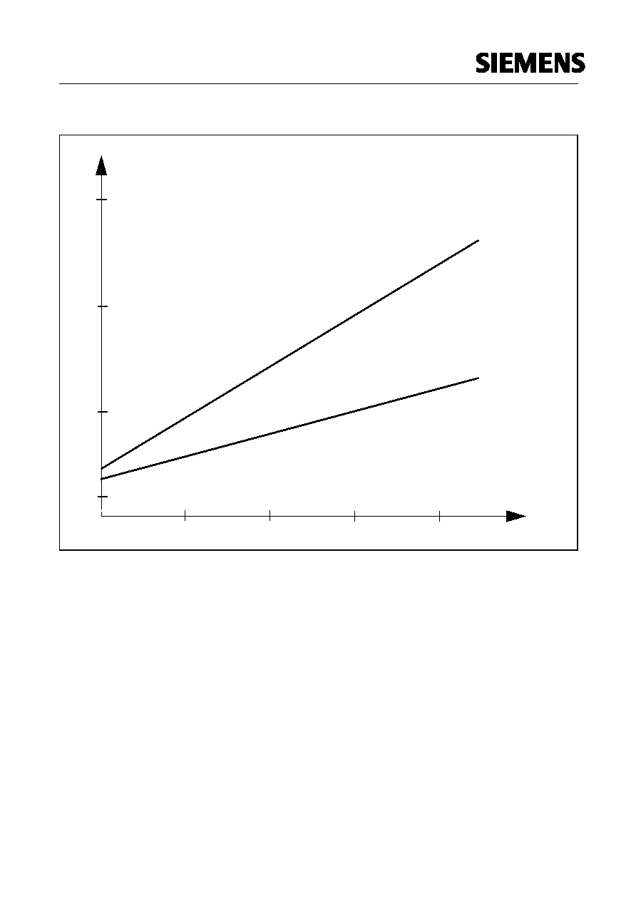
20Dec96@09:25h Intermediate Version
Semiconductor Group
40
C167CR-16RM
Figure 8
Supply/Idle Current as a Function of Operating Frequency
AA
AA
AA
AAAA
AAAA
AAAA
AAAA
AAAA
AAAA
AAAA
AAAA
AAAA
AAAA
AAAA
AAAA
AAAA
AAAA
AAAA
AAAA
AAAA
AAAA
AAAA
AAAA
AAAA
AAAA
AAAA
AAAA
AAAA
AAAA
AAAA
AAAA
AAAA
AAAA
AAAA
AAAA
AAAA
AAAA
AAAA
AAAA
AAAA
AAAA
AAAA
AAAA
AAAA
AAAA
AAAA
AAAA
AAAA
AAAA
AAAA
AAAA
AAAA
AAAA
AAAA
AAAA
AAAA
AAAA
AAAA
AAAA
AAAA
AAAA
AAAA
AAAA
AAAA
AAAA
AAAA
AAAA
AAAA
AAAA
AAAA
AAAA
AAAA
AAAA
AAAA
AAAA
AAAA
AAAA
AAAA
AAAA
AAAA
AAAA
AAAA
AAAA
AAAA
AAAA
AAAA
AAAA
AAAA
AAAA
AAAA
AAAA
AAAA
AAAA
AAAA
AAAA
AAAA
AAAA
AAAA
AAAA
AAAA
AAAA
AAAA
AAAA
AAAA
AAAA
AAAA
AAAA
AAAA
AAAA
AAAA
AAAA
AAAA
AAAA
AAAA
AAAA
AAAA
AAAA
AAAA
AAAA
AAAA
AAAA
AAAA
AAAA
AAAA
AAAA
AAAA
AAAA
AAAA
AAAA
AAAA
AAAA
AAAA
AAAA
AAAA
AAAA
AAAA
AAAA
AAAA
AAAA
AAAA
AAAA
AAAA
AAAA
AAAA
AAAA
AAAA
AAAA
AAAA
AAAA
AAAA
AAAA
AAAA
AAAA
AAAA
AAAA
AAAA
AAAA
AAAA
AAAA
AAAA
AAAA
AAAA
AAAA
AAAA
AAAA
AAAA
AAAA
AAAA
AAAA
AAAA
AAAA
AAAA
AAAA
AAAA
AAAA
AAAA
AAAA
AAAA
AAAA
AAAA
AAAA
AAAA
AAAA
AAAA
AAAA
AAAA
AAAA
AAAA
AAAA
AAAA
AAAA
AAAA
AAAA
AAAA
AAAA
AAAA
AAAA
AAAA
AAAA
AAAA
AAAA
AAAA
AAAA
AAAA
AAAA
AAAA
AAAA
AAAA
AAAA
AAAA
AAAA
AAAA
AAAA
AAAA
AAAA
AAAA
AAAA
AAAA
AAAA
AAAA
AAAA
AAAA
AAAA
AAAA
AAAA
AAAA
AAAA
AAAA
AAAA
AAAA
AAAA
AAAA
AAAA
AAAA
AAAA
AAAA
AAAA
AAAA
AAAA
AAAA
AAAA
AAAA
AAAA
AAAA
AAAA
AAAA
AAAA
AAAA
AAAA
AAAA
AAAA
AAAA
AAAA
AAAA
AAAA
AAAA
AAAA
AAAA
AAAA
AAAA
AAAA
AAAA
AAAA
AAAA
AAAA
AAAA
AAAA
AAAA
AAAA
AAAA
AAAA
AAAA
AAAA
AAAA
AAAA
AAAA
AAAA
AAAA
AAAA
AAAA
AAAA
AAAA
AAAA
AAAA
AAAA
AAAA
AAAA
AAAA
AAAA
AAAA
AAAA
AAAA
AAAA
AAAA
AAAA
AAAA
AAAA
AAAA
AAAA
AAAA
AAAA
AAAA
AAAA
AAAA
AAAA
AAAA
AAAA
AAAA
AAAA
AAAA
AAAA
AAAA
AAAA
AAAA
AAAA
AAAA
AAAA
AAAA
AAAA
AAAA
AAAA
AAAA
AAAA
AAAA
AAAA
AAAA
AAAA
AAAA
AAAA
AAAA
AAAA
AAAA
AAAA
AAAA
AAAA
AAAA
AAAA
AAAA
AAAA
AAAA
AAAA
AAAA
AAAA
AAAA
AAAA
AAAA
AAAA
AAAA
AAAA
AAAA
AAAA
AAAA
AAAA
AAAA
AAAA
AAAA
AAAA
AAAA
AAAA
AAAA
AAAA
AAAA
AAAA
AAAA
AAAA
AAAA
AAAA
AAAA
AAAA
AAAA
AAAA
AAAA
AAAA
AAAA
AAAA
AAAA
AAAA
AAAA
AAAA
AAAA
AAAA
AAAA
AAAA
AAAA
AAAA
AAAA
AAAA
AAAA
AAAA
AAAA
AAAA
AAAA
AAAA
AAAA
AAAA
AAAA
AAAA
AAAA
AAAA
AAAA
AAAA
AAAA
AAAA
AAAA
AAAA
AAAA
AAAA
AAAA
AAAA
AAAA
AAAA
AAAA
AAAA
AAAA
AAAA
AAAA
AAAA
AAAA
AAAA
AAAA
AAAA
AAAA
AAAA
AAAA
AAAA
AAAA
AAAA
AAAA
AAAA
AAAA
AAAA
AAAA
AAAA
AAAA
AAAA
AAAA
AAAA
AAAA
AAAA
AAAA
AAAA
AAAA
AAAA
AAAA
AAAA
AAAA
AAAA
AAAA
AAAA
AAAA
AAAA
AAAA
AAAA
AAAA
AAAA
AAAA
AAAA
AAAA
AAAA
AAAA
AAAA
AAAA
AAAA
AAAA
AAAA
AAAA
AAAA
AAAA
AAAA
AAAA
AAAA
AAAA
AAAA
AAAA
AAAA
AAAA
AAAA
AAAA
AAAA
AAAA
AAAA
AAAA
AAAA
AAAA
AAAA
AAAA
AAAA
AAAA
AAAA
AAAA
AAAA
AAAA
AAAA
AAAA
AAAA
AAAA
AAAA
AAAA
AAAA
AAAA
AAAA
AAAA
AAAA
AAAA
AAAA
AAAA
AAAA
AAAA
AAAA
AAAA
AAAA
AAAA
AAAA
AAAA
AAAA
AAAA
AAAA
AAAA
AAAA
AAAA
AAAA
AAAA
AAAA
AAAA
AAAA
AAAA
AAAA
AAAA
AAAA
AAAA
AAAA
AAAA
AAAA
AAAA
AAAA
AAAA
AAAA
AAAA
AAAA
AAAA
AAAA
AAAA
AAAA
AAAA
AAAA
AAAA
AAAA
AAAA
AAAA
AAAA
AAAA
AAAA
AAAA
AAAA
AAAA
AAAA
AAAA
AAAA
AAAA
AAAA
AAAA
AAAA
AAAA
AAAA
AAAA
AAAA
AAAA
AAAA
AAAA
AAAA
AAAA
AAAA
AAAA
AAAA
AAAA
AAAA
AAAA
AAAA
AAAA
AAAA
AAAA
AAAA
AAAA
AAAA
AAAA
AAAA
AAAA
AAAA
AAAA
AAAA
AAAA
AAAA
AAAA
AAAA
AAAA
AAAA
AAAA
AAAA
AAAA
AAAA
AAAA
AAAA
AAAA
AAAA
AAAA
AAAA
AAAA
AAAA
AAAA
AAAA
AAAA
AAAA
AAAA
AAAA
AAAA
AAAA
AAAA
AAAA
AAAA
AAAA
AAAA
AAAA
AAAA
AAAA
AAAA
AAAA
AAAA
AAAA
AAAA
AAAA
AAAA
AAAA
AAAA
AAAA
AAAA
AAAA
AAAA
AAAA
AAAA
AAAA
AAAA
AAAA
AAAA
AAAA
AAAA
AAAA
AAAA
AAAA
AAAA
AAAA
AAAA
AAAA
AAAA
AAAA
AAAA
AAAA
AAAA
AAAA
AAAA
AAAA
AAAA
AAAA
AAAA
AAAA
AAAA
AAAA
AAAA
AAAA
AAAA
AAAA
AAAA
AAAA
AAAA
AAAA
AAAA
AAAA
AAAA
AAAA
AAAA
AAAA
AAAA
AAAA
AAAA
AAAA
AAAA
AAAA
AAAA
AAAA
AAAA
AAAA
AAAA
AAAA
AAAA
AAAA
AAAA
AAAA
AAAA
AAAA
AAAA
AAAA
AAAA
AAAA
AAAA
AAAA
AAAA
AAAA
AAAA
AAAA
AAAA
AAAA
AAAA
AAAA
AAAA
AAAA
AAAA
AAAA
AAAA
AAAA
AAAA
AAAA
AAAA
AAAA
AAAA
AAAA
AAAA
AAAA
AAAA
AAAA
AAAA
AAAA
AAAA
AAAA
AAAA
AAAA
AAAA
AAAA
AAAA
AAAA
AAAA
AAAA
AAAA
AAAA
AAAA
AAAA
AAAA
AAAA
AAAA
AAAA
AAAA
AAAA
AAAA
AAAA
AAAA
AAAA
AAAA
AAAA
AAAA
AAAA
AAAA
AAAA
AAAA
AAAA
AAAA
AAAA
AAAA
AAAA
AAAA
AAAA
AAAA
AAAA
AAAA
AAAA
AAAA
AAAA
AAAA
AAAA
AAAA
AAAA
AAAA
AAAA
AAAA
AAAA
AAAA
AAAA
AAAA
AAAA
AAAA
AAAA
AAAA
AAAA
AAAA
AAAA
AAAA
AAAA
AAAA
AAAA
AAAA
AAAA
AAAA
AAAA
AAAA
AAAA
AAAA
AAAA
AAAA
AAAA
AAAA
AAAA
AAAA
AAAA
AAAA
AAAA
AAAA
AAAA
AAAA
AAAA
AAAA
AAAA
AAAA
AAAA
AAAA
AAAA
AAAA
AAAA
AAAA
AAAA
AAAA
AAAA
AAAA
AAAA
AAAA
AAAA
AAAA
AAAA
AAAA
AAAA
AAAA
AAAA
AAAA
AAAA
AAAA
AAAA
AAAA
AAAA
AAAA
AAAA
AAAA
AAAA
AAAA
AAAA
AAAA
AAAA
AAAA
AAAA
AAAA
AAAA
AAAA
AAAA
AAAA
AAAA
AAAA
AAAA
AAAA
AAAA
AAAA
AAAA
AAAA
AAAA
AAAA
AAAA
AAAA
AAAA
AAAA
AAAA
AAAA
AAAA
AAAA
AAAA
AAAA
AAAA
AAAA
AAAA
AAAA
AAAA
AAAA
AAAA
AAAA
AAAA
AAAA
AAAA
AAAA
AAAA
AAAA
AAAA
AAAA
AAAA
AAAA
AAAA
AAAA
AAAA
AAAA
AAAA
AAAA
AAAA
AAAA
AAAA
AAAA
AAAA
AAAA
AAAA
AAAA
AAAA
AAAA
AAAA
AAAA
AAAA
AAAA
AAAA
AAAA
AAAA
AAAA
AAAA
AAAA
AAAA
AAAA
AAAA
AAAA
AAAA
AAAA
AAAA
AAAA
AAAA
AAAA
AAAA
AAAA
AAAA
AAAA
AAAA
AAAA
AAAA
AAAA
AAAA
AAAA
AAAA
AAAA
AAAA
AAAA
AAAA
AAAA
AAAA
AAAA
AAAA
AAAA
AAAA
AAAA
AAAA
AAAA
AAAA
AAAA
AAAA
AAAA
AAAA
AAAA
AAAA
AAAA
AAAA
AAAA
AAAA
AAAA
AAAA
AAAA
AAAA
AAAA
AAAA
AAAA
AAAA
AAAA
AAAA
AAAA
AAAA
AAAA
AAAA
AAAA
AAAA
AAAA
AAAA
AAAA
AAAA
AAAA
AAAA
AAAA
AAAA
AAAA
AAAA
AAAA
AAAA
AAAA
AAAA
AAAA
AAAA
AAAA
AAAA
AAAA
AAAA
AAAA
AAAA
AAAA
AAAA
AAAA
AAAA
AAAA
AAAA
AAAA
AAAA
AAAA
AAAA
AAAA
AAAA
AAAA
AAAA
AAAA
AAAA
AAAA
AAAA
AAAA
AAAA
AAAA
AAAA
AAAA
AAAA
AAAA
AAAA
AAAA
AAAA
AAAA
AAAA
AAAA
AAAA
AAAA
AAAA
AAAA
AAAA
AAAA
AAAA
AAAA
AAAA
AAAA
AAAA
AAAA
AAAA
AAAA
AAAA
AAAA
AAAA
AAAA
AAAA
AAAA
AAAA
AAAA
AAAA
AAAA
AAAA
AAAA
AAAA
AAAA
AAAA
AAAA
AAAA
AAAA
AAAA
AAAA
AAAA
AAAA
AAAA
AAAA
AAAA
AAAA
AAAA
AAAA
AAAA
AAAA
AAAA
AAAA
AAAA
AAAA
AAAA
AAAA
AAAA
AAAA
AAAA
AAAA
AAAA
AAAA
AAAA
AAAA
AAAA
AAAA
AAAA
AAAA
AAAA
AAAA
AAAA
AAAA
AAAA
AAAA
AAAA
AAAA
AAAA
AAAA
AAAA
AAAA
AAAA
AAAA
AAAA
AAAA
AAAA
AAAA
AAAA
AAAA
AAAA
AAAA
AAAA
AAAA
AAAA
AAAA
AAAA
AAAA
AAAA
AAAA
AAAA
AA
AA
AA
AA
AA
AA
AA
AA
AA
AA
AA
AA
AA
AA
AA
AA
AA
AA
AA
AA
AA
AA
AA
AA
AA
AA
AA
AA
AA
AA
AA
AA
AA
AA
AA
AA
AA
AA
AA
AA
AA
AA
AA
AA
AA
AA
AA
AA
AA
AA
AA
AA
AA
AAAA
AAAA
AAAA
AAAA
AAAA
AAAA
AAAA
AAAA
AAAA
AAAA
AAAA
AAAA
AAAA
AAAA
AAAA
AAAA
AAAA
AAAA
AAAA
AAAA
AAAA
AAAA
AAAA
AAAA
AAAA
AAAA
AAAA
AAAA
AAAA
AAAA
AAAA
AAAA
AAAA
AAAA
AAAA
AAAA
AAAA
AAAA
AAAA
AAAA
AAAA
AAAA
AA
AA
AAAA
AAAA
AAAA
AAAA
AAAA
AAAA
AAAA
AAAA
AAAA
AAAA
AAAA
AAAA
AAAA
AAAA
AAAA
AAAA
AAAA
AAAA
AAAA
AAAA
AAAA
AAAA
AAAA
AAAA
AAAA
AAAA
AAAA
AAAA
AAAA
AAAA
AAAA
AAAA
AAAA
AAAA
AAAA
AAAA
AAAA
AAAA
AAAA
AAAA
AAAA
AAAA
AA
AA
AA
AA
AA
AA
AA
AA
AA
AA
AA
AA
AA
AA
AA
AA
AA
AA
AA
AA
AA
AA
AA
AA
AA
AA
AA
AA
AA
AA
AA
AA
AA
AA
AA
AA
AA
AA
AA
AA
AA
AA
AA
AA
AA
AA
AA
AA
AA
AA
AA
AA
AA
AA
AA
AA
AA
AA
AA
AA
AA
AA
AA
AA
I [m
A
]
f
CPU
[MHz]
5
10
15
20
150
100
50
10
I
CCtyp
I
IDmax
I
CCmax
I
IDtyp
AA
AA
AAAA
AAAA
AAAA
AAAA
AAAA
AAAA
AAAA
AAAA
AAAA
AAAA
AAAA
AAAA
AAAA
AAAA
AAAA
AAAA
AAAA
AAAA
AAAA
AAAA
AAAA
AAAA
AAAA
AAAA
AAAA
AAAA
AAAA
AAAA
AAAA
AAAA
AAAA
AAAA
AAAA
AAAA
AAAA
AAAA
AAAA
AAAA
AAAA
AAAA
AAAA
AAAA
AAAA
AAAA
AAAA
AAAA
AAAA
AAAA
AAAA
AAAA
AAAA
AAAA
AAAA
AAAA
AAAA
AAAA
AAAA
AAAA
AAAA
AAAA
AAAA
AAAA
AAAA
AAAA
AAAA
AAAA
AAAA
AAAA
AAAA
AAAA
AAAA
AAAA
AAAA
AAAA
AAAA
AAAA
AAAA
AAAA
AAAA
AAAA
AAAA
AAAA
AAAA
AAAA
AAAA
AAAA
AAAA
AAAA
AAAA
AAAA
AAAA
AAAA
AAAA
AAAA
AAAA
AAAA
AAAA
AAAA
AAAA
AAAA
AAAA
AAAA
AAAA
AAAA
AAAA
AAAA
AAAA
AAAA
AAAA
AAAA
AAAA
AAAA
AAAA
AAAA
AAAA
AAAA
AAAA
AAAA
AAAA
AAAA
AAAA
AAAA
AAAA
AAAA
AAAA
AAAA
AAAA
AAAA
AAAA
AAAA
AAAA
AAAA
AAAA
AAAA
AAAA
AAAA
AAAA
AAAA
AAAA
AAAA
AAAA
AAAA
AAAA
AAAA
AAAA
AAAA
AAAA
AAAA
AAAA
AAAA
AAAA
AAAA
AAAA
AAAA
AAAA
AAAA
AAAA
AAAA
AAAA
AAAA
AAAA
AAAA
AAAA
AAAA
AAAA
AAAA
AAAA
AAAA
AAAA
AAAA
AAAA
AAAA
AAAA
AAAA
AAAA
AAAA
AAAA
AAAA
AAAA
AAAA
AAAA
AAAA
AAAA
AAAA
AAAA
AAAA
AAAA
AAAA
AAAA
AAAA
AAAA
AAAA
AAAA
AAAA
AAAA
AAAA
AAAA
AAAA
AAAA
AAAA
AAAA
AAAA
AAAA
AAAA
AAAA
AAAA
AAAA
AAAA
AAAA
AAAA
AAAA
AAAA
AAAA
AAAA
AAAA
AAAA
AAAA
AAAA
AAAA
AAAA
AAAA
AAAA
AAAA
AAAA
AAAA
AAAA
AAAA
AAAA
AAAA
AAAA
AAAA
AAAA
AAAA
AAAA
AAAA
AAAA
AAAA
AAAA
AAAA
AAAA
AAAA
AAAA
AAAA
AAAA
AAAA
AAAA
AAAA
AAAA
AAAA
AAAA
AAAA
AAAA
AAAA
AAAA
AAAA
AAAA
AAAA
AAAA
AAAA
AAAA
AAAA
AAAA
AAAA
AAAA
AAAA
AAAA
AAAA
AAAA
AAAA
AAAA
AAAA
AAAA
AAAA
AAAA
AAAA
AAAA
AAAA
AAAA
AAAA
AAAA
AAAA
AAAA
AAAA
AAAA
AAAA
AAAA
AAAA
AAAA
AAAA
AAAA
AAAA
AAAA
AAAA
AAAA
AAAA
AAAA
AAAA
AAAA
AAAA
AAAA
AAAA
AAAA
AAAA
AAAA
AAAA
AAAA
AAAA
AAAA
AAAA
AAAA
AAAA
AAAA
AAAA
AAAA
AAAA
AAAA
AAAA
AAAA
AAAA
AAAA
AAAA
AAAA
AAAA
AAAA
AAAA
AAAA
AAAA
AAAA
AAAA
AAAA
AAAA
AAAA
AAAA
AAAA
AAAA
AAAA
AAAA
AAAA
AAAA
AAAA
AAAA
AAAA
AAAA
AAAA
AAAA
AAAA
AAAA
AAAA
AAAA
AAAA
AAAA
AAAA
AAAA
AAAA
AAAA
AAAA
AAAA
AAAA
AAAA
AAAA
AAAA
AAAA
AAAA
AAAA
AAAA
AAAA
AAAA
AAAA
AAAA
AAAA
AAAA
AAAA
AAAA
AAAA
AAAA
AAAA
AAAA
AAAA
AAAA
AAAA
AAAA
AAAA
AAAA
AAAA
AAAA
AAAA
AAAA
AAAA
AAAA
AAAA
AAAA
AAAA
AAAA
AAAA
AAAA
AAAA
AAAA
AAAA
AAAA
AAAA
AAAA
AAAA
AAAA
AAAA
AAAA
AAAA
AAAA
AAAA
AAAA
AAAA
AAAA
AAAA
AAAA
AAAA
AAAA
AAAA
AAAA
AAAA
AAAA
AAAA
AAAA
AAAA
AAAA
AAAA
AAAA
AAAA
AAAA
AAAA
AAAA
AAAA
AAAA
AAAA
AAAA
AAAA
AAAA
AAAA
AAAA
AAAA
AAAA
AAAA
AAAA
AAAA
AAAA
AAAA
AAAA
AAAA
AAAA
AAAA
AAAA
AAAA
AAAA
AAAA
AAAA
AAAA
AAAA
AAAA
AAAA
AAAA
AAAA
AAAA
AAAA
AAAA
AAAA
AAAA
AAAA
AAAA
AAAA
AAAA
AAAA
AAAA
AAAA
AAAA
AAAA
AAAA
AAAA
AAAA
AAAA
AAAA
AAAA
AAAA
AAAA
AAAA
AAAA
AAAA
AAAA
AAAA
AAAA
AAAA
AAAA
AAAA
AAAA
AAAA
AAAA
AAAA
AAAA
AAAA
AAAA
AAAA
AAAA
AAAA
AAAA
AAAA
AAAA
AAAA
AAAA
AAAA
AAAA
AAAA
AAAA
AAAA
AAAA
AAAA
AAAA
AAAA
AAAA
AAAA
AAAA
AAAA
AAAA
AAAA
AAAA
AAAA
AAAA
AAAA
AAAA
AAAA
AAAA
AAAA
AAAA
AA
AA
AA
AA
AA
AA
AA
AA
AA
AA
AA
AA
AA
AA
AA
AA
AA
AA
AA
AA
AA
AA
AA
20Dec96@09:25h Intermediate Version
41
Semiconductor Group
C167CR-16RM
A/D Converter Characteristics
V
CC
= 5 V
±
10 %;
V
SS
= 0 V
T
A
= 0 to +70 ∞C
for SAB-C167CR-16RM
T
A
= -40 to +85 ∞C
for SAF-C167CR-16RM
T
A
= -40 to +125 ∞C
for SAK-C167CR-16RM
4.0 V
V
AREF
V
CC
+0.1 V ;
V
SS
-0.1 V
V
AGND
V
SS
+0.2 V
Sample time and conversion time of the C167CR-16RM's ADC are programmable. The table below
should be used to calculate the above timings.
Parameter
Symbol
Limit Values
Unit
Test Condition
min.
max.
Analog input voltage range
V
AIN
SR
V
AGND
V
AREF
V
1)
Sample time
t
S
CC ≠
2
t
SC
2) 4)
Conversion time
t
C
CC ≠
14
t
CC
+
t
S
+ 4TCL
3) 4)
Total unadjusted error
TUE CC ≠
±
2
LSB
5)
Internal resistance of reference
voltage source
R
AREF
SR ≠
t
CC
/ 165
- 0.25
k
t
CC
in [ns]
6)
7)
Internal resistance of analog
source
R
ASRC
SR ≠
t
S
/ 330
- 0.25
k
t
S
in [ns]
2)
7)
ADC input capacitance
C
AIN
CC ≠
33
pF
7)
ADCON.15|14
(ADCTC)
Conversion clock
t
CC
ADCON.13|12
(ADSTC)
Sample clock
t
SC
00
TCL * 24
00
t
CC
01
Reserved, do not use
01
t
CC
* 2
10
TCL * 96
10
t
CC
* 4
11
TCL * 48
11
t
CC
* 8

20Dec96@09:25h Intermediate Version
Semiconductor Group
42
C167CR-16RM
Notes
1)
V
AIN
may exceed
V
AGND
or
V
AREF
up to the absolute maximum ratings. However, the conversion result in these
cases will be X000
H
or X3FF
H
, respectively.
2)
During the sample time the input capacitance
C
I
can be charged/discharged by the external source. The
internal resistance of the analog source must allow the capacitance to reach its final voltage level within
t
S
.
After the end of the sample time
t
S
, changes of the analog input voltage have no effect on the conversion result.
Values for the sample clock
t
SC
depend on programming and can be taken from the table above.
3)
This parameter includes the sample time
t
S
, the time for determining the digital result and the time to load the
result register with the conversion result.
Values for the conversion clock
t
CC
depend on programming and can be taken from the table above.
4)
This parameter depends on the ADC control logic. It is not a real maximum value, but rather a fixum.
5)
TUE is tested at
V
AREF
=5.0V,
V
AGND
=0V,
V
CC
=4.9V. It is guaranteed by design characterization for all other
voltages within the defined voltage range.
The specified TUE is guaranteed only if an overload condition (see
I
OV
specification) occurs on maximum 2
not selected analog input pins and the absolute sum of input overload currents on all analog input pins does
not exceed 10 mA.
During the reset calibration sequence the maximum TUE may be
±
4 LSB.
6)
During the conversion the ADC's capacitance must be repeatedly charged or discharged. The internal
resistance of the reference voltage source must allow the capacitance to reach its respective voltage level
within
t
CC
. The maximum internal resistance results from the programmed conversion timing.
7)
Not 100% tested, guaranteed by design characterization.
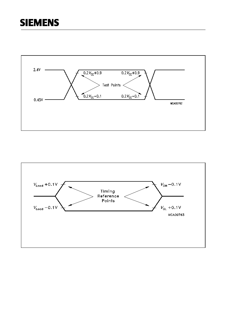
20Dec96@09:25h Intermediate Version
43
Semiconductor Group
C167CR-16RM
Testing Waveforms
Figure 9
Input Output Waveforms
Figure 10
Float Waveforms
AC inputs during testing are driven at 2.4 V for a logic `1' and 0.45 V for a logic `0'.
Timing measurements are made at
V
IH
min for a logic `1' and
V
IL
max for a logic `0'.
For timing purposes a port pin is no longer floating when a 100 mV change from load
voltage occurs, but begins to float when a 100 mV change from the loaded
V
OH
/
V
OL
level occurs
(
I
OH
/
I
OL
= 20 mA).
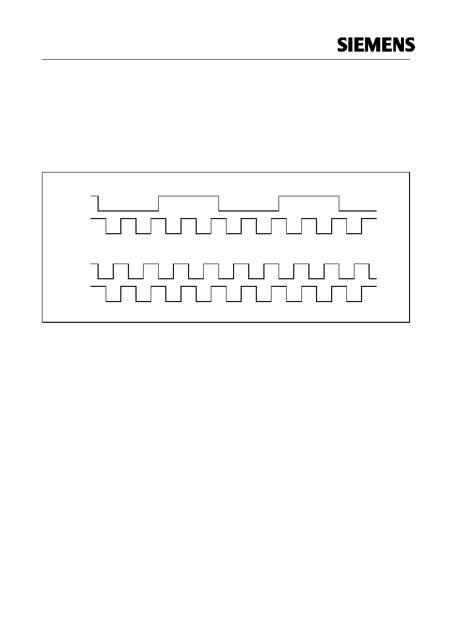
20Dec96@09:25h Intermediate Version
Semiconductor Group
44
C167CR-16RM
AC Characteristics
Definition of Internal Timing
The internal operation of the C167CR-16RM is controlled by the internal CPU clock f
CPU
. Both
edges of the CPU clock can trigger internal (eg. pipeline) or external (eg. bus cycles) operations.
The specification of the external timing (AC Characteristics) therefore depends on the time between
two consecutive edges of the CPU clock, called "TCL" (see figure below).
Figure 11
Generation Mechanisms for the CPU Clock
The CPU clock signal can be generated via different mechanisms. The duration of TCLs and their
variation (and also the derived external timing) depends on the used mechanism to generate f
CPU
.
This influence must be regarded when calculating the timings for the C167CR-16RM.
Direct Drive
When pin P0.15 (P0H.7) is low (`0') during reset the on-chip phase locked loop is disabled and the
CPU clock is directly driven from the internal oscillator with the input clock signal.
The frequency of f
CPU
directly follows the frequency of f
XTAL
so the high and low time of f
CPU
(ie. the
duration of an individual TCL) is defined by the duty cycle of the input clock f
XTAL
.
The timings listed below that refer to TCLs therefore must be calculated using the minimum TCL
that is possible under the respective circumstances. This minimum value can be calculated via the
following formula:
TCL
min
= 1/f
XTAL
* DC
min
(DC = duty cycle)
For two consecutive TCLs the deviation caused by the duty cycle of f
XTAL
is compensated so the
duration of 2TCL is always 1/f
XTAL
. The minimum value TCL
min
therefore has to be used only once
for timings that require an odd number of TCLs (1,3,...). Timings that require an even number of
TCLs (2,4,...) may use the formula 2TCL = 1/f
XTAL
.
Note: The address float timings in Multiplexed bus mode (t
11
and t
45
) use the maximum duration of
TCL (TCL
max
= 1/f
XTAL
* DC
max
) instead of TCL
min
.
A
A
A
A
A
A
A
A
A
A
A
A
A
A
A
TCL TCL
A
A
A
A
A
A
A
A
A
A
A
A
A
A
A
A
A
A
TCL TCL
f
CPU
f
XTAL
f
CPU
f
XTAL
Phase Locked Loop Operation
Direct Clock Drive
20Dec96@09:25h Intermediate Version
45
Semiconductor Group
C167CR-16RM
Phase Locked Loop
When pin P0.15 (P0H.7) is high (`1') during reset the on-chip phase locked loop is enabled and
provides the CPU clock. The PLL multiplies the input frequency by 4 (ie. f
CPU
= f
XTAL
* 4). With every
fourth transition of f
XTAL
the PLL circuit synchronizes the CPU clock to the input clock. This
synchronization is done smoothely, ie. the CPU clock frequency does not change abruptly.
Due to this adaptation to the input clock the frequency of f
CPU
is constantly adjusted so it is locked
to f
XTAL
. The slight variation causes a jitter of f
CPU
which also effects the duration of individual TCLs.
The timings listed in the AC Characteristics that refer to TCLs therefore must be calculated using the
minimum TCL that is possible under the respective circumstances.
The actual minimum value for TCL depends on the jitter of the PLL. As the PLL is constantly
adjusting its output frequency so it corresponds to the applied input frequency (crystal or oscillator)
the relative deviation for periods of more than one TCL is lower than for one single TCL (see formula
and figure below).
For a period of
N * TCL the minimum value is computed using the corresponding deviation D
N
:
TCL
min
= TCL
NOM
* (1 - D
N
/ 100)
D
N
=
±
(4 -
N /15) [%],
where
N = number of consecutive TCLs
and 1
N
40.
So for a period of 3 TCLs (ie.
N = 3): D
3
= 4 -
3/15 = 3.8%,
and TCL
min
= TCL
NOM
* (1 - 3.8 / 100) = TCL
NOM
* 0.962 (24.1 nsec @ f
CPU
= 20 MHz).
This is especially important for bus cycles using waitstates and eg. for the operation of timers, serial
interfaces, etc. For all slower operations and longer periods (eg. pulse train generation or
measurement, lower baudrates, etc.) the deviation caused by the PLL jitter is neglectible.
Figure 12
Approximated Maximum PLL Jitter
32
16
8
4
2
±
1
±
2
±
3
±
4
Max.jitter [%]
N
This approximated formula is valid for
1
N
40 and 10MHz
f
CPU
20MHz.

20Dec96@09:25h Intermediate Version
Semiconductor Group
46
C167CR-16RM
AC Characteristics
External Clock Drive XTAL1
V
CC
= 5 V
±
10 %;
V
SS
= 0 V
T
A
= 0 to +70 ∞C
for SAB-C167CR-16RM
T
A
= -40 to +85 ∞C
for SAF-C167CR-16RM-
T
A
= -40 to +125 ∞C
for SAK-C167CR-16RM
1)
For temperatures above
T
A
= +85 ∞C the minimum value for
t
1
and
t
2
is 25 ns.
2)
The clock input signal must reach the defined levels
V
IL
and
V
IH2
.
Figure 13
External Clock Drive XTAL1
Parameter
Symbol
Direct Drive 1:1
PLL 1:4
Unit
min.
max.
min.
max.
Oscillator period
t
OSC
SR
50
1000
200
333
ns
High time
t
1
SR
23
1)
2)
≠
10
≠
ns
Low time
t
2
SR
23
1)
2)
≠
10
≠
ns
Rise time
t
3
SR
≠
10
2)
≠
10
2)
ns
Fall time
t
4
SR
≠
10
2)
≠
10
2)
ns
20Dec96@09:25h Intermediate Version
47
Semiconductor Group
C167CR-16RM
Memory Cycle Variables
The timing tables below use three variables which are derived from the BUSCONx registers and
represent the special characteristics of the programmed memory cycle. The following table
describes, how these variables are to be computed.
AC Characteristics
Multiplexed Bus
V
CC
= 5 V
±
10 %;
V
SS
= 0 V
T
A
= 0 to +70 ∞C
for SAB-C167CR-16RM
T
A
= -40 to +85 ∞C
for SAF-C167CR-16RM
T
A
= -40 to +125 ∞C
for SAK-C167CR-16RM
C
L
(for PORT0, PORT1, Port 4, ALE, RD, WR, BHE, CLKOUT) = 100 pF
C
L
(for Port 6, CS) = 100 pF
ALE cycle time = 6 TCL + 2
t
A
+
t
C
+
t
F
(150 ns at 20-MHz CPU clock without waitstates)
Description
Symbol Values
ALE Extension
t
A
TCL * <ALECTL>
Memory Cycle Time Waitstates
t
C
2TCL * (15 - <MCTC>)
Memory Tristate Time
t
F
2TCL * (1 - <MTTC>)
Parameter
Symbol
Max. CPU Clock
= 20 MHz
Variable CPU Clock
1/2TCL = 1 to 20 MHz
Unit
min.
max.
min.
max.
ALE high time
t
5
CC
15 +
t
A
≠
TCL - 10 +
t
A
≠
ns
Address setup to ALE
t
6
CC
10 +
t
A
≠
TCL - 15 +
t
A
≠
ns
Address hold after ALE
t
7
CC
15 +
t
A
≠
TCL - 10 +
t
A
≠
ns
ALE falling edge to RD,
WR (with RW-delay)
t
8
CC
15 +
t
A
≠
TCL - 10 +
t
A
≠
ns
ALE falling edge to RD,
WR (no RW-delay)
t
9
CC
-10 +
t
A
≠
-10 +
t
A
≠
ns
Address float after RD,
WR (with RW-delay)
t
10
CC
≠
5
≠
5
ns
Address float after RD,
WR (no RW-delay)
t
11
CC
≠
30
≠
TCL + 5
ns
RD, WR low time
(with RW-delay)
t
12
CC
40 +
t
C
≠
2TCL - 10
+
t
C
≠
ns
RD, WR low time
(no RW-delay)
t
13
CC
65 +
t
C
≠
3TCL - 10
+
t
C
≠
ns
20Dec96@09:25h Intermediate Version
Semiconductor Group
48
C167CR-16RM
RD to valid data in
(with RW-delay)
t
14
SR
≠
30 +
t
C
≠
2TCL - 20
+
t
C
ns
RD to valid data in
(no RW-delay)
t
15
SR
≠
55 +
t
C
≠
3TCL - 20
+
t
C
ns
ALE low to valid data in
t
16
SR
≠
55
+
t
A
+
t
C
≠
3TCL - 20
+
t
A
+
t
C
ns
Address to valid data in
t
17
SR
≠
70
+
2
t
A
+
t
C
≠
4TCL - 30
+
2
t
A
+
t
C
ns
Data hold after RD
rising edge
t
18
SR
0
≠
0
≠
ns
Data float after RD
t
19
SR
≠
35 +
t
F
≠
2TCL - 15
+
t
F
ns
Data valid to WR
t
22
CC
25 +
t
C
≠
2TCL - 25
+
t
C
≠
ns
Data hold after WR
t
23
CC
35 +
t
F
≠
2TCL - 15
+
t
F
≠
ns
ALE rising edge after RD,
WR
t
25
CC
35 +
t
F
≠
2TCL - 15
+
t
F
≠
ns
Address hold after RD,
WR
t
27
CC
35 +
t
F
≠
2TCL - 15
+
t
F
≠
ns
ALE falling edge to CS
t
38
CC
-5 -
t
A
10 -
t
A
-5 -
t
A
10 -
t
A
ns
CS low to Valid Data In
t
39
SR
≠
55
+
t
C
+
2
t
A
≠
3TCL - 20
+
t
C
+
2
t
A
ns
CS hold after RD, WR
t
40
CC
60 +
t
F
≠
3TCL - 15
+
t
F
≠
ns
ALE fall. edge to RdCS,
WrCS (with RW delay)
t
42
CC
20 +
t
A
≠
TCL - 5
+
t
A
≠
ns
ALE fall. edge to RdCS,
WrCS (no RW delay)
t
43
CC
-5 +
t
A
≠
-5
+
t
A
≠
ns
Address float after RdCS,
WrCS (with RW delay)
t
44
CC
≠
0
≠
0
ns
Address float after RdCS,
WrCS (no RW delay)
t
45
CC
≠
25
≠
TCL
ns
RdCS to Valid Data In
(with RW delay)
t
46
SR
≠
25 +
t
C
≠
2TCL - 25
+
t
C
ns
Parameter
Symbol
Max. CPU Clock
= 20 MHz
Variable CPU Clock
1/2TCL = 1 to 20 MHz
Unit
min.
max.
min.
max.
20Dec96@09:25h Intermediate Version
49
Semiconductor Group
C167CR-16RM
RdCS to Valid Data In
(no RW delay)
t
47
SR
≠
50 +
t
C
≠
3TCL - 25
+
t
C
ns
RdCS, WrCS Low Time
(with RW delay)
t
48
CC
40 +
t
C
≠
2TCL - 10
+
t
C
≠
ns
RdCS, WrCS Low Time
(no RW delay)
t
49
CC
65 +
t
C
≠
3TCL - 10
+
t
C
≠
ns
Data valid to WrCS
t
50
CC
35 +
t
C
≠
2TCL - 15
+
t
C
≠
ns
Data hold after RdCS
t
51
SR
0
≠
0
≠
ns
Data float after RdCS
t
52
SR
≠
30 +
t
F
≠
2TCL - 20
+
t
F
ns
Address hold after
RdCS, WrCS
t
54
CC
30 +
t
F
≠
2TCL - 20
+
t
F
≠
ns
Data hold after WrCS
t
56
CC
30 +
t
F
≠
2TCL - 20
+
t
F
≠
ns
Parameter
Symbol
Max. CPU Clock
= 20 MHz
Variable CPU Clock
1/2TCL = 1 to 20 MHz
Unit
min.
max.
min.
max.

20Dec96@09:25h Intermediate Version
Semiconductor Group
50
C167CR-16RM
Figure 14-1
External Memory Cycle: Multiplexed Bus, With Read/Write Delay, Normal ALE
Data In
Data Out
A
A
A
A
A
A
A
A
A
A
A
A
A
A
A
A
A
A
A
A
A
A
A
A
A
A
A
A
A
A
A
A
A
A
A
A
A
A
A
A
A
A
A
A
A
A
A
A
A
A
A
A
A
A
A
A
A
A
A
A
A
A
A
A
A
A
A
A
A
A
A
A
A
A
A
A
A
A
A
A
A
A
A
A
A
A
A
A
A
A
A
A
A
A
A
A
A
A
A
A
A
A
A
A
A
A
A
A
A
A
A
A
A
A
A
A
A
A
A
A
A
A
A
A
A
A
A
A
A
A
A
A
A
A
A
A
A
A
A
A
A
A
A
A
A
A
AA
AA
AA
AA
AA
AA
AA
AA
AA
AA
AA
AA
AA
AA
AA
AA
AA
AA
AA
AA
AA
AA
AA
AA
AA
AA
AA
AA
AA
AA
AA
AA
AA
A
A
A
A
A
A
A
A
A
A
A
A
A
A
A
A
A
A
A
A
A
A
A
A
A
A
A
A
A
A
A
A
A
A
A
AA
AA
AA
AA
AA
AA
AA
AA
AA
AA
A
A
AA
AA
AA
AA
AA
AA
AA
AA
AA
AA
AA
AA
AA
AA
AA
A
AA
AA
AA
AA
AA
AA
AA
AA
AA
AA
AA
AA
AA
AA
AA
AA
AA
AA
AA
AA
AA
AA
AA
AA
AA
AA
AA
AA
AA
AA
AA
AA
AA
AA
AA
AA
AA
AA
AA
AA
AA
AA
AA
AA
AA
AA
AA
AA
AA
AA
AA
AA
AA
AA
AA
AA
AA
AA
AA
AA
AA
AA
AA
AA
AA
AA
AA
AA
AA
AA
AA
AA
AA
AA
AA
AA
AA
AA
AA
AA
AA
AA
A
A
A
A
A
A
A
A
A
A
A
A
Address
Address
t
38
t
44
t
10
A
A
A
A
A
A
A
A
A
A
A
A
A
A
A
A
A
A
AA
AA
AA
AA
AA
AA
AA
AA
AA
AA
AA
AA
AA
AA
AA
AA
AA
A
AA
AA
AA
AA
AA
AA
AA
AA
AA
AA
AA
AA
AA
AA
AA
A
AA
AA
AA
AA
AA
AA
AA
AA
AA
AA
AA
AA
AA
AA
AA
AA
AA
AA
AA
AA
AA
AA
AA
AA
AA
AA
AA
AA
AA
AA
AA
AA
AA
AA
AA
A
A
A
A
A
A
A
A
A
A
A
A
A
A
A
A
A
A
A
A
A
A
A
A
A
A
A
A
A
A
A
A
A
A
A
A
A
A
A
A
A
A
A
A
A
A
A
A
A
A
A
A
A
A
A
A
A
A
A
A
A
A
A
A
A
A
A
A
A
A
A
A
A
A
AA
AA
AA
AA
AA
AA
AA
AA
AA
AA
AA
AA
AA
AA
AA
AA
AA
AA
AA
AA
AA
AA
AA
AA
AA
AA
AA
AA
AA
AA
AA
AA
AA
A
A
A
A
A
A
A
A
A
A
A
A
A
A
A
A
A
A
A
A
A
A
A
A
A
A
A
A
A
A
A
A
A
A
A
A
A
A
A
A
A
A
A
A
A
A
A
A
A
A
A
A
A
A
A
A
A
A
A
A
A
A
A
A
A
A
A
A
A
A
A
A
A
A
A
A
A
A
A
A
A
A
A
A
A
A
A
A
A
A
A
A
A
A
A
A
A
A
A
A
A
A
A
A
A
A
A
A
A
A
A
A
A
A
A
A
AA
AA
AA
AA
AA
AA
AA
AA
AA
AA
AA
AA
AA
AA
AA
AA
AA
AA
AA
AA
AA
AA
AA
AA
AA
AA
AA
AA
AA
AA
AA
AA
AA
AA
AA
AA
AA
AA
AA
AA
AA
AA
AA
AA
AA
AA
AA
AA
AA
AA
AA
AA
AA
AA
AA
AA
AA
AA
AA
AA
AA
AA
AA
AA
AA
AA
AA
AA
AA
AA
AA
AA
AA
AA
AA
AA
AA
AA
AA
AA
AA
AA
AA
A
AA
AA
AA
AA
AA
AA
AA
AA
AA
AA
AA
AA
AA
AA
AA
AA
AA
AA
AA
AA
AA
AA
AA
AA
AA
AA
AA
AA
AA
AA
AA
AA
AA
AA
AA
AA
AA
AA
AA
AA
AA
AA
AA
AA
AA
AA
AA
AA
AA
AA
AA
AA
AA
AA
AA
AA
AA
AA
AA
AA
AA
AA
AA
AA
AA
AA
AA
AA
AA
AA
AA
AA
AA
AA
AA
AA
AA
AA
AA
AA
AA
AA
AA
AA
AA
AA
AA
AA
AA
A
A
A
A
A
A
A
A
A
A
A
A
A
AA
A
AA
AA
AA
AA
AA
AA
AA
AA
AA
AA
AA
AA
AA
AA
AA
AA
AA
AA
AA
AA
AA
AA
AA
AA
AA
AA
AA
AA
AA
AA
AA
AA
AA
AA
AA
AA
AA
AA
AA
AA
AA
AA
AA
AA
AA
AA
AA
AA
AA
AA
AA
AA
AA
AA
AA
AA
AA
AA
AA
AA
AA
AA
AA
AA
AA
AA
AA
AA
AA
AA
AA
AA
AA
AA
AA
AA
AA
AA
AA
AA
AA
AA
AA
AA
AA
AA
AA
AA
AA
AA
AA
AA
AA
AA
AA
AA
AA
AA
AA
AA
AA
AA
AA
AA
AA
AA
AA
AA
AA
AA
AA
AA
AA
AA
AA
AA
AA
AA
AA
AA
AA
AA
AA
AA
AA
AA
AA
AA
AA
AA
AA
AA
AA
AA
AA
AA
AA
AA
Address
ALE
CSx
A23-A16
(A15-A8)
BHE
BUS
Read Cycle
RD
RdCSx
BUS
Write Cycle
WR,
WRL, WRH
WrCSx
t
5
t
16
t
17
t
6
t
7
t
39
t
40
t
25
t
27
t
18
t
19
t
14
t
46
t
12
t
48
t
10
t
22
t
23
t
44
t
12
t
48
t
8
t
42
t
42
t
8
t
50
t
51
t
54
t
52
t
56
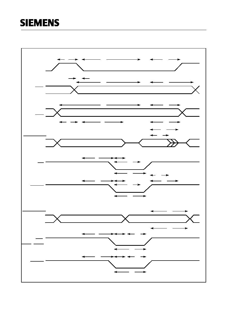
20Dec96@09:25h Intermediate Version
51
Semiconductor Group
C167CR-16RM
Figure 14-2
External Memory Cycle: Multiplexed Bus, With Read/Write Delay, Extended ALE
A
A
A
A
A
A
A
A
A
A
A
A
A
A
A
A
A
A
A
A
A
A
A
A
A
A
A
A
A
A
A
A
A
AA
AA
AA
AA
AA
AA
AA
AA
AA
AA
AA
AA
AA
AA
AA
AA
AA
AA
AA
AA
AA
AA
AA
AA
AA
AA
AA
AA
AA
AA
AA
AA
AA
AA
AA
AA
AA
AA
AA
AA
AA
AA
AA
AA
AA
AA
AA
AA
AA
AA
A
AA
AA
AA
AA
AA
AA
AA
AA
AA
AA
AA
AA
AA
AA
AA
AA
AA
AA
AA
AA
AA
AA
AA
AA
AA
AA
AA
AA
AA
AA
AA
AA
AA
AA
AA
AA
AA
AA
AA
AA
AA
AA
AA
AA
AA
AA
AA
AA
AA
AA
AA
AA
AA
AA
AA
AA
AA
AA
AA
AA
AA
AA
AA
AA
AA
AA
AA
AA
AA
AA
AA
AA
AA
AA
AA
AA
AA
AA
AA
AA
AA
AA
A
A
A
A
A
A
A
A
A
A
A
A
Data Out
Address
Data In
Address
t
38
t
44
t
10
A
A
A
A
A
A
A
A
A
A
A
A
A
A
A
A
A
A
AA
AA
AA
AA
AA
AA
AA
AA
AA
AA
AA
AA
AA
AA
AA
AA
AA
AA
AA
AA
AA
AA
AA
AA
AA
AA
AA
AA
AA
AA
AA
AA
AA
AA
AA
AA
AA
AA
AA
AA
AA
AA
AA
AA
AA
AA
AA
AA
AA
AA
AA
AA
AA
AA
AA
AA
AA
AA
AA
AA
AA
AA
AA
AA
AA
A
A
A
A
A
A
A
A
A
A
A
A
A
A
A
A
A
A
A
A
A
A
A
A
A
A
A
A
A
A
A
A
A
A
A
A
A
A
A
A
A
A
A
A
A
A
A
A
A
A
A
A
A
A
A
A
A
A
A
A
A
A
A
A
A
A
A
A
A
A
A
A
A
A
AA
AA
AA
AA
AA
AA
AA
AA
AA
AA
AA
AA
AA
AA
AA
AA
AA
AA
AA
AA
AA
AA
AA
AA
AA
AA
AA
AA
AA
AA
AA
AA
AA
AA
AA
AA
AA
AA
AA
AA
AA
AA
AA
AA
AA
AA
AA
AA
AA
AA
AA
AA
AA
AA
AA
AA
AA
AA
AA
AA
AA
AA
AA
AA
AA
AA
AA
AA
AA
AA
AA
AA
AA
AA
AA
AA
AA
AA
AA
A
A
A
A
A
A
A
A
A
A
A
A
A
A
A
A
A
A
A
A
A
A
A
A
A
A
A
A
A
A
A
A
A
A
A
A
A
A
A
A
A
A
A
A
A
A
A
A
A
A
A
A
A
A
A
A
A
A
A
A
A
A
A
A
A
A
A
A
A
A
A
A
A
A
A
A
A
A
A
A
AA
AA
AA
AA
AA
AA
AA
AA
AA
AA
AA
AA
AA
AA
AA
AA
AA
AA
AA
AA
AA
AA
AA
AA
AA
AA
AA
AA
AA
AA
AA
AA
AA
AA
AA
AA
AA
AA
AA
AA
A
A
A
A
A
A
A
A
A
A
A
A
A
A
A
A
A
A
A
A
A
A
A
A
A
A
A
A
A
A
A
A
A
A
A
A
A
A
A
A
A
A
AA
A
AA
AA
AA
AA
AA
AA
AA
AA
AA
AA
AA
AA
AA
AA
AA
AA
AA
AA
AA
AA
AA
AA
AA
AA
AA
AA
AA
AA
AA
AA
AA
AA
AA
AA
AA
AA
AA
AA
AA
AA
AA
AA
AA
AA
AA
AA
AA
AA
AA
AA
AA
AA
AA
AA
AA
AA
AA
AA
AA
AA
AA
AA
AA
AA
AA
AA
AA
AA
AA
AA
AA
AA
AA
AA
AA
AA
AA
AA
AA
AA
AA
AA
AA
AA
AA
AA
AA
AA
AA
AA
AA
AA
AA
AA
AA
AA
AA
AA
AA
AA
AA
AA
AA
AA
AA
AA
AA
AA
AA
AA
AA
AA
AA
AA
AA
AA
AA
AA
AA
AA
AA
AA
AA
AA
AA
AA
AA
AA
AA
AA
AA
AA
AA
AA
AA
AA
AA
AA
AA
AA
AA
AA
AA
AA
A
A
A
A
A
A
A
A
A
A
A
A
A
A
A
A
A
A
A
A
A
A
A
A
A
A
A
A
A
A
A
A
A
A
A
A
A
A
A
A
A
A
A
A
A
A
A
A
A
A
A
A
A
A
A
A
A
A
A
A
A
A
A
A
A
A
A
A
A
A
A
A
A
A
A
A
A
A
A
A
A
A
A
A
A
A
A
A
A
A
A
A
A
A
A
A
A
A
A
A
A
A
A
A
A
A
AA
A
AA
AA
AA
AA
AA
AA
AA
AA
AA
AA
AA
AA
AA
AA
AA
AA
AA
AA
AA
AA
AA
AA
AA
AA
AA
AA
AA
AA
AA
AA
AA
AA
AA
AA
AA
AA
AA
AA
AA
AA
AA
AA
AA
AA
AA
AA
AA
AA
AA
AA
AA
AA
AA
AA
AA
AA
AA
AA
AA
AA
AA
AA
AA
AA
AA
AA
AA
AA
AA
AA
AA
AA
AA
AA
AA
AA
AA
AA
AA
AA
AA
AA
AA
AA
AA
AA
AA
AA
AA
AA
AA
AA
AA
AA
AA
AA
AA
AA
AA
AA
AA
AA
AA
AA
AA
AA
AA
AA
AA
AA
AA
AA
AA
AA
AA
AA
AA
AA
AA
AA
AA
AA
AA
AA
AA
AA
AA
AA
AA
AA
AA
AA
AA
AA
AA
AA
AA
AA
Address
ALE
CSx
A23-A16
(A15-A8)
BHE
BUS
Read Cycle
RD
RdCSx
BUS
Write Cycle
WR,
WRL, WRH
WrCSx
t
5
t
16
t
17
t
6
t
7
t
39
t
40
t
25
t
27
t
18
t
19
t
14
t
46
t
12
t
48
t
10
t
22
t
23
t
44
t
12
t
48
t
8
t
42
t
42
t
8
t
50
t
51
t
54
t
52
t
56
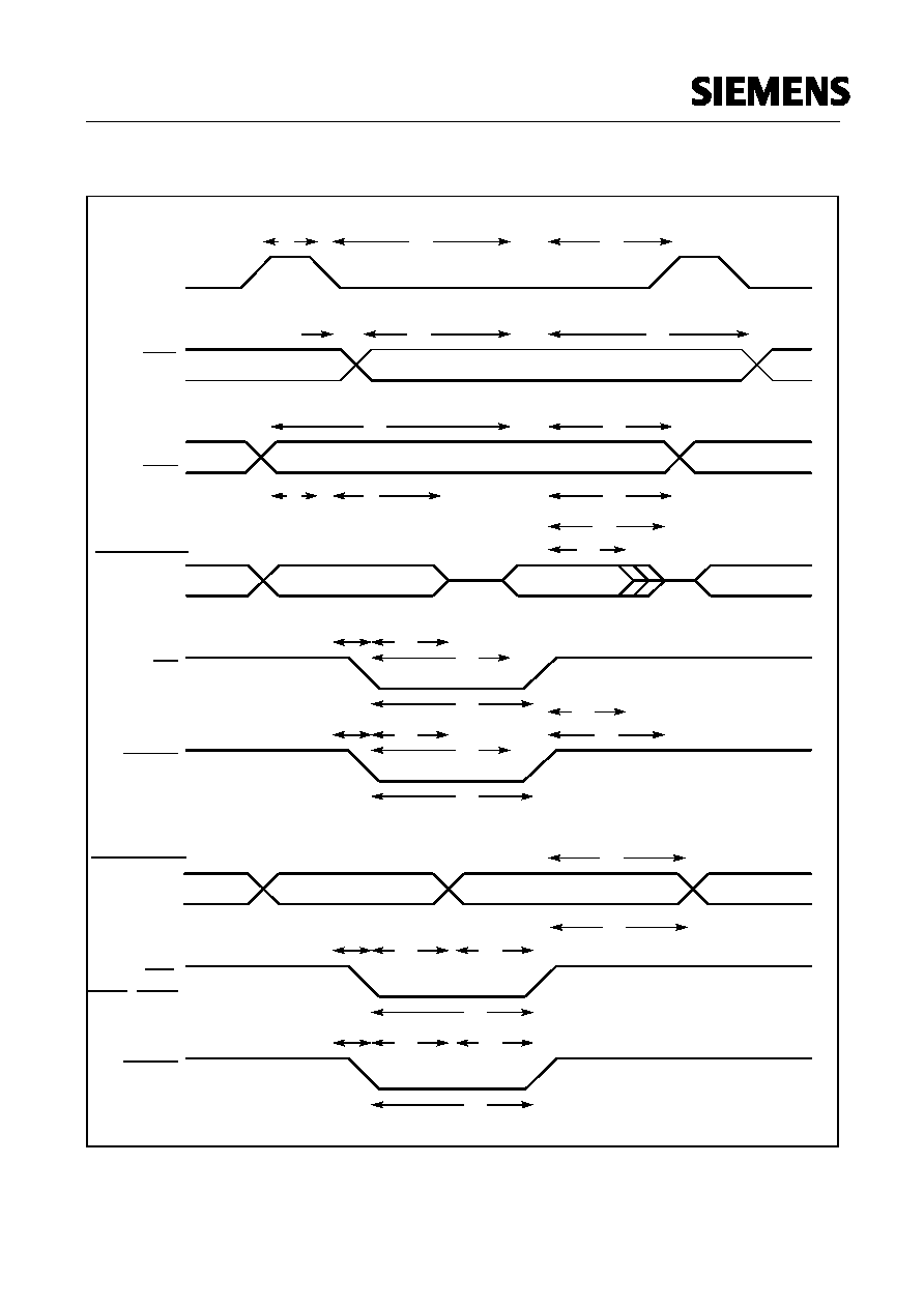
20Dec96@09:25h Intermediate Version
Semiconductor Group
52
C167CR-16RM
Figure 14-3
External Memory Cycle: Multiplexed Bus, No Read/Write Delay, Normal ALE
AA
AA
AA
AA
AA
AA
AA
AA
AA
AA
AA
AA
AA
AA
AA
AA
AA
AA
AA
AA
AA
AA
AA
AA
AA
AA
AA
AA
AA
AA
AA
AA
AA
A
A
A
A
A
A
A
A
A
A
A
A
A
A
A
A
A
A
A
A
A
A
A
A
A
A
A
A
A
A
A
A
A
A
A
A
A
A
A
A
A
A
A
A
A
A
A
A
A
AA
A
AA
AA
AA
AA
AA
AA
AA
AA
AA
AA
AA
AA
AA
AA
AA
AA
AA
AA
AA
AA
AA
AA
AA
AA
AA
AA
AA
AA
AA
AA
AA
AA
AA
AA
AA
AA
AA
AA
AA
AA
AA
AA
AA
AA
AA
AA
AA
AA
AA
AA
AA
AA
AA
AA
AA
AA
AA
AA
AA
AA
AA
AA
AA
AA
AA
AA
AA
AA
AA
AA
AA
AA
AA
AA
AA
AA
AA
AA
AA
AA
AA
AA
A
A
A
A
A
A
A
A
A
A
A
A
Data Out
Address
Address
Data In
t
38
A
A
A
A
A
A
A
A
A
A
A
A
A
A
A
A
A
A
AA
AA
AA
AA
AA
AA
AA
AA
AA
AA
AA
AA
AA
AA
AA
AA
AA
A
AA
AA
AA
AA
AA
AA
AA
AA
AA
AA
AA
AA
AA
AA
A
A
A
A
A
A
A
A
A
A
A
A
A
A
A
A
A
A
A
A
A
A
A
A
A
A
A
A
A
A
A
A
A
A
A
A
A
A
A
A
A
A
A
A
A
A
A
A
A
A
A
A
A
A
A
A
A
A
A
A
A
A
A
A
A
A
A
A
A
A
A
A
A
A
A
A
A
A
A
A
A
A
A
A
A
A
A
A
A
A
A
A
A
A
A
A
A
A
A
A
A
A
A
A
A
A
A
A
A
AA
AA
AA
AA
AA
AA
AA
AA
AA
AA
AA
AA
AA
AA
AA
AA
AA
AA
AA
AA
AA
AA
AA
AA
A
A
A
A
A
A
A
A
A
A
A
A
A
A
A
A
A
A
A
A
A
A
A
A
A
A
A
A
A
A
A
A
A
A
A
A
A
A
A
A
A
A
A
A
A
A
A
A
A
A
A
A
A
A
A
A
A
A
A
A
A
A
A
A
A
A
A
A
A
A
A
A
A
A
A
A
A
A
A
A
A
A
A
A
A
A
A
A
A
A
A
A
A
A
A
A
A
A
A
A
A
A
A
A
A
A
A
A
A
A
A
A
A
A
A
A
A
A
A
A
A
A
A
A
A
A
A
A
A
A
A
A
A
A
AA
AA
AA
AA
AA
AA
AA
AA
AA
AA
AA
AA
AA
AA
AA
AA
AA
AA
AA
AA
AA
AA
AA
AA
AA
AA
AA
AA
AA
AA
AA
AA
AA
AA
AA
AA
AA
AA
AA
AA
AA
AA
AA
AA
AA
AA
AA
AA
AA
AA
AA
AA
AA
AA
AA
AA
AA
AA
AA
AA
AA
AA
AA
AA
AA
AA
AA
AA
AA
AA
AA
AA
AA
AA
AA
AA
AA
AA
AA
AA
AA
AA
AA
AA
AA
A
A
A
A
A
A
A
A
A
A
A
A
A
A
A
A
A
A
A
A
A
A
A
A
A
A
A
A
A
A
A
A
A
A
A
A
A
A
A
A
A
A
A
A
A
A
A
A
A
A
A
A
A
A
A
A
A
A
A
A
A
A
A
A
A
A
A
A
A
A
A
A
A
A
A
A
A
A
A
A
A
A
A
A
A
A
A
A
A
A
A
A
A
A
A
A
A
A
A
A
A
A
A
A
A
A
A
A
A
A
A
A
A
A
A
A
A
A
A
A
A
A
A
A
A
A
A
A
A
A
A
A
A
A
A
A
A
A
A
A
A
A
A
A
A
A
AA
A
AA
AA
AA
AA
AA
AA
AA
AA
AA
AA
AA
AA
AA
AA
AA
AA
AA
AA
AA
AA
AA
AA
AA
AA
AA
AA
AA
AA
AA
AA
AA
AA
AA
AA
AA
AA
AA
AA
AA
AA
AA
AA
AA
AA
AA
AA
AA
AA
AA
AA
AA
AA
AA
AA
AA
AA
AA
AA
AA
AA
AA
AA
AA
AA
AA
AA
AA
AA
AA
AA
AA
AA
AA
AA
AA
AA
AA
AA
AA
AA
AA
AA
AA
AA
AA
AA
AA
AA
AA
A
A
A
A
A
A
A
A
A
A
A
A
A
AA
A
AA
AA
AA
AA
AA
AA
AA
AA
AA
AA
AA
AA
AA
AA
AA
AA
AA
AA
AA
AA
AA
AA
AA
AA
AA
AA
AA
AA
AA
AA
AA
AA
AA
AA
AA
AA
AA
AA
AA
AA
AA
AA
AA
AA
AA
AA
AA
AA
AA
AA
AA
AA
AA
AA
AA
AA
AA
AA
AA
AA
AA
AA
AA
AA
AA
AA
AA
AA
AA
AA
AA
AA
AA
AA
AA
AA
AA
AA
AA
AA
AA
AA
AA
AA
AA
AA
AA
AA
AA
AA
AA
AA
AA
AA
AA
AA
AA
AA
AA
AA
AA
AA
AA
AA
AA
AA
AA
AA
AA
AA
AA
AA
AA
AA
AA
AA
AA
AA
AA
AA
AA
AA
AA
AA
AA
AA
AA
AA
AA
AA
AA
AA
AA
AA
AA
AA
AA
AA
Address
ALE
CSx
A23-A16
(A15-A8)
BHE
BUS
Read Cycle
RD
RdCSx
BUS
Write Cycle
WR,
WRL, WRH
WrCSx
t
5
t
16
t
17
t
6
t
7
t
39
t
40
t
25
t
27
t
18
t
19
t
15
t
47
t
13
t
49
t
22
t
23
t
13
t
49
t
9
t
43
t
43
t
9
t
11
t
45
t
11
t
45
t
50
t
51
t
54
t
52
t
56

20Dec96@09:25h Intermediate Version
53
Semiconductor Group
C167CR-16RM
Figure 14-4
External Memory Cycle: Multiplexed Bus, No Read/Write Delay, Extended ALE
A
A
A
A
A
A
A
A
A
A
A
A
A
A
A
A
A
A
A
A
A
A
A
A
A
A
A
A
A
A
A
A
A
AA
AA
AA
AA
AA
AA
AA
AA
AA
AA
AA
AA
AA
AA
AA
AA
AA
AA
AA
AA
AA
AA
AA
AA
AA
AA
AA
AA
AA
AA
AA
AA
AA
AA
AA
AA
AA
AA
AA
AA
AA
AA
AA
AA
AA
AA
AA
AA
AA
AA
A
AA
AA
AA
AA
AA
AA
AA
AA
AA
AA
AA
AA
AA
AA
AA
AA
AA
AA
AA
AA
AA
AA
AA
AA
AA
AA
AA
AA
AA
AA
AA
AA
AA
AA
AA
AA
AA
AA
AA
AA
AA
AA
AA
AA
AA
AA
AA
AA
AA
AA
AA
AA
AA
AA
AA
AA
AA
AA
AA
AA
AA
AA
AA
AA
AA
AA
AA
AA
AA
AA
AA
AA
AA
AA
AA
AA
AA
AA
AA
AA
AA
AA
A
A
A
A
A
A
A
A
A
A
A
A
Data Out
Address
Data In
Address
t
38
A
A
A
A
A
A
A
A
A
A
A
A
A
A
A
A
A
A
AA
AA
AA
AA
AA
AA
AA
AA
AA
AA
AA
AA
AA
AA
AA
AA
AA
AA
AA
AA
AA
AA
AA
AA
AA
AA
AA
AA
AA
AA
AA
AA
AA
AA
AA
AA
AA
AA
AA
AA
AA
AA
AA
AA
AA
AA
AA
AA
AA
AA
AA
AA
AA
AA
AA
AA
AA
AA
AA
AA
AA
AA
AA
AA
AA
A
A
A
A
A
A
A
A
A
A
A
A
A
A
A
A
A
A
A
A
A
A
A
A
A
A
A
A
A
A
A
A
A
A
A
A
A
A
A
A
A
A
A
A
A
A
A
A
A
A
A
A
A
A
A
A
A
A
A
A
A
A
A
A
A
A
A
A
A
A
A
A
A
A
AA
AA
AA
AA
AA
AA
AA
AA
AA
AA
AA
AA
AA
AA
AA
AA
AA
AA
AA
AA
AA
AA
AA
AA
AA
AA
AA
AA
AA
AA
AA
AA
AA
AA
AA
AA
AA
AA
AA
AA
AA
AA
AA
AA
AA
AA
AA
AA
AA
AA
AA
AA
AA
AA
AA
AA
AA
AA
AA
AA
AA
AA
AA
AA
AA
AA
AA
AA
AA
AA
AA
AA
AA
AA
AA
AA
AA
AA
AA
A
A
A
A
A
A
A
A
A
A
A
A
A
A
A
A
A
A
A
A
A
A
A
A
A
A
A
A
A
A
A
A
A
A
A
A
A
A
A
A
A
A
A
A
A
A
A
A
A
A
A
A
A
A
A
A
A
A
A
A
A
A
A
A
A
A
A
A
A
A
A
A
A
A
A
A
A
A
A
A
AA
AA
AA
AA
AA
AA
AA
AA
AA
AA
AA
AA
AA
AA
AA
AA
AA
AA
AA
AA
AA
AA
AA
AA
AA
AA
AA
AA
AA
AA
AA
AA
AA
AA
AA
AA
AA
AA
AA
AA
A
A
A
A
A
A
A
A
A
A
A
A
A
A
A
A
A
A
A
A
A
A
A
A
A
A
A
A
A
A
A
A
A
A
A
A
A
A
A
A
A
A
AA
A
AA
AA
AA
AA
AA
AA
AA
AA
AA
AA
AA
AA
AA
AA
AA
AA
AA
AA
AA
AA
AA
AA
AA
AA
AA
AA
AA
AA
AA
AA
AA
AA
AA
AA
AA
AA
AA
AA
AA
AA
AA
AA
AA
AA
AA
AA
AA
AA
AA
AA
AA
AA
AA
AA
AA
AA
AA
AA
AA
AA
AA
AA
AA
AA
AA
AA
AA
AA
AA
AA
AA
AA
AA
AA
AA
AA
AA
AA
AA
AA
AA
AA
AA
AA
AA
AA
AA
AA
AA
AA
AA
AA
AA
AA
AA
AA
AA
AA
AA
AA
AA
AA
AA
AA
AA
AA
AA
AA
AA
AA
AA
AA
AA
AA
AA
AA
AA
AA
AA
AA
AA
AA
AA
AA
AA
AA
AA
AA
AA
AA
AA
AA
AA
AA
AA
AA
AA
AA
AA
AA
AA
AA
AA
AA
A
A
A
A
A
A
A
A
A
A
A
A
A
A
A
A
A
A
A
A
A
A
A
A
A
A
A
A
A
A
A
A
A
A
A
A
A
A
A
A
A
A
A
A
A
A
A
A
A
A
A
A
A
A
A
A
A
A
A
A
A
A
A
A
A
A
A
A
A
A
A
A
A
A
A
A
A
A
A
A
A
A
A
A
A
A
A
A
A
A
A
A
A
A
A
A
A
A
A
A
A
A
A
A
A
A
AA
A
AA
AA
AA
AA
AA
AA
AA
AA
AA
AA
AA
AA
AA
AA
AA
AA
AA
AA
AA
AA
AA
AA
AA
AA
AA
AA
AA
AA
AA
AA
AA
AA
AA
AA
AA
AA
AA
AA
AA
AA
AA
AA
AA
AA
AA
AA
AA
AA
AA
AA
AA
AA
AA
AA
AA
AA
AA
AA
AA
AA
AA
AA
AA
AA
AA
AA
AA
AA
AA
AA
AA
AA
AA
AA
AA
AA
AA
AA
AA
AA
AA
AA
AA
AA
AA
AA
AA
AA
AA
AA
AA
AA
AA
AA
AA
AA
AA
AA
AA
AA
AA
AA
AA
AA
AA
AA
AA
AA
AA
AA
AA
AA
AA
AA
AA
AA
AA
AA
AA
AA
AA
AA
AA
AA
AA
AA
AA
AA
AA
AA
AA
AA
AA
AA
AA
AA
AA
AA
Address
ALE
CSx
A23-A16
(A15-A8)
BHE
BUS
Read Cycle
RD
RdCSx
BUS
Write Cycle
WR,
WRL, WRH
WrCSx
t
5
t
16
t
17
t
6
t
7
t
39
t
40
t
25
t
27
t
18
t
19
t
15
t
47
t
13
t
49
t
22
t
23
t
13
t
49
t
9
t
43
t
43
t
9
t
11
t
45
t
11
t
45
t
50
t
51
t
54
t
52
t
56
20Dec96@09:25h Intermediate Version
Semiconductor Group
54
C167CR-16RM
AC Characteristics
Demultiplexed Bus
V
CC
= 5 V
±
10 %;
V
SS
= 0 V
T
A
= 0 to +70 ∞C
for SAB-C167CR-16RM
T
A
= -40 to +85 ∞C
for SAF-C167CR-16RM
T
A
= -40 to +125 ∞C
for SAK-C167CR-16RM
C
L
(for PORT0, PORT1, Port 4, ALE, RD, WR, BHE, CLKOUT) = 100 pF
C
L
(for Port 6, CS) = 100 pF
ALE cycle time = 4 TCL + 2
t
A
+
t
C
+
t
F
(100 ns at 20-MHz CPU clock without waitstates)
Parameter
Symbol
Max. CPU Clock
= 20 MHz
Variable CPU Clock
1/2TCL = 1 to 20 MHz
Unit
min.
max.
min.
max.
ALE high time
t
5
CC
15 +
t
A
≠
TCL - 10 +
t
A
≠
ns
Address setup to ALE
t
6
CC
10 +
t
A
≠
TCL - 15 +
t
A
≠
ns
ALE falling edge to RD,
WR (with RW-delay)
t
8
CC
15 +
t
A
≠
TCL - 10
+
t
A
≠
ns
ALE falling edge to RD,
WR (no RW-delay)
t
9
CC
-10 +
t
A
≠
-10
+
t
A
≠
ns
RD, WR low time
(with RW-delay)
t
12
CC
40 +
t
C
≠
2TCL - 10
+
t
C
≠
ns
RD, WR low time
(no RW-delay)
t
13
CC
65 +
t
C
≠
3TCL - 10
+
t
C
≠
ns
RD to valid data in
(with RW-delay)
t
14
SR
≠
30 +
t
C
≠
2TCL - 20
+
t
C
ns
RD to valid data in
(no RW-delay)
t
15
SR
≠
55 +
t
C
≠
3TCL - 20
+
t
C
ns
ALE low to valid data in
t
16
SR
≠
55
+
t
A
+
t
C
≠
3TCL - 20
+
t
A
+
t
C
ns
Address to valid data in
t
17
SR
≠
70
+
2
t
A
+
t
C
≠
4TCL - 30
+
2
t
A
+
t
C
ns
Data hold after RD
rising edge
t
18
SR
0
≠
0
≠
ns
Data float after RD rising
edge (with RW-delay
1)
)
t
20
SR
≠
35 +
t
F
≠
2TCL - 15
+
2
t
A
+
t
F
1)
ns
Data float after RD rising
edge (no RW-delay
1)
)
t
21
SR
≠
15 +
t
F
≠
TCL - 10
+
2
t
A
+
t
F
1)
ns
Data valid to WR
t
22
CC
25 +
t
C
≠
2TCL - 25
+
t
C
≠
ns
Data hold after WR
t
24
CC
15 +
t
F
≠
TCL - 10 +
t
F
≠
ns

20Dec96@09:25h Intermediate Version
55
Semiconductor Group
C167CR-16RM
1)
RW-delay and
t
A
refer to the next following bus cycle.
ALE rising edge after RD,
WR
t
26
CC
-10 +
t
F
≠
-10
+
t
F
≠
ns
Address hold after RD,
WR
t
28
CC
0 +
t
F
≠
0
+
t
F
≠
ns
ALE falling edge to CS
t
38
CC
-5 -
t
A
10 -
t
A
-5 -
t
A
10 -
t
A
ns
CS low to Valid Data In
t
39
SR
≠
55
+
t
C
+
2
t
A
≠
3TCL - 20
+
t
C
+
2
t
A
ns
CS hold after RD, WR
t
41
CC
10 +
t
F
≠
TCL - 15
+
t
F
≠
ns
ALE falling edge to RdCS,
WrCS (with RW-delay)
t
42
CC
20 +
t
A
≠
TCL - 5
+
t
A
≠
ns
ALE falling edge to RdCS,
WrCS (no RW-delay)
t
43
CC
-5 +
t
A
≠
-5
+
t
A
≠
ns
RdCS to Valid Data In
(with RW-delay)
t
46
SR
≠
25 +
t
C
≠
2TCL - 25
+
t
C
ns
RdCS to Valid Data In
(no RW-delay)
t
47
SR
≠
50 +
t
C
≠
3TCL - 25
+
t
C
ns
RdCS, WrCS Low Time
(with RW-delay)
t
48
CC
40 +
t
C
≠
2TCL - 10
+
t
C
≠
ns
RdCS, WrCS Low Time
(no RW-delay)
t
49
CC
65 +
t
C
≠
3TCL - 10
+
t
C
≠
ns
Data valid to WrCS
t
50
CC
35 +
t
C
≠
2TCL - 15
+
t
C
≠
ns
Data hold after RdCS
t
51
SR
0
≠
0
≠
ns
Data float after RdCS
(with RW-delay)
t
53
SR
≠
30 +
t
F
≠
2TCL - 20
+
t
F
ns
Data float after RdCS
(no RW-delay)
t
68
SR
≠
5 +
t
F
≠
TCL - 20
+
t
F
ns
Address hold after
RdCS, WrCS
t
55
CC
-10 +
t
F
≠
-10
+
t
F
≠
ns
Data hold after WrCS
t
57
CC
10 +
t
F
≠
TCL - 15
+
t
F
≠
ns
Parameter
Symbol
Max. CPU Clock
= 20 MHz
Variable CPU Clock
1/2TCL = 1 to 20 MHz
Unit
min.
max.
min.
max.
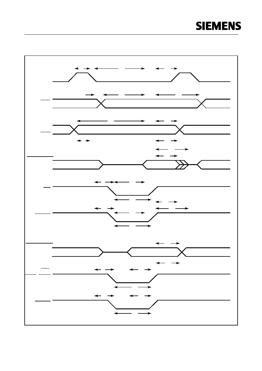
20Dec96@09:25h Intermediate Version
Semiconductor Group
56
C167CR-16RM
Figure 15-1
External Memory Cycle: Demultiplexed Bus, With Read/Write Delay, Normal ALE
AA
AA
AA
AA
AA
AA
AA
AA
AA
AA
AA
AA
AA
AA
AA
AA
AA
AA
AA
AA
AA
AA
AA
AA
AA
AA
AA
AA
AA
AA
AA
AA
AA
A
A
AA
AA
AA
AA
AA
AA
AA
AA
AA
AA
AA
AA
AA
AA
A
A
AA
AA
AA
AA
AA
AA
AA
AA
AA
AA
AA
AA
AA
AA
AA
A
A
A
A
A
A
A
A
A
A
A
A
Data Out
Data In
t
38
AA
AA
AA
AA
AA
AA
AA
AA
AA
AA
AA
AA
AA
AA
AA
AA
AA
AA
AA
AA
AA
AA
AA
AA
AA
AA
AA
AA
AA
AA
AA
AA
AA
AA
AA
A
AA
AA
AA
AA
AA
AA
AA
AA
AA
AA
AA
AA
AA
AA
AA
A
AA
AA
AA
AA
AA
AA
AA
AA
AA
AA
AA
AA
AA
AA
AA
AA
AA
AA
AA
AA
AA
AA
AA
AA
AA
AA
AA
AA
AA
AA
AA
AA
AA
AA
AA
A
A
AA
AA
AA
AA
AA
AA
AA
AA
AA
AA
AA
AA
AA
AA
AA
AA
AA
AA
AA
AA
AA
AA
AA
AA
AA
AA
AA
AA
AA
AA
AA
AA
AA
AA
AA
AA
AA
AA
AA
AA
AA
AA
AA
A
A
A
A
A
A
A
A
A
A
A
A
A
A
A
A
A
A
A
A
A
A
A
A
A
A
A
A
A
A
A
A
A
A
A
A
A
A
A
A
A
A
A
A
A
A
A
A
A
A
A
A
A
A
A
A
A
A
A
A
A
A
A
A
A
A
A
A
A
A
A
A
A
A
A
A
A
A
A
A
A
A
AA
AA
AA
AA
AA
AA
AA
AA
AA
AA
AA
AA
AA
AA
AA
AA
AA
AA
AA
AA
AA
AA
AA
AA
AA
AA
AA
AA
AA
AA
AA
AA
AA
AA
AA
AA
AA
AA
AA
AA
A
A
A
A
A
A
A
A
A
A
A
A
A
A
A
A
A
A
A
A
A
A
A
A
A
A
A
A
A
A
A
A
A
A
A
A
A
A
A
A
A
A
A
A
A
A
A
A
A
A
A
A
A
A
A
A
A
A
A
A
A
A
A
A
A
A
A
A
A
A
A
A
A
A
A
A
A
A
A
A
A
A
A
A
A
A
A
A
A
A
A
A
A
A
A
A
A
A
A
A
A
A
A
A
A
A
A
A
A
A
A
A
A
A
A
A
A
A
A
A
A
A
A
A
A
A
A
A
A
A
A
A
A
A
A
A
A
A
A
A
A
A
A
A
A
A
A
A
A
A
A
A
A
A
A
A
A
A
A
A
A
A
A
A
A
A
A
A
A
A
A
A
A
A
A
A
A
A
A
A
A
A
A
A
A
A
A
A
AA
A
AA
AA
AA
AA
AA
AA
AA
AA
AA
AA
AA
AA
AA
AA
AA
AA
AA
AA
AA
AA
AA
AA
AA
AA
AA
AA
AA
AA
AA
AA
AA
AA
AA
AA
AA
AA
AA
AA
AA
AA
AA
AA
AA
AA
AA
AA
AA
AA
AA
AA
AA
AA
AA
AA
AA
AA
AA
AA
AA
AA
AA
AA
AA
AA
AA
AA
AA
AA
AA
AA
AA
AA
AA
AA
AA
AA
AA
AA
AA
AA
AA
AA
AA
AA
AA
AA
AA
AA
AA
A
A
A
A
A
A
A
A
A
A
A
A
A
AA
A
AA
AA
AA
AA
AA
AA
AA
AA
AA
AA
AA
AA
AA
AA
AA
AA
AA
AA
AA
AA
AA
AA
AA
AA
AA
AA
AA
AA
AA
AA
AA
AA
AA
AA
AA
AA
AA
AA
AA
AA
AA
AA
AA
AA
AA
AA
AA
AA
AA
AA
AA
AA
AA
AA
AA
AA
AA
AA
AA
AA
AA
AA
AA
AA
AA
AA
AA
AA
AA
AA
AA
AA
AA
AA
AA
AA
AA
AA
AA
AA
AA
AA
AA
AA
AA
AA
AA
AA
AA
AA
AA
AA
AA
AA
AA
AA
AA
AA
AA
AA
AA
AA
AA
AA
AA
AA
AA
AA
AA
AA
AA
AA
AA
AA
AA
AA
AA
AA
AA
AA
AA
AA
AA
AA
AA
AA
AA
AA
AA
AA
AA
AA
AA
AA
AA
AA
AA
AA
Address
ALE
CSx
A23-A16
A15-A0
BHE
BUS
(D15-D8)
D7-D0
Read Cycle
RD
RdCSx
Write Cycle
WrCSx
t
5
t
16
t
17
t
6
t
39
t
41
t
26
t
28
t
18
t
20
t
14
t
46
t
12
t
48
t
22
t
24
t
12
t
48
t
8
t
42
t
42
t
8
t
50
t
51
t
55
t
53
t
57
BUS
(D15-D8)
D7-D0
WR,
WRL, WRH

20Dec96@09:25h Intermediate Version
57
Semiconductor Group
C167CR-16RM
Figure 15-2
External Memory Cycle: Demultiplexed Bus, With Read/Write Delay, Extended ALE
A
A
A
A
A
A
A
A
A
A
A
A
A
A
A
A
A
A
A
A
A
A
A
A
A
A
A
A
A
A
A
A
A
AA
AA
AA
AA
AA
AA
AA
AA
AA
AA
AA
AA
AA
AA
AA
AA
A
A
AA
AA
AA
AA
AA
AA
AA
AA
AA
AA
AA
AA
AA
AA
AA
A
A
A
A
A
A
A
A
A
A
A
A
Data Out
Data In
t
38
AA
AA
AA
AA
AA
AA
AA
AA
AA
AA
AA
AA
AA
AA
AA
AA
AA
AA
AA
AA
AA
AA
AA
AA
AA
AA
AA
AA
AA
AA
AA
AA
AA
AA
AA
AA
AA
AA
AA
AA
AA
AA
AA
AA
AA
AA
AA
AA
AA
AA
AA
AA
AA
AA
AA
AA
AA
AA
AA
AA
AA
AA
AA
AA
AA
AA
AA
AA
AA
AA
AA
AA
AA
AA
AA
AA
AA
AA
AA
AA
AA
AA
AA
AA
AA
AA
AA
AA
AA
AA
AA
AA
AA
AA
AA
AA
AA
AA
AA
AA
AA
AA
AA
AA
AA
AA
AA
AA
AA
AA
AA
AA
AA
AA
AA
AA
AA
AA
AA
AA
AA
AA
AA
AA
AA
AA
AA
AA
A
A
A
A
A
A
A
A
A
A
A
A
A
A
A
A
A
A
A
A
A
A
A
A
A
A
A
A
A
A
A
A
A
A
A
A
A
A
A
A
A
A
A
A
A
A
A
A
A
A
A
A
A
A
A
A
A
A
A
A
A
A
A
A
A
A
A
A
A
A
A
A
A
A
A
A
A
A
A
A
AA
AA
AA
AA
AA
AA
AA
AA
AA
AA
AA
AA
AA
AA
AA
AA
AA
AA
AA
AA
AA
AA
AA
AA
AA
AA
AA
AA
AA
AA
AA
AA
AA
AA
AA
AA
AA
AA
AA
AA
A
A
A
A
A
A
A
A
A
A
A
A
A
A
A
A
A
A
A
A
A
A
A
A
A
A
A
A
A
A
A
A
A
A
A
A
A
A
A
A
A
A
AA
A
AA
AA
AA
AA
AA
AA
AA
AA
AA
AA
AA
AA
AA
AA
AA
AA
AA
AA
AA
AA
AA
AA
AA
AA
AA
AA
AA
AA
AA
AA
AA
AA
AA
AA
AA
AA
AA
AA
AA
AA
AA
AA
AA
AA
AA
AA
AA
AA
AA
AA
AA
AA
AA
AA
AA
AA
AA
AA
AA
AA
AA
AA
AA
AA
AA
AA
AA
AA
AA
AA
AA
AA
AA
AA
AA
AA
AA
AA
AA
AA
AA
AA
AA
AA
AA
AA
AA
AA
AA
AA
AA
AA
AA
AA
AA
AA
AA
AA
AA
AA
AA
AA
AA
AA
AA
AA
AA
AA
AA
AA
AA
AA
AA
AA
AA
AA
AA
AA
AA
AA
AA
AA
AA
AA
AA
AA
AA
AA
AA
AA
AA
AA
AA
AA
AA
AA
AA
AA
AA
AA
AA
AA
AA
AA
A
A
A
A
A
A
A
A
A
A
A
A
A
A
A
A
A
A
A
A
A
A
A
A
A
A
A
A
A
A
A
A
A
A
A
A
A
A
A
A
A
A
A
A
A
A
A
A
A
A
A
A
A
A
A
A
A
A
A
A
A
A
A
A
A
A
A
A
A
A
A
A
A
A
A
A
A
A
A
A
A
A
A
A
A
A
A
A
A
A
A
A
A
A
A
A
A
A
A
A
A
A
A
A
A
A
AA
A
AA
AA
AA
AA
AA
AA
AA
AA
AA
AA
AA
AA
AA
AA
AA
AA
AA
AA
AA
AA
AA
AA
AA
AA
AA
AA
AA
AA
AA
AA
AA
AA
AA
AA
AA
AA
AA
AA
AA
AA
AA
AA
AA
AA
AA
AA
AA
AA
AA
AA
AA
AA
AA
AA
AA
AA
AA
AA
AA
AA
AA
AA
AA
AA
AA
AA
AA
AA
AA
AA
AA
AA
AA
AA
AA
AA
AA
AA
AA
AA
AA
AA
AA
AA
AA
AA
AA
AA
AA
AA
AA
AA
AA
AA
AA
AA
AA
AA
AA
AA
AA
AA
AA
AA
AA
AA
AA
AA
AA
AA
AA
AA
AA
AA
AA
AA
AA
AA
AA
AA
AA
AA
AA
AA
AA
AA
AA
AA
AA
AA
AA
AA
AA
AA
AA
AA
AA
AA
Address
ALE
CSx
A23-A16
A15-A0
BHE
Read Cycle
RD
RdCSx
Write Cycle
WrCSx
t
5
t
16
t
17
t
6
t
39
t
41
t
26
t
28
t
18
t
20
t
14
t
46
t
12
t
48
t
22
t
24
t
12
t
48
t
8
t
42
t
42
t
8
t
50
t
51
t
55
t
53
t
57
BUS
(D15-D8)
D7-D0
BUS
(D15-D8)
D7-D0
WR,
WRL, WRH
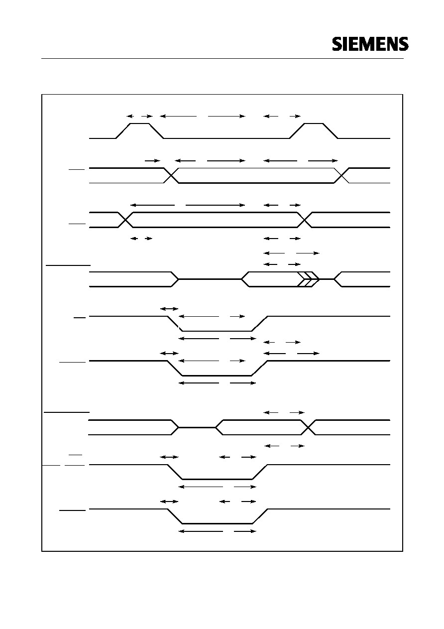
20Dec96@09:25h Intermediate Version
Semiconductor Group
58
C167CR-16RM
Figure 15-3
External Memory Cycle: Demultiplexed Bus, No Read/Write Delay, Normal ALE
AA
AA
AA
AA
AA
AA
AA
AA
AA
AA
AA
AA
AA
AA
AA
AA
AA
AA
AA
AA
AA
AA
AA
AA
AA
AA
AA
AA
AA
AA
AA
AA
AA
A
A
AA
AA
AA
AA
AA
AA
AA
AA
AA
AA
AA
AA
AA
AA
AA
A
A
A
A
A
A
A
A
A
A
A
A
Data Out
Data In
t
38
AA
AA
AA
AA
AA
AA
AA
AA
AA
AA
AA
AA
AA
AA
AA
AA
AA
AA
AA
AA
AA
AA
AA
AA
AA
AA
AA
AA
AA
AA
AA
AA
AA
AA
AA
A
AA
AA
AA
AA
AA
AA
AA
AA
AA
AA
AA
AA
AA
AA
A
A
A
A
A
A
A
A
A
A
A
A
A
A
A
A
A
A
A
A
A
A
A
A
A
A
A
A
A
A
A
A
A
A
A
AA
AA
AA
AA
AA
AA
AA
AA
AA
AA
AA
AA
AA
AA
AA
AA
AA
AA
AA
AA
AA
AA
AA
AA
A
A
A
A
A
A
A
A
A
A
A
A
A
A
A
A
A
A
A
A
A
A
A
A
A
A
A
A
A
A
A
A
A
A
A
A
A
A
A
A
A
A
A
A
A
A
A
A
A
A
A
A
A
A
A
A
A
A
A
A
A
A
A
A
A
A
A
A
A
A
A
A
A
A
A
A
A
A
A
A
A
A
A
A
A
A
A
A
A
A
A
A
A
A
A
A
A
A
A
A
AA
AA
AA
AA
AA
AA
AA
AA
AA
AA
AA
AA
AA
AA
AA
AA
AA
AA
AA
AA
AA
AA
AA
AA
AA
AA
AA
AA
AA
AA
AA
AA
AA
AA
AA
AA
AA
AA
AA
AA
A
A
A
A
A
A
A
A
A
A
A
A
A
A
A
A
A
A
A
A
A
A
A
A
A
A
A
A
A
A
A
A
A
A
A
A
A
A
A
A
A
A
A
A
A
A
A
A
A
A
A
A
A
A
A
A
A
A
A
A
A
A
A
A
A
A
A
A
A
A
A
A
A
A
A
A
A
A
A
A
A
A
A
A
A
A
A
A
A
A
A
A
A
A
A
A
A
A
A
A
A
A
A
A
A
A
A
A
A
A
A
A
A
A
A
A
A
A
A
A
A
A
A
A
A
A
A
A
A
A
A
A
A
A
A
A
A
A
A
A
A
A
A
A
A
A
A
A
A
A
A
A
A
A
A
A
A
A
A
A
A
A
A
A
A
A
A
A
A
A
A
A
A
A
A
A
A
A
A
A
A
A
A
A
A
A
A
A
A
A
A
AA
A
AA
AA
AA
AA
AA
AA
AA
AA
AA
AA
AA
AA
AA
AA
AA
AA
AA
AA
AA
AA
AA
AA
AA
AA
AA
AA
AA
AA
AA
AA
AA
AA
AA
AA
AA
AA
AA
AA
AA
AA
AA
AA
AA
AA
AA
AA
AA
AA
AA
AA
AA
AA
AA
AA
AA
AA
AA
AA
AA
AA
AA
AA
AA
AA
AA
AA
AA
AA
AA
AA
AA
AA
AA
AA
AA
AA
AA
AA
AA
AA
AA
AA
AA
AA
AA
AA
AA
AA
AA
A
A
A
A
A
A
A
A
A
A
A
A
A
AA
A
AA
AA
AA
AA
AA
AA
AA
AA
AA
AA
AA
AA
AA
AA
AA
AA
AA
AA
AA
AA
AA
AA
AA
AA
AA
AA
AA
AA
AA
AA
AA
AA
AA
AA
AA
AA
AA
AA
AA
AA
AA
AA
AA
AA
AA
AA
AA
AA
AA
AA
AA
AA
AA
AA
AA
AA
AA
AA
AA
AA
AA
AA
AA
AA
AA
AA
AA
AA
AA
AA
AA
AA
AA
AA
AA
AA
AA
AA
AA
AA
AA
AA
AA
AA
AA
AA
AA
AA
AA
AA
AA
AA
AA
AA
AA
AA
AA
AA
AA
AA
AA
AA
AA
AA
AA
AA
AA
AA
AA
AA
AA
AA
AA
AA
AA
AA
AA
AA
AA
AA
AA
AA
AA
AA
AA
AA
AA
AA
AA
AA
AA
AA
AA
AA
AA
AA
AA
AA
Address
ALE
CSx
A23-A16
A15-A0
BHE
Read Cycle
RD
RdCSx
Write Cycle
WrCSx
t
5
t
16
t
17
t
6
t
39
t
41
t
26
t
28
t
18
t
21
A
A
A
A
A
A
A
A
A
A
A
A
A
A
A
A
t
15
t
47
t
13
t
49
t
22
t
24
t
13
t
49
t
9
t
43
t
43
t
9
t
50
t
51
t
55
t
68
t
57
BUS
(D15-D8)
D7-D0
BUS
(D15-D8)
D7-D0
WR,
WRL, WRH
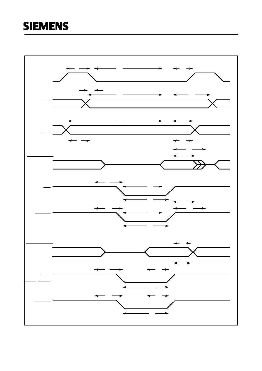
20Dec96@09:25h Intermediate Version
59
Semiconductor Group
C167CR-16RM
Figure 15-4
External Memory Cycle: Demultiplexed Bus, No Read/Write Delay, Extended ALE
A
A
A
A
A
A
A
A
A
A
A
A
A
A
A
A
A
A
A
A
A
A
A
A
A
A
A
A
A
A
A
A
A
AA
AA
AA
AA
AA
AA
AA
AA
AA
AA
AA
AA
AA
AA
AA
AA
A
A
AA
AA
AA
AA
AA
AA
AA
AA
AA
AA
AA
AA
AA
AA
AA
A
A
A
A
A
A
A
A
A
A
A
A
Data Out
Data In
t
38
AA
AA
AA
AA
AA
AA
AA
AA
AA
AA
AA
AA
AA
AA
AA
AA
AA
AA
AA
AA
AA
AA
AA
AA
AA
AA
AA
AA
AA
AA
AA
AA
AA
AA
AA
AA
AA
AA
AA
AA
AA
AA
AA
AA
AA
AA
AA
AA
AA
AA
AA
AA
AA
AA
AA
AA
AA
AA
AA
AA
AA
AA
AA
AA
AA
AA
AA
AA
AA
AA
AA
AA
AA
AA
AA
AA
AA
AA
AA
AA
AA
AA
AA
AA
AA
AA
AA
AA
AA
AA
AA
AA
AA
AA
AA
AA
AA
AA
AA
AA
AA
AA
AA
AA
AA
AA
AA
AA
AA
AA
AA
AA
AA
AA
AA
AA
AA
AA
AA
AA
AA
AA
AA
AA
AA
AA
AA
AA
A
A
A
A
A
A
A
A
A
A
A
A
A
A
A
A
A
A
A
A
A
A
A
A
A
A
A
A
A
A
A
A
A
A
A
A
A
A
A
A
A
A
A
A
A
A
A
A
A
A
A
A
A
A
A
A
A
A
A
A
A
A
A
A
A
A
A
A
A
A
A
A
A
A
A
A
A
A
A
A
AA
AA
AA
AA
AA
AA
AA
AA
AA
AA
AA
AA
AA
AA
AA
AA
AA
AA
AA
AA
AA
AA
AA
AA
AA
AA
AA
AA
AA
AA
AA
AA
AA
AA
AA
AA
AA
AA
AA
AA
A
A
A
A
A
A
A
A
A
A
A
A
A
A
A
A
A
A
A
A
A
A
A
A
A
A
A
A
A
A
A
A
A
A
A
A
A
A
A
A
A
A
AA
A
AA
AA
AA
AA
AA
AA
AA
AA
AA
AA
AA
AA
AA
AA
AA
AA
AA
AA
AA
AA
AA
AA
AA
AA
AA
AA
AA
AA
AA
AA
AA
AA
AA
AA
AA
AA
AA
AA
AA
AA
AA
AA
AA
AA
AA
AA
AA
AA
AA
AA
AA
AA
AA
AA
AA
AA
AA
AA
AA
AA
AA
AA
AA
AA
AA
AA
AA
AA
AA
AA
AA
AA
AA
AA
AA
AA
AA
AA
AA
AA
AA
AA
AA
AA
AA
AA
AA
AA
AA
AA
AA
AA
AA
AA
AA
AA
AA
AA
AA
AA
AA
AA
AA
AA
AA
AA
AA
AA
AA
AA
AA
AA
AA
AA
AA
AA
AA
AA
AA
AA
AA
AA
AA
AA
AA
AA
AA
AA
AA
AA
AA
AA
AA
AA
AA
AA
AA
AA
AA
AA
AA
AA
AA
AA
A
A
A
A
A
A
A
A
A
A
A
A
A
A
A
A
A
A
A
A
A
A
A
A
A
A
A
A
A
A
A
A
A
A
A
A
A
A
A
A
A
A
A
A
A
A
A
A
A
A
A
A
A
A
A
A
A
A
A
A
A
A
A
A
A
A
A
A
A
A
A
A
A
A
A
A
A
A
A
A
A
A
A
A
A
A
A
A
A
A
A
A
A
A
A
A
A
A
A
A
A
A
A
A
A
A
AA
A
AA
AA
AA
AA
AA
AA
AA
AA
AA
AA
AA
AA
AA
AA
AA
AA
AA
AA
AA
AA
AA
AA
AA
AA
AA
AA
AA
AA
AA
AA
AA
AA
AA
AA
AA
AA
AA
AA
AA
AA
AA
AA
AA
AA
AA
AA
AA
AA
AA
AA
AA
AA
AA
AA
AA
AA
AA
AA
AA
AA
AA
AA
AA
AA
AA
AA
AA
AA
AA
AA
AA
AA
AA
AA
AA
AA
AA
AA
AA
AA
AA
AA
AA
AA
AA
AA
AA
AA
AA
AA
AA
AA
AA
AA
AA
AA
AA
AA
AA
AA
AA
AA
AA
AA
AA
AA
AA
AA
AA
AA
AA
AA
AA
AA
AA
AA
AA
AA
AA
AA
AA
AA
AA
AA
AA
AA
AA
AA
AA
AA
AA
AA
AA
AA
AA
AA
AA
AA
Address
ALE
CSx
A23-A16
A15-A0
BHE
Read Cycle
RD
RdCSx
Write Cycle
WR,
WRL, WRH
WrCSx
t
5
t
16
t
17
t
6
t
39
t
41
t
26
t
28
t
18
t
21
t
15
t
47
t
13
t
49
t
22
t
24
t
13
t
49
t
9
t
43
t
43
t
9
t
50
t
51
t
55
t
68
t
57
BUS
(D15-D8)
D7-D0
BUS
(D15-D8)
D7-D0

20Dec96@09:25h Intermediate Version
Semiconductor Group
60
C167CR-16RM
AC Characteristics
CLKOUT and READY
V
CC
= 5 V
±
10 %;
V
SS
= 0 V
T
A
= 0 to +70 ∞C
for SAB-C167CR-16RM
T
A
= -40 to +85 ∞C
for SAF-C167CR-16RM
T
A
= -40 to +125 ∞C
for SAK-C167CR-16RM
C
L
(for PORT0, PORT1, Port 4, ALE, RD, WR, BHE, CLKOUT) = 100 pF
C
L
(for Port 6, CS) = 100 pF
Notes
1)
These timings are given for test purposes only, in order to assure recognition at a specific clock edge.
2)
Demultiplexed bus is the worst case. For multiplexed bus 2TCL are to be added to the maximum values. This
adds even more time for deactivating READY.
The 2t
A
and t
C
refer to the next following bus cycle, t
F
refers to the current bus cycle.
Parameter
Symbol
Max. CPU Clock
= 20 MHz
Variable CPU Clock
1/2TCL = 1 to 20 MHz
Unit
min.
max.
min.
max.
CLKOUT cycle time
t
29
CC
50
50
2TCL
2TCL
ns
CLKOUT high time
t
30
CC
20
≠
TCL ≠ 5
≠
ns
CLKOUT low time
t
31
CC
15
≠
TCL ≠ 10
≠
ns
CLKOUT rise time
t
32
CC
≠
5
≠
5
ns
CLKOUT fall time
t
33
CC
≠
5
≠
5
ns
CLKOUT rising edge to
ALE falling edge
t
34
CC
0 +
t
A
10 +
t
A
0 +
t
A
10 +
t
A
ns
Synchronous READY
setup time to CLKOUT
t
35
SR
15
≠
15
≠
ns
Synchronous READY
hold time after CLKOUT
t
36
SR
0
≠
0
≠
ns
Asynchronous READY
low time
t
37
SR
65
≠
2TCL + 15
≠
ns
Asynchronous READY
setup time
1)
t
58
SR
15
≠
15
≠
ns
Asynchronous READY
hold time
1)
t
59
SR
0
≠
0
≠
ns
Async. READY hold time
after RD, WR high
(Demultiplexed Bus)
2)
t
60
SR
0
0
+ 2
t
A
+
t
C
+
t
F
2)
0
TCL - 25
+
2
t
A
+
t
C
+
t
F
2)
ns
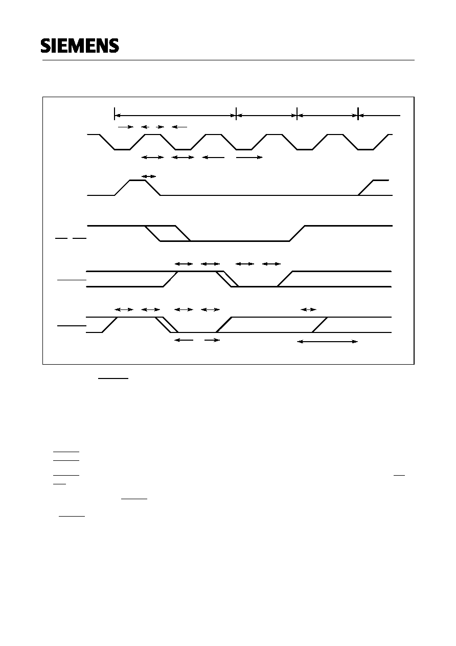
20Dec96@09:25h Intermediate Version
61
Semiconductor Group
C167CR-16RM
Figure 16
CLKOUT and READY
Notes
1)
Cycle as programmed, including MCTC waitstates (Example shows 0 MCTC WS).
2)
The leading edge of the respective command depends on RW-delay.
3)
READY sampled HIGH at this sampling point generates a READY controlled waitstate,
READY sampled LOW at this sampling point terminates the currently running bus cycle.
4)
READY may be deactivated in response to the trailing (rising) edge of the corresponding command (RD or
WR).
5)
If the Asynchronous READY signal does not fulfill the indicated setup and hold times with respect to CLKOUT
(eg. because CLKOUT is not enabled), it must fulfill
t
37
in order to be safely synchronized. This is guaranteed,
if READY is removed in reponse to the command (see Note
4)
).
6)
Multiplexed bus modes have a MUX waitstate added after a bus cycle, and an additional MTTC waitstate may
be inserted here.
For a multiplexed bus with MTTC waitstate this delay is 2 CLKOUT cycles, for a demultiplexed bus without
MTTC waitstate this delay is zero.
7)
The next external bus cycle may start here.
A
A
AA
AA
AA
AA
AA
AA
AA
AA
AA
AA
A
A
A
A
A
A
A
A
A
A
A
A
AA
AA
AA
AA
AA
AA
AA
AA
AA
AA
AA
AA
A
A
A
A
A
A
A
A
A
A
A
A
AAAA
AAAA
AAAA
AAAA
AAAA
AAAA
AAAA
AAAA
AAAA
AAAA
AAAA
AAAA
AAAA
AAAA
AAAA
AAAA
AAAA
AAAA
AAAA
AAAA
AAAA
AAAA
AAAA
AAAA
AAAA
AAAA
AAAA
AAAA
AAAA
AAAA
AAAA
AAAA
AAAA
AAAA
AAAA
AAAA
AAAA
AAAA
AAAA
AAAA
AAAA
AAAA
AAAA
AAAA
AAAA
AAAA
AAAA
AAAA
AAAA
AAAA
AAAA
AAAA
AAAA
AAAA
AA
AA
AA
AA
AA
AA
AA
AA
AA
AA
AA
AA
AA
AA
AA
AA
AA
AA
AA
AA
AA
AA
AA
AA
AA
AA
AA
AA
AA
AA
AA
AA
AA
AA
AA
AA
AA
AA
AA
AA
AA
AA
AA
AA
AA
AA
AA
AA
AA
AA
AA
AA
AA
AA
AA
AA
AA
AA
AA
AA
AA
AA
AA
AA
AA
AA
AA
AA
AA
AA
AA
AA
AA
AA
AA
AA
AA
AA
AA
AA
AA
AA
AA
AA
AA
AA
AA
AA
AA
AA
AA
AA
AA
AA
AA
AA
AA
AA
AA
AA
AA
AA
AA
AA
AA
AA
AA
AA
AA
AA
AA
AA
AA
AA
AA
AA
AA
AA
AA
AA
AA
AA
AA
AA
AA
AA
AA
AA
AA
AA
AA
AA
AA
AA
AA
AA
AA
AA
AA
AA
AA
AA
AA
AA
AA
AA
AA
AA
AA
AA
AA
AA
AA
AA
AA
AA
AA
AA
AA
A
A
A
A
A
A
A
A
A
A
A
A
A
A
A
A
A
A
A
A
A
A
A
A
A
A
A
A
A
A
A
A
A
A
A
A
A
A
A
A
A
A
A
A
A
A
A
A
A
A
A
A
A
A
A
A
A
A
A
A
A
A
A
A
A
A
A
A
A
A
A
A
A
A
A
A
A
A
A
A
A
A
A
AA
AA
AA
AA
AA
AA
AA
AA
AA
AA
AA
AA
AA
AA
AA
A
A
A
A
A
A
A
A
A
A
A
A
A
A
A
A
A
A
A
A
A
A
A
A
A
A
A
A
A
A
A
A
A
A
A
A
A
A
A
A
A
A
A
A
A
A
A
A
A
A
A
A
A
A
A
A
A
A
A
A
A
A
A
A
AA
AA
AA
AA
AA
AA
AA
AA
AA
AA
AA
AA
AA
AA
AA
AA
AA
AA
AA
AA
AA
AA
AA
AA
AA
AA
AA
AA
AA
AA
AA
AA
AA
AA
AA
AA
AA
AA
AA
AA
AA
AA
AA
AA
AA
AA
AA
AA
AA
AA
AA
AA
AA
AA
AA
AA
AA
AA
AA
AA
AA
AA
AA
AA
A
AA
AA
AA
AA
AA
AA
AA
AA
AA
AA
AA
AA
AA
AA
AA
AA
AA
AA
AA
AA
AA
AA
AA
AA
AA
AA
AA
AA
AA
AA
AA
AA
AA
AA
AA
AA
AA
AA
AA
AA
AA
AA
AA
AA
AA
AA
AA
AA
AA
AA
AA
AA
AA
AA
AA
AA
AA
AA
AA
AA
AA
AA
AA
AA
AA
AA
AA
AA
A
A
A
A
A
A
A
A
A
A
A
A
A
A
A
A
A
A
A
A
A
A
A
A
A
A
A
A
A
A
A
A
A
A
A
A
A
A
A
A
A
A
A
A
A
A
A
A
A
A
A
A
A
A
A
A
A
A
A
A
A
A
A
A
A
A
A
A
A
A
A
A
A
A
A
A
A
A
A
A
A
A
A
A
AA
AA
AA
AA
AA
AA
AA
AA
AA
AA
AA
AA
AA
AA
AA
AA
AA
AA
AA
AA
AA
AA
AA
AA
AA
AA
AA
AA
AA
AA
AA
AA
AA
A
A
A
A
A
A
A
A
A
A
A
A
A
A
A
A
A
A
A
A
A
A
A
A
A
A
A
A
A
A
A
A
A
AA
AA
AA
AA
AA
AA
AA
AA
AA
AA
AA
AA
AA
AA
AA
AA
AA
AA
AA
AA
AA
AA
AA
AA
AA
AA
AA
AA
AA
AA
AA
AA
AA
AA
AA
AA
AA
AA
AA
AA
AA
AA
AA
AA
AA
AA
AA
AA
AA
AA
AA
AA
AA
AA
AA
AA
AA
AA
AA
AA
AA
AA
AA
AA
AA
AA
AA
AA
AA
AA
AA
AA
AA
AA
AA
AA
AA
AA
AA
AA
AA
AA
AA
AA
AA
AA
A
A
A
A
A
A
A
A
A
A
A
CLKOUT
A
A
AA
AA
AA
AA
AA
AA
AA
AA
AA
AA
ALE
t
30
t
34
Sync
READY
t
35
t
36
t
35
t
36
Async
READY
t
58
t
59
t
58
t
59
waitstate
READY
MUX/Tristate
6)
t
32
t
33
t
29
Running cycle
1)
t
31
t
37
3)
3)
5)
Command
RD, WR
t
60
4)
see 6)
2)
7)
3)
3)
20Dec96@09:25h Intermediate Version
Semiconductor Group
62
C167CR-16RM
AC Characteristics
External Bus Arbitration
V
CC
= 5 V
±
10 %;
V
SS
= 0 V
T
A
= 0 to +70 ∞C
for SAB-C167CR-16RM
T
A
= -40 to +85 ∞C
for SAF-C167CR-16RM
T
A
= -40 to +125 ∞C
for SAK-C167CR-16RM
C
L
(for PORT0, PORT1, Port 4, ALE, RD, WR, BHE, CLKOUT) = 100 pF
C
L
(for Port 6, CS) = 100 pF
Parameter
Symbol
Max. CPU Clock
= 20 MHz
Variable CPU Clock
1/2TCL = 1 to 20 MHz
Unit
min.
max.
min.
max.
HOLD input setup time
to CLKOUT
t
61
SR
20
≠
20
≠
ns
CLKOUT to HLDA high
or BREQ low delay
t
62
CC
≠
20
≠
20
ns
CLKOUT to HLDA low
or BREQ high delay
t
63
CC
≠
20
≠
20
ns
CSx release
t
64
CC
≠
20
≠
20
ns
CSx drive
t
65
CC
-5
25
-5
25
ns
Other signals release
t
66
CC
≠
20
≠
20
ns
Other signals drive
t
67
CC
-5
25
-5
25
ns
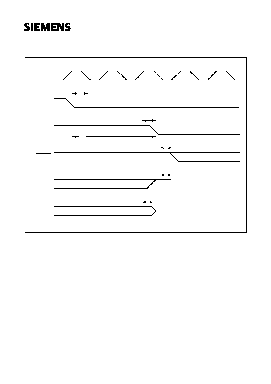
20Dec96@09:25h Intermediate Version
63
Semiconductor Group
C167CR-16RM
Figure 17
External Bus Arbitration, Releasing the Bus
Notes
1)
The C167CR-16RM will complete the currently running bus cycle before granting bus access.
2)
This is the first possibility for BREQ to get active.
3)
The CS outputs will be resistive high (pullup) after
t
64
.
AA
AA
AA
AA
AA
AA
AA
AA
AA
AA
AA
AA
A
A
A
A
A
A
A
A
A
A
A
A
A
A
A
A
A
A
A
A
A
A
A
A
A
A
A
A
A
A
A
A
A
A
A
A
A
A
A
A
AA
AA
AA
AA
AA
AA
AA
AA
AA
AA
AA
AA
AA
AA
AA
AA
AA
AA
AA
AA
AA
AA
AA
AA
AA
AA
AA
AA
AA
AA
AA
AA
AA
AA
AA
AA
AA
AA
AA
AA
AA
AA
AA
AA
AA
AA
AA
AA
AA
AA
AA
AA
AA
AA
AA
AA
AA
AA
AA
AA
AA
AA
AA
AA
A
A
A
A
A
A
A
A
A
A
A
A
A
A
A
A
A
A
A
A
A
A
A
A
A
A
A
A
A
A
A
A
A
A
A
A
A
A
A
A
A
A
A
A
A
A
A
A
A
A
A
A
A
A
A
A
A
A
A
A
A
A
A
A
A
A
A
A
A
A
A
A
A
A
A
A
A
A
A
A
A
A
A
A
A
A
A
A
A
A
A
A
A
A
A
A
A
A
A
A
A
A
A
A
A
A
A
A
A
A
A
A
A
A
A
A
A
A
A
A
A
A
A
A
A
A
AAAA
AAAA
AAAA
AAAA
AAAA
AAAA
AAAA
AAAA
AAAA
AAAA
AAAA
AAAA
AAAA
AAAA
AAAA
AAAA
AAAA
AAAA
AAAA
AAAA
AAAA
AAAA
AAAA
AAAA
AAAA
AAAA
AAAA
AAAA
AAAA
AAAA
AAAA
AAAA
AAAA
AAAA
AAAA
AAAA
AAAA
AAAA
AAAA
AAAA
AAAA
AAAA
AAAA
AAAA
AAAA
AAAA
AAAA
AAAA
AAAA
AAAA
AAAA
AAAA
AAAA
AAAA
AAAA
AAAA
AAAA
AAAA
AAAA
AAAA
AAAA
AAAA
AAAA
AAAA
AAAA
AAAA
AAAA
AAAA
AAAA
AAAA
AAAA
AAAA
AAAA
AAAA
AAAA
AAAA
AAAA
AAAA
AAAA
AAAA
AAAA
AAAA
AAAA
AAAA
AAAA
AAAA
AAAA
AAAA
AAAA
AAAA
AAAA
AAAA
AAAA
AAAA
AAAA
AAAA
AAAA
AAAA
AAAA
AAAA
AAAA
AAAA
AAAA
AAAA
AAAA
AAAA
AAAA
AAAA
AAAA
AAAA
AAAA
AAAA
AAAA
AAAA
AAAA
AAAA
AAAA
AAAA
AAAA
AAAA
AAAA
AAAA
AAAA
AAAA
AAAA
AAAA
AAAA
AAAA
AAAA
AAAA
AAAA
AAAA
AAAA
AAAA
AAAA
AAAA
AAAA
AAAA
AAAA
AAAA
AAAA
AAAA
AAAA
AAAA
AAAA
AAAA
AAAA
AAAA
AAAA
AAAA
AAAA
AAAA
AAAA
AAAA
AAAA
AAAA
AAAA
AAAA
AAAA
AAAA
AAAA
AAAA
AAAA
AAAA
AAAA
AAAA
AAAA
AAAA
AAAA
AAAA
AAAA
AAAA
AAAA
AAAA
AAAA
AAAA
AAAA
AAAA
AAAA
AAAA
AAAA
AAAA
AAAA
AAAA
AAAA
AAAA
AAAA
AAAA
AAAA
AAAA
AAAA
AAAA
AAAA
AAAA
AAAA
AAAA
AAAA
AAAA
AAAA
AAAA
AAAA
AAAA
AAAA
AAAA
AAAA
AAAA
AAAA
AAAA
AAAA
AAAA
AAAA
AAAA
AAAA
AAAA
AAAA
AAAA
AAAA
AAAA
AAAA
AAAA
AAAA
AAAA
AAAA
AAAA
AAAA
AAAA
AAAA
AAAA
AAAA
AAAA
AAAA
AAAA
AAAA
AAAA
AAAA
AAAA
AAAA
AAAA
AAAA
AAAA
AAAA
AAAA
AAAA
AAAA
AAAA
AAAA
AAAA
AAAA
AAAA
AAAA
AAAA
AAAA
AAAA
AAAA
AAAA
AAAA
AAAA
AAAA
AAAA
AAAA
AAAA
AAAA
AAAA
AAAA
AAAA
AAAA
AAAA
AAAA
AAAA
AAAA
AAAA
AAAA
AAAA
AAAA
AAAA
AAAA
AAAA
AAAA
AAAA
AAAA
AAAA
AAAA
AAAA
AAAA
AAAA
AAAA
AAAA
AAAA
AAAA
AAAA
AAAA
AAAA
AAAA
AAAA
AAAA
AAAA
AAAA
AAAA
AAAA
AAAA
AAAA
AAAA
AAAA
AAAA
AAAA
AAAA
AAAA
AAAA
AAAA
AAAA
AAAA
AAAA
AAAA
AAAA
AAAA
AAAA
AAAA
AAAA
AAAA
AAAA
AAAA
AAAA
AAAA
AAAA
AAAA
AAAA
AAAA
AAAA
AAAA
AAAA
AAAA
AAAA
AAAA
AAAA
AAAA
AAAA
AAAA
AAAA
AAAA
AAAA
AAAA
AAAA
AAAA
AAAA
AAAA
AAAA
AAAA
AAAA
AAAA
AAAA
AAAA
AAAA
AAAA
AAAA
AAAA
AAAA
AAAA
AAAA
AAAA
AAAA
AAAA
AAAA
AAAA
AAAA
AAAA
AAAA
AAAA
AAAA
AAAA
AAAA
AAAA
AAAA
AAAA
AAAA
AAAA
AAAA
AAAA
AAAA
AAAA
AAAA
AAAA
AAAA
AAAA
AAAA
AAAA
AAAA
AAAA
AAAA
AAAA
AAAA
AAAA
AAAA
AAAA
AAAA
AAAA
AAAA
AAAA
AAAA
AAAA
AAAA
AAAA
AAAA
AAAA
AAAA
AAAA
AAAA
AAAA
AAAA
AAAA
AAAA
AAAA
AAAA
AAAA
AAAA
AAAA
AAAA
AAAA
AAAA
AAAA
AAAA
AAAA
AAAA
AAAA
AAAA
AAAA
AAAA
AAAA
AAAA
AAAA
AAAA
AAAA
AAAA
AAAA
AAAA
AAAA
AAAA
AAAA
AAAA
AAAA
AAAA
AAAA
AAAA
AAAA
AAAA
AAAA
AA
AA
AA
AA
AA
AA
AA
AA
AA
AA
AA
AA
AA
AA
AA
AA
AA
AA
AA
AA
AA
AA
AA
AA
AA
AA
AA
AA
AA
AA
AA
AA
AA
AA
AA
AA
AA
AA
AA
AA
AA
AA
AA
AA
AA
AA
AA
AA
AA
AA
AA
AA
AA
AA
AA
AA
AA
AA
AA
AA
AA
AA
AA
AA
AA
AA
AA
AA
AA
AA
AA
AA
AA
AA
AA
AA
AA
AA
AA
AA
AA
AA
AA
AA
AA
AA
AA
AA
AA
CLKOUT
HOLD
t
61
HLDA
t
63
Other
Signals
t
66
A
AA
AAAAAAAAAAAAAAAAAAAAAAAAAAAAAAAAAAAAAAAAAAAAAAAAA
1)
CSx
(On P6.x)
t
64
1)
2)
BREQ
t
62
A
A
AAAAAAAAAAAAAAAAAAAAAAAAAAAAAAAAAAAAAAAAA
3)
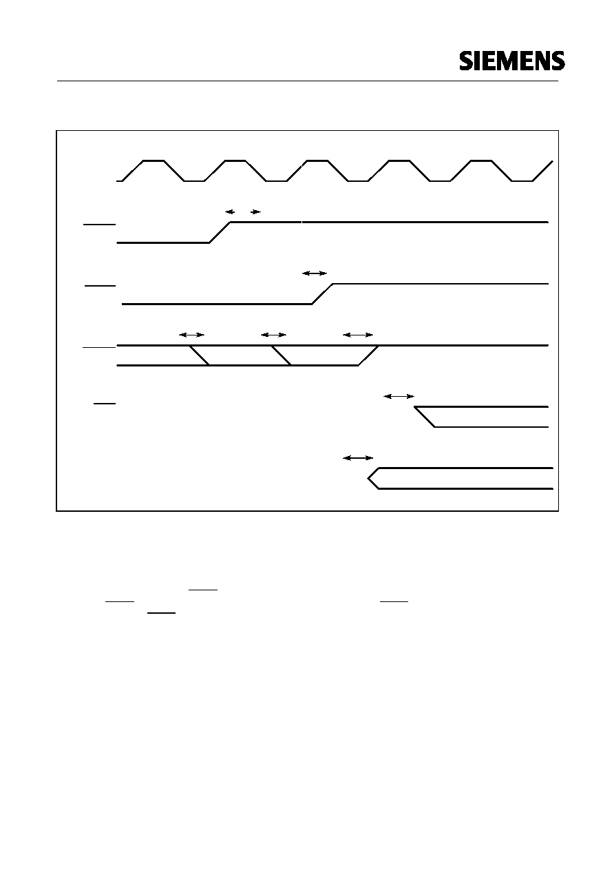
20Dec96@09:25h Intermediate Version
Semiconductor Group
64
C167CR-16RM
Figure 18
External Bus Arbitration, (Regaining the Bus)
Notes
1)
This is the last chance for BREQ to trigger the indicated regain-sequence.
Even if BREQ is activated earlier, the regain-sequence is initiated by HOLD going high.
Please note that HOLD may also be deactivated without the C167CR-16RM requesting the bus.
2)
The next C167CR-16RM driven bus cycle may start here.
AA
AA
AA
AA
AA
AA
AA
AA
AA
AA
AA
AA
A
A
A
A
A
A
A
A
A
A
A
A
A
A
A
A
A
A
A
A
A
A
A
A
AA
AA
AA
AA
AA
AA
AA
AA
AA
AA
AA
AA
A
A
A
A
A
A
A
A
A
A
A
A
AA
AA
AA
AA
AA
AA
AA
AA
AA
AA
AA
AA
AA
AA
AA
AA
AA
AA
AA
AA
AA
AA
AA
AA
AA
AA
AA
AA
AA
AA
AA
AA
AA
AA
AA
AA
AA
AA
AA
AA
AA
AA
AA
AA
AA
AA
AA
AA
AA
AA
AA
AA
AA
AA
AA
AA
AA
AA
AA
AA
AA
AA
AA
AA
AA
AA
AA
AA
AA
AA
AA
AA
AA
AA
AA
AA
AA
AA
AA
AA
AA
AA
AA
AA
AA
AA
AA
AA
AA
AA
AA
AA
AA
AA
AA
AA
AA
AA
AA
AA
AA
AA
AA
AA
AA
AA
AA
AA
AA
AA
AA
AA
AA
AA
AA
AA
AA
AA
AA
AA
AA
AA
AA
AA
AA
AA
AA
AA
AA
AA
AA
AA
AA
AA
AA
AA
AA
AA
AA
AA
AA
AA
AA
AA
AA
AA
AA
AA
AA
AA
AA
AA
AA
AA
AA
AA
AA
AA
AA
AA
AA
AA
AA
AA
AA
AA
AA
AA
AA
AA
AA
AA
AA
AA
AA
AA
AA
AA
AA
AA
AA
AA
AA
AA
AA
AA
AA
AA
AA
AA
AA
AA
AA
AA
AA
AA
AA
AA
AA
AA
AA
AA
A
A
A
A
A
A
A
A
A
A
A
A
A
A
A
A
A
A
A
A
A
A
A
A
A
A
A
A
A
A
A
A
A
A
A
A
A
A
A
A
A
A
A
A
A
A
A
A
AA
AA
AA
AA
AA
AA
AA
AA
AA
AA
AA
AA
CLKOUT
HOLD
HLDA
Other
Signals
t
62
AA
AA
AAAAAAAAAAAAAAAAAAAAAAAAAAAAAAAAAAAAAAAAAAAAAAAAAAAAAAAAAAAAAAA
CSx
(On P6.x)
AA
AA
AAAAAAAAAAAAAAAAAAAAAAAAAAAAAAAAAAAAAAAAAAAAAAAAAAAAAAAAAAAAAAAAAAAAAAAAAAA
t
67
t
62
1)
2)
t
65
t
61
BREQ
t
63
t
62
A
A
A
A
A
A
A
A
A
A
A
A
A
A
A
A
A
A
A
A
A
A
A
A
A
A
A
A
A
A
A
A
A
A
A
A
A
A
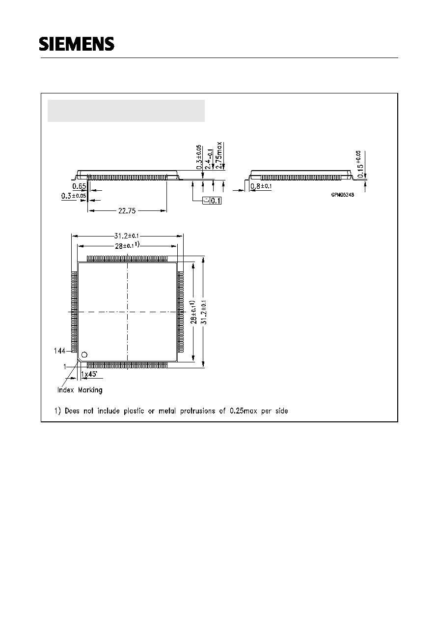
20Dec96@09:25h Intermediate Version
65
Semiconductor Group
C167CR-16RM
Package Outline
Figure 19
Sorts of Packing
Package outlines for tubes, trays, etc. are contained in our
Data Book "Package Information"
SMD = Surface Mounted Device
Dimensions in mm
Plastic Package, P-MQFP-144-1 (SMD)
(Plastic Metric Quad Flat Package)