
Data Sheet 05.96
Microcomputer Components
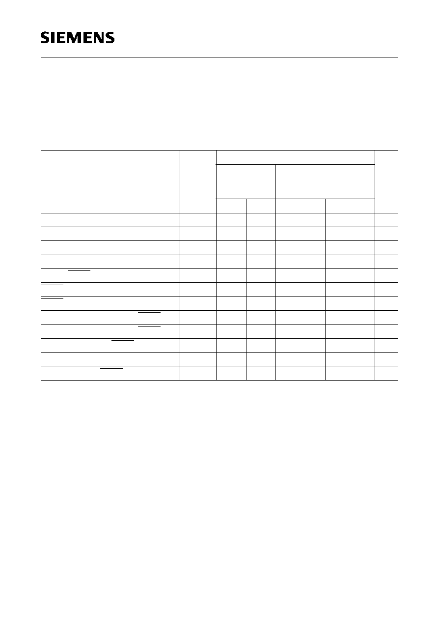
C504
8-Bit CMOS Microcontroller

Edition 05.96
This edition was realized using the software system FrameMaker
Æ
.
Published by Siemens AG,
Bereich Halbleiter, Marketing-
Kommunikation, Balanstraþe 73,
81541 M¸nchen
©
Siemens AG 1996.
All Rights Reserved.
Attention please!
As far as patents or other rights of third parties are concerned, liability is only assumed for components, not for applications, processes
and circuits implemented within components or assemblies.
The information describes the type of component and shall not be considered as assured characteristics.
Terms of delivery and rights to change design reserved.
For questions on technology, delivery and prices please contact the Semiconductor Group Offices in Germany or the Siemens Companies
and Representatives worldwide (see address list).
Due to technical requirements components may contain dangerous substances. For information on the types in question please contact
your nearest Siemens Office, Semiconductor Group.
Siemens AG is an approved CECC manufacturer.
Packing
Please use the recycling operators known to you. We can also help you ≠ get in touch with your nearest sales office. By agreement we
will take packing material back, if it is sorted. You must bear the costs of transport.
For packing material that is returned to us unsorted or which we are not obliged to accept, we shall have to invoice you for any costs in-
curred.
Components used in life-support devices or systems must be expressly authorized for such purpose!
Critical components
1
of the Semiconductor Group of Siemens AG, may only be used in life-support devices or systems
2
with the express
written approval of the Semiconductor Group of Siemens AG.
1 A critical component is a component used in a life-support device or system whose failure can reasonably be expected to cause the
failure of that life-support device or system, or to affect its safety or effectiveness of that device or system.
2 Life support devices or systems are intended (a) to be implanted in the human body, or (b) to support and/or maintain and sustain hu-
man life. If they fail, it is reasonable to assume that the health of the user may be endangered.
C504
Revision History:
Current Version: 05.96
Previous Version:
Page
(in previous
Version)
Page
( i n n e w
Version)
Subjects (major changes since last revision)
8-Bit CMOS Microcontroller
C504
Advance Information
Semiconductor Group
3
05.96
∑
Fully compatible to standard 8051 microcontroller
∑
Up to 40 MHz operating frequency
∑
16 K
◊
8 ROM (C504-2R only, optional ROM protection)
∑
256
◊
8 RAM
∑
256
◊
8 XRAM
∑
Four 8-bit ports, (2 ports with mixed analog/digital I/O capability)
∑
Three 16-bit timers/counters (timer 2 with up/down counter feature)
∑
Capture/compare unit for PWM signal generation and signal capturing
- 3-channel, 16-bit capture/compare unit
- 1-channel, 10-bit compare unit
∑
Compare unit
∑
USART
∑
10-bit A/D Converter with 8 multiplexed inputs
∑
Twelve interrupt sources with two priority levels
∑
On-chip emulation support logic (Enhanced Hooks Technology
TM
)
∑
Programmable 15-bit Watchdog Timer
∑
Oscillator Watchdog
∑
Fast Power On Reset
∑
Power Saving Modes
∑
M-QFP-44 package
∑
Temperature ranges: SAB-C504
T
A
: 0 to 70
∞
C
SAF-C504
T
A
: ≠ 40 to 85
∞
C
SAH-C504
T
A
: ≠ 40 to 110
∞
C (max. operating frequency.: TBD)
SAK-C504
T
A
: ≠ 40 to 125
∞
C (max. operating frequency.: 12 MHz)
C504
Semiconductor Group
4
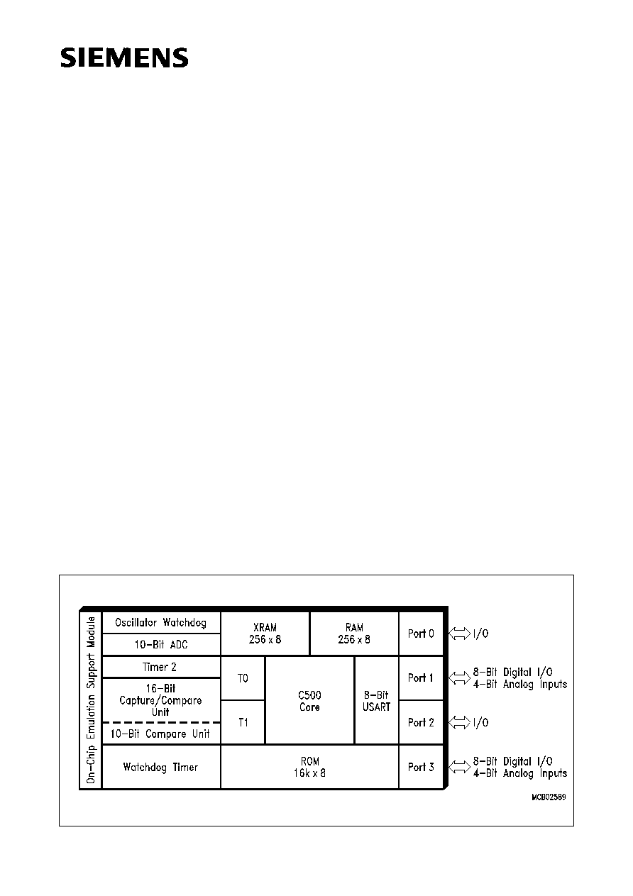
The C504 with its capture compare unit (CCU) especially provides a functionality, which allows to
use the microcontroller in motor control applications. Further, the C504 is functionally upward
compatible with the SAB 80C52/C501 microcontroller and can replace it in existing applications.
The C504-2R contains a non-volatile 16K
◊
8 read-only program memory, a volatile on-chip 512
◊
8
read/write data memory, four 8-bit wide ports, three 16-bit timers/counters, a 16-bit capture/
compare unit with compare timer, a 10-bit compare timer, a twelve source, two priority level interrupt
structure, a serial port, versatile fail save mechanisms, on-chip emulation support logic, and a
genuine 10-bit A/D converter. The C504-L is identical to the C504-2R, except that it lacks the
program memory on chip. Therefore, the term C504 refers to all versions within this data sheet
unless otherwise noted.
Note: Versions for extended temperature ranges ≠ 40 ∞C to 110 ∞C (SAH-C504) and ≠ 40 ∞C to
125 ∞C (SAK-C504) are available on request.
The ordering number of ROM types (DXXXX extensions) is defined after program release
(verification) of the customer.
Ordering Information
Type
Ordering Code
Package
Description
(8-Bit CMOS microcontroller)
SAB-C504-LM
Q67120-C1048
P-MQFP-44 for external memory (12 MHz)
SAB-C504-L24M
Q67120-C1049
P-MQFP-44 for external memory (24 MHz)
SAB-C504-L40M
Q67120-C1050
P-MQFP-44 for external memory (40 MHz)
SAB-C504-2RM
Q67120-DXXXX
P-MQFP-44 with mask-programmable ROM (12 MHz)
SAB-C504-2R24M
Q67120-DXXXX
P-MQFP-44 with mask-programmable ROM (24 MHz)
SAB-C504-2R40M
Q67120-DXXXX
P-MQFP-44 with mask-programmable ROM (40 MHz)
Semiconductor Group
5
C504
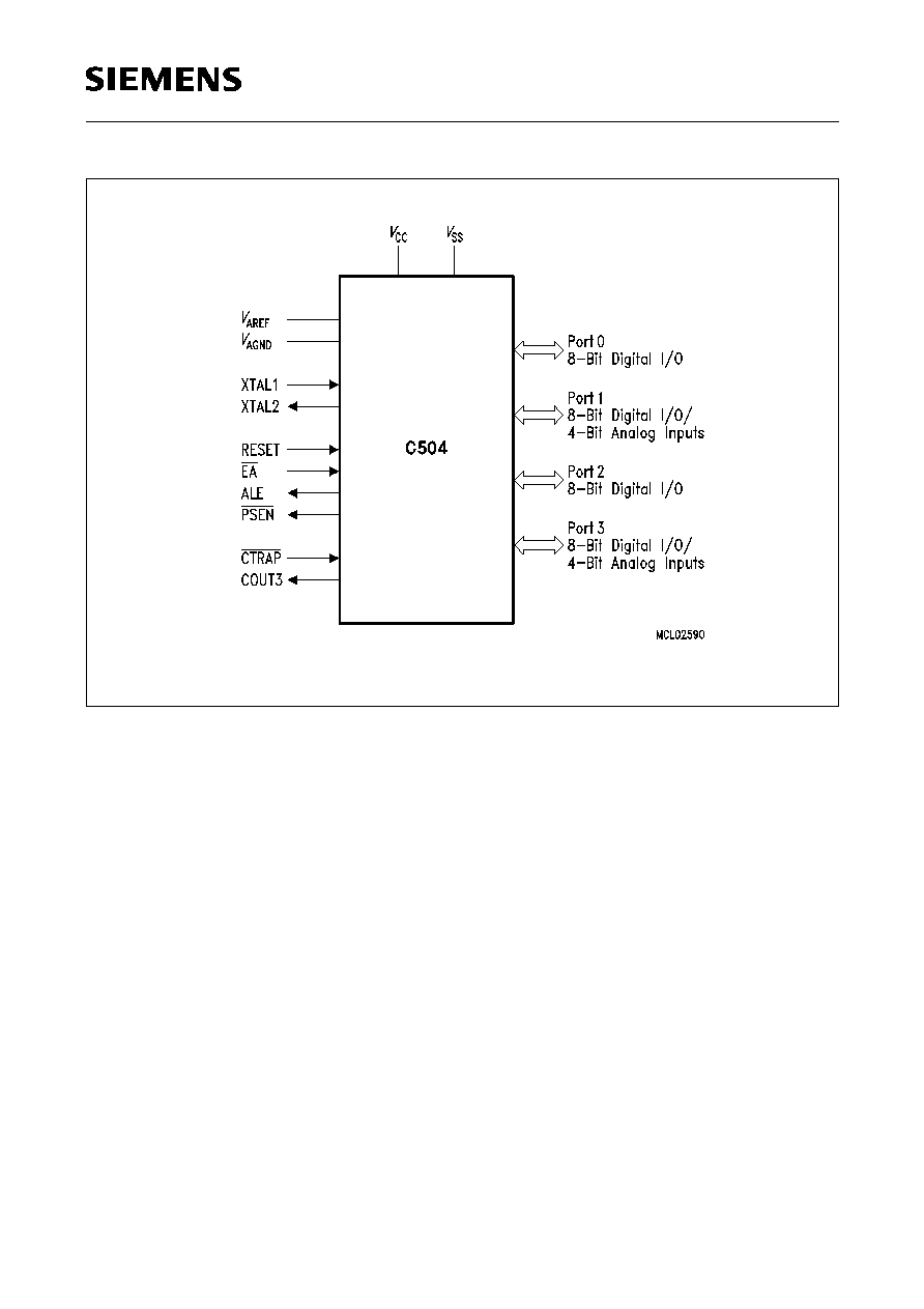
Figure 1
Logic Symbol
C504
Semiconductor Group
6
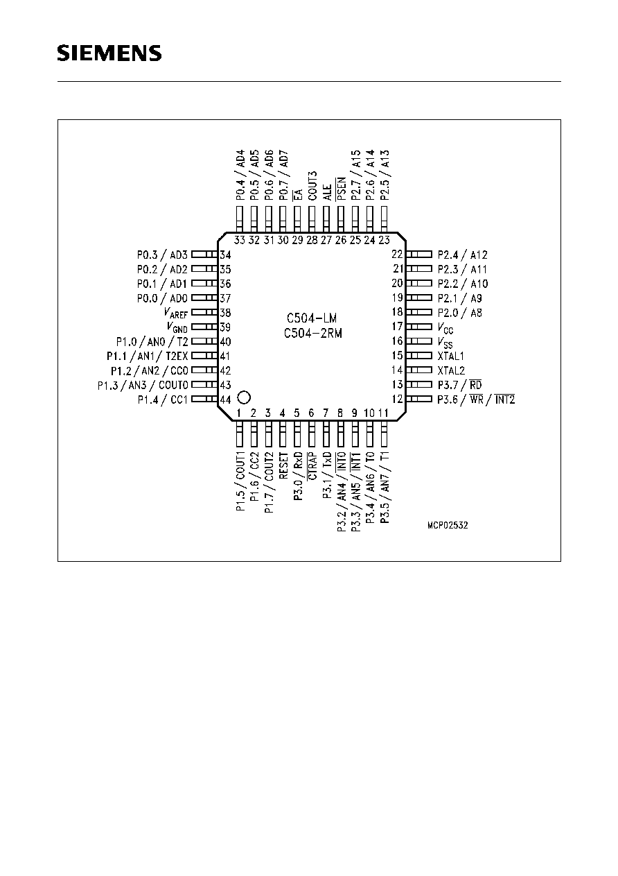
Figure 2
Pin Configuration (top view)
Semiconductor Group
7
C504
Table 1
Pin Definitions and Functions
Symbol
Pin Number
(P-MQFP-44)
I/O
*)
Function
P1.0-P1.7
40-44,
1-3
40
41
42
43
44
1
2
3
I/O
Port 1
is an 8-bit bidirectional port. Port pins can be used for
digital input/output. P1.0 - P1.3 can also be used as analog
inputs of the A/D-converter. As secondary digital functions,
port 1 contains the timer 2 pins and the capture/compare
inputs/outputs. Port 1 pins are assigned to be used as
analog inputs via the register P1ANA.
The functions are assigned to the pins of port 1 as follows:
P1.0 / AN0 / T2
Analog input channel 0 /
input to counter 2
P1.1 / AN1 / T2EX
Analog input channel 1 /
capture/reload trigger of timer 2 /
up-down count
P1.2 / AN2 / CC0
Analog input channel 2 /
input/output of capture/compare
channel 0
P1.3 / AN3 / COUT0
Analog input channel 3 /
output of capture/compare
channel 0
P1.4 / CC1
Input/output of capture/compare
channel 1
P1.5 / COUT1
Output of capture/compare
channel 1
P1.6 / CC2
Input/output of capture/compare
channel 2
P1.7 / COUT2
Output of capture/compare
channel 2
RESET
4
I
RESET
A high level on this pin for one machine cycle while the
oscillator is running resets the device. An internal diffused
resistor to
V
SS
permits power-on reset using only an
external capacitor to
V
CC
.
*)
I = Input
O = Output
C504
Semiconductor Group
8
P3.0-P3.7
5, 7-13
5
7
8
9
10
11
12
13
I/O
Port 3
is an 8-bit bidirectional port. P3.0 (R
◊
D) and P3.1 (T
◊
D)
operate as defined for the C501. P3.2 to P3.7 contain the
external interrupt inputs, timer inputs, input and as an
additional optinal function four of the analog inputs of the
A/D-converter. Port 3 pins are assigned to be used as
analog inputs via the bits of SFR P3ANA.
P3.6/WR can be assigned as a third interrupt input. The
functions are assigned to the pins of port 3 as follows:
P3.0 / RxD
Receiver data input (asynch.) or data
input/output (synch.) of serial
interface
P3.1 / TxD
Transmitter data output (asynch.) or
clock output (synch.) of serial
interface
P3.2 / AN4 / INT0
Analog input channel 4 / external
interrupt 0 input / timer 0 gate control
input
P3.3 / AN5 / INT1
Analog input channel 5 / external
interrupt 1 input / timer 1 gate control
input
P3.4 / AN6 / T0
Analog input channel 6 / timer 0
counter input
P3.5 / AN7 / T1
Analog input channel 7 / timer 1
counter input
P3.6 / WR / INT2
WR control output; latches the data
byte from port 0 into the external data
memory /
external interrupt 2 input
P3.7 / RD
RD control output; enables the
external data memory
CTRAP
6
I
CCU Trap Input
With CTRAP = low the compare outputs of the CAPCOM
unit are switched to the logic level as defined in the COINI
register (if they are enabled by the bits in SFR TRCON).
CTRAP is an input pin with an internal pullup resistor. For
power saving reasons, the signal source which drives the
CTRAP input should be at high or floating level during
power-down mode.
*)
I = Input
O = Output
Table 1
Pin Definitions and Functions (cont'd)
Symbol
Pin Number
(P-MQFP-44)
I/O
*)
Function

Semiconductor Group
9
C504
XTAL2
14
≠
XTAL2
Output of the inverting oscillator amplifier.
XTAL1
15
≠
XTAL1
Input to the inverting oscillator amplifier and input to the
internal clock generator circuits.
To drive the device from an external clock source, XTAL1
should be driven, while XTAL2 is left unconnected. There
are no requirements on the duty cycle of the external clock
signal, since the input to the internal clocking circuitry is
divided down by a divide-by-two flip-flop. Minimum and
maximum high and low times as well as rise/fall times
specified in the AC characteristics must be observed.
P2.0-P2.7
18-25
I/O
Port 2
is a bidirectional I/O port with internal pullup resistors. Port
2 pins that have 1s written to them are pulled high by the
internal pullup resistors, and in that state can be used as
inputs. As inputs, port 2 pins being externally pulled low
will source current (
I
IL
, in the DC characteris-tics) because
of the internal pullup resistors. Port 2 emits the high-order
address byte during fetches from external program
memory and during accesses to external data memory that
use 16-bit addresses (MOVX @DPTR). In this application
it uses strong internal pullup resistors when issuing 1s.
During accesses to external data memory that use 8-bit
addresses (MOVX @Ri), port 2 issues the contents of the
P2 special function register.
PSEN
26
O
The Program Store Enable
output is a control signal that enables the external program
memory to the bus during external fetch operations. It is
activated every six oscillator periodes except during
external data memory accesses. Remains high during
internal program execution.
ALE
27
O
The Address Latch Enable
output is used for latching the low-byte of the address into
external memory during normal operation. It is activated
every six oscillator periodes except during an external data
memory access. When instructions are executed from
internal ROM (EA=1) the ALE generation can be disabled
by bit EALE in SFR SYSCON.
*)
I = Input
O = Output
Table 1
Pin Definitions and Functions (cont'd)
Symbol
Pin Number
(P-MQFP-44)
I/O
*)
Function
C504
Semiconductor Group
10
COUT3
28
O
10-Bit compare channel output
This pin is used for the output signal of the 10-bit compare
timer 2 unit. COUT3 can be disabled and set to a high or
low state.
EA
29
I
External Access Enable
When held at high level, instructions are fetched from the
internal ROM (C504-2R only) when the PC is less than
4000H.When held at low level, the C504 fetches all
instructions from external program memory.
For the C504-L this pin must be tied low.
P0.0-P0.7
37-30
I/O
Port 0
is an 8-bit open-drain bidirectional I/O port. Port 0 pins that
have 1s written to them float, and in that state can be used
as high-impendance inputs.Port 0 is also the multiplexed
low-order address and data bus during accesses to
external program or data memory. In this application it
uses strong internal pullup resistors when issuing 1 s.
Port 0 also outputs the code bytes during program
verification in the C504-2R. External pullup resistors are
required during program (ROM) verification.
V
AREF
38
≠
Reference voltage for the A/D converter.
V
AGND
39
≠
Reference ground for the A/D converter.
V
SS
16
≠
Ground (0V)
V
CC
17
≠
Power Supply (+5V)
*)
I = Input
O = Output
Table 1
Pin Definitions and Functions (cont'd)
Symbol
Pin Number
(P-MQFP-44)
I/O
*)
Function
Semiconductor Group
11
C504
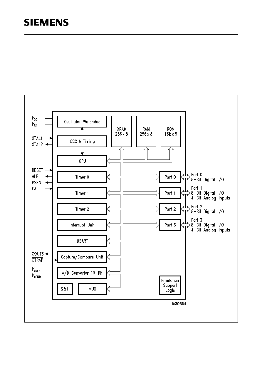
Functional Description
The C504 basic architecture is fully compatible to the standard 8051 microcontroller family. While
maintaining all architectural and operational characteristics of the SAB 80C52 / C501, the C504
incorporates some enhancements such as on-chip XRAM, A/D converter, fail save mechanisms,
and a versatile capture/compare unit.
Figure 3 shows a block diagram of the C504.
Figure 3
Block Diagram of the C504
C504
Semiconductor Group
12
CPU
The C504 is efficient both as a controller and as an arithmetic processor. It has extensive facilities
for binary and BCD arithmetic and excels in its bit-handling capabilities. Efficient use of program
memory results from an instruction set consisting of 44 % one-byte, 41 % two-byte, and 15 % three-
byte instructions. With a 12 MHz crystal, 58 % of the instructions are executed in 1.0
µ
s
(
24 MHz:
500 ns, 40 MHz : 300 ns).
Special Function Register PSW (Address D0H)
Reset Value : 00H
Bit
Function
CY
Carry Flag
Used by arithmetic instruction.
AC
Auxiliary Carry Flag
Used by instructions which execute BCD operations.
F0
General Purpose Flag
RS1
RS0
Register Bank select control bits
These bits are used to select one of the four register banks.
OV
Overflow Flag
Used by arithmetic instruction.
F1
General Purpose Flag
P
Parity Flag
Set/cleared by hardware after each instruction to indicate an odd/even
number of "one" bits in the accumulator, i.e. even parity.
CY
AC
F0
RS1
RS0
OV
F1
P
D0H
PSW
D7H
D6H
D5H
D4H
D3H
D2H
D1H
D0H
Bit No.
MSB
LSB
RS1
RS0
Function
0
0
Bank 0 selected, data address 00H-07H
0
1
Bank 1 selected, data address 08H-0FH
1
0
Bank 2 selected, data address 10H-17H
1
1
Bank 3 selected, data address 18H-1FH
Semiconductor Group
13
C504
Memory Organization
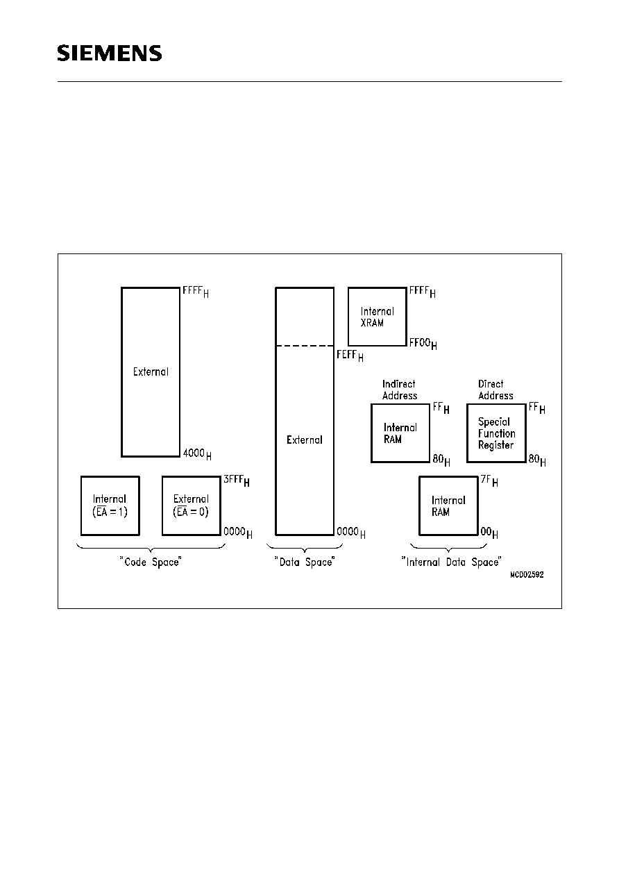
The C504 CPU manipulates operands in the following four address spaces:
≠ up to 64 Kbyte of external program memory
≠ up to 64 Kbyte of external data memory
≠ 256 bytes of internal data memory
≠ 256 bytes of internal XRAM data memory
≠ a 128 byte special function register area
Figure 4 illustrates the memory address spaces of the C504.
Figure 4
C504 Memory Map
The XRAM in the C504 is a memory area that is logically located at the upper end of the external
memory space, but is integrated on the chip. Because the XRAM is used in the same way as
external data memory the same instruction types (MOVX instructions) must be used for accessing
the XRAM. The XRAM can be enabled and disabled by the XMAP bit in the SYSCON register.
ROM Protection
The C504-2R ROM version allows to protect the content of the internal ROM against read out by
non authorized people. The type of ROM protection (protected or unprotected) is fixed with the
ROM mask. Therefore, the customer of a C504-2R ROM version has to define whether ROM
protection has to be selected or not.

C504
Semiconductor Group
14
Special Function Registers
All registers, except the program counter and the four general purpose register banks, reside in the
special function register area.
The 63 special function register (SFR) include pointers and registers that provide an interface
between the CPU and the other on-chip peripherals. There are also 128 directly addressable bits
within the SFR area.
The SFRs of the C504 are listed in table 2 and table 3. In table 2 they are organized in groups
which refer to the functional blocks of the C504. Table 3 illustrates the contents of the SFRs in
numeric order of their addresses.
Semiconductor Group
15
C504
Table 2
Special Function Registers - Functional Blocks
Block
Symbol
Name
Address
Contents after
Reset
CPU
ACC
B
DPH
DPL
PSW
SP
SYSCON
Accumulator
B-Register
Data Pointer, High Byte
Data Pointer, Low Byte
Program Status Word Register
Stack Pointer
System Control Register
E0H
1)
F0H
1)
83H
82H
D0H
1)
81H
B1H
00H
00H
00H
00H
00H
07H
XX10XXX0B
3)
Interrupt
System
IEN0
IEN1
CCIE
2)
IP0
IP1
ITCON
Interrupt Enable Register 0
Interrupt Enable Register 1
Capture/Compare Interrupt Enable Reg.
Interrupt Priority Register 0
Interrupt Priority Register 1
Interrupt Trigger Condition Register
A8H
1)
A9H
D6H
B8H
1)
B9H
9AH
0X000000B
3)
XX000000B
3)
00H
XX000000B
3)
XX000000B
3)
00101010B
Ports
P0
P1
P1ANA
2)
P2
P3
P3ANA
2)
Port 0
Port 1
Port 1 Analog Input Selection Register
Port 2
Port 3
Port 3 Analog Input Selection Register
80H
1)
90H
1)
90H
1) 4)
A0H
1)
B0H
1)
B0H
1) 4)
FFH
FFH
XXXX1111B
3)
FFH
FFH
XX1111XXB
3)
A/D-
Converter
ADCON0
ADCON1
ADDATH
ADDATL
P1ANA
2)
P3ANA
2)
A/D Converter Control Register 0
A/D Converter Control Register 1
A/D Converter Data Register High Byte
A/D Converter Data Register Low Byte
Port 1 Analog Input Selection Register
Port 3 Analog Input Selection Register
D8H
1
DCH
D9H
DAH
90H
4)
B0H
4)
XX000000B
3)
01XXX000B
3)
00H
00XXXXXXB
3)
XXXX1111B
3)
XX1111XXB
3)
Serial
Channels
PCON
2)
SBUF
SCON
Power Control Register
Serial Channel Buffer Register
Serial Channel Control Register
87H
99H
98H
1)
000X0000B
XXH
3)
00H
Timer 0/
Timer 1
TCON
TH0
TH1
TL0
TL1
TMOD
Timer 0/1 Control Register
Timer 0, High Byte
Timer 1, High Byte
Timer 0, Low Byte
Timer 1, Low Byte
Timer Mode Register
88H
1)
8CH
8DH
8AH
8BH
89H
00H
00H
00H
00H
00H
00H
1) Bit-addressable special function registers
2) This special function register is listed repeatedly since some bits of it also belong to other functional blocks.
3) X means that the value is undefined and the location is reserved
4) SFR is located in the mapped SFR area. For accessing this SFR, bit RMAP in SFR SYSCON must be set.
C504
Semiconductor Group
16
Timer 2
T2CON
T2MOD
RC2H
RC2L
TH2
TL2
Timer 2 Control Register
Timer 2 Mode Register
Timer 2 Reload Capture Register, High Byte
Timer 2 Reload Capture Register, Low Byte
Timer 2 High Byte
Timer 2 Low Byte
C8H
1)
C9H
CBH
CAH
CDH
CCH
00H
XXXXXXX0B
3)
00H
00H
00H
00H
Capture /
Compare
Unit
CT1CON
CCPL
CCPH
CT1OFL
CT1OFH
CMSEL0
CMSEL1
COINI
TRCON
CCL0
CCH0
CCL1
CCH1
CCL2
CCH2
CCIR
CCIE
2)
CT2CON
CP2L
CP2H
CMP2L
CMP2H
BCON
Compare timer 1 control register
Compare timer 1 period register, low byte
Compare timer 1 period register, high byte
Compare timer 1 offset register, low byte
Compare timer 1 offset register, high byte
Capture/compare mode select register 0
Capture/compare mode select register 1
Compare output initialization register
Trap enable control register
Capture/compare register 0, low byte
Capture/compare register 0, high byte
Capture/compare register 1, low byte
Capture/compare register 1, high byte
Capture/compare register 2, low byte
Capture/compare register 2, high byte
Capture/compare interrupt request flag reg.
Capture/compare interrupt enable register
Compare timer 2 control register
Compare timer 2 period register, low byte
Compare timer 2 period register, high byte
Compare timer 2 compare register, low byte
Compare timer 2 compare register, high byte
Block commutation control register
E1H
DEH
DFH
E6H
E7H
E3H
E4H
E2H
CFH
C2H
C3H
C4H
C5H
C6H
C7H
E5H
D6H
C1H
D2H
D3H
D4H
D5H
D7H
00010000B
00H
00H
00H
00H
00H
00H
FFH
00H
00H
00H
00H
00H
00H
00H
00H
00H
00010000B
00H
XXXXXX00B
3)
00H
XXXXXX00B
3))
00H
Watchdog
WDCON
WDTREL
Watchdog Timer Control Register
Watchdog Timer Reload Register
C0H
1)
86H
XXXX0000B
3)
00H
Power
Save Mode
PCON
2)
PCON1
Power Control Register
Power Control Register 1
87H
88H
4)
000X0000B
3)
0XXXXXXXB
3)
1) Bit-addressable special function registers
2) This special function register is listed repeatedly since some bits of it also belong to other functional blocks.
3) X means that the value is undefined and the location is reserved
4) SFR is located in the mapped SFR area. For accessing this SFR, bit RMAP in SFR SYSCON must be set.
Table 2
Special Function Registers - Functional Blocks (cont'd)
Block
Symbol
Name
Address
Contents after
Reset
Semiconductor Group
17
C504
Table 3
Contents of the SFRs, SFRs in Numeric Order of their Addresses
Addr
Register Content
after
Reset
1)
Bit 7
Bit 6
Bit 5
Bit 4
Bit 3
Bit 2
Bit 1
Bit 0
80H
2)
P0
FFH
.7
.6
.5
.4
.3
.2
.1
.0
81H
SP
07H
.7
.6
.5
.4
.3
.2
.1
.0
82H
DPL
00H
.7
.6
.5
.4
.3
.2
.1
.0
83H
DPH
00H
.7
.6
.5
.4
.3
.2
.1
.0
86H
WDTREL 00H
WDT
PSEL
.6
.5
.4
.3
.2
.1
.0
87H
PCON
000X-
0000B
SMOD PDS
IDLS
≠
GF1
GF0
PDE
IDLE
88H
2)
TCON
00H
TF1
TR1
TF0
TR0
IE1
IT1
IE0
IT0
88H
3)
PCON1
0XXX-
XXXXB
EWPD ≠
≠
≠
≠
≠
≠
≠
89H
TMOD
00H
GATE
C/T
M1
M0
GATE
C/T
M1
M0
8AH
TL0
00H
.7
.6
.5
.4
.3
.2
.1
.0
8BH
TL1
00H
.7
.6
.5
.4
.3
.2
.1
.0
8CH
TH0
00H
.7
.6
.5
.4
.3
.2
.1
.0
8DH
TH1
00H
.7
.6
.5
.4
.3
.2
.1
.0
90H
2)
P1
FFH
.7
.6
.5
.4
.3
.2
T2EX
T2
90H
2)3)
P1ANA
XXXX-
1111B
≠
≠
≠
≠
EAN3
EAN2
EAN1
EAN0
98H
2)
SCON
00H
SM0
SM1
SM2
REN
TB8
RB8
TI
RI
99H
SBUF
XXH
.7
.6
.5
.4
.3
.2
.1
.0
9AH
ITCON
0010-
1010B
IT2
IE2
I2ETF
I2ETR
I1ETF
I1ETR
I0ETF
I0ETR
A0H
2)
P2
FFH
.7
.6
.5
.4
.3
.2
.1
.0
A8H
2)
IEN0
0X00-
0000B
EA
≠
ET2
ES
ET1
EX1
ET0
EX0
A9H
IEN1
XX00-
0000B
≠
≠
ECT1
ECCM
ECT2
ECEM
EX2
EADC
B0H
2)
P3
FFH
RD
WR
T1
T0
INT1
INT0
TxD
RxD
1) X means that the value is undefined and the location is reserved
2) Bit-addressable special function registers
3) SFR is located in the mapped SFR area. For accessing this SFR, bit RMAP in SFR SYSCON must be set.

C504
Semiconductor Group
18
B0H
2)3)
P3ANA
XX11-
11XXB
≠
≠
EAN7
EAN6
EAN5
EAN4
≠
≠
B1H
SYSCON XX10-
XXX0B
≠
≠
EALE
RMAP
≠
≠
≠
XMAP
B8H
2)
IP0
XX00-
0000B
≠
≠
PT2
PS
PT1
PX1
PT0
PX0
B9H
IP1
XX00-
0000B
≠
≠
PCT1
PCCM
PCT2
PCEM
PX2
PADC
C0H
2)
WDCON
XXXX-
0000B
≠
≠
≠
≠
OWDS WDTS
WDT
SWDT
C1H
CT2CON 0001-
0000B
CT2P
ECT2O STE2
CT2
RES
CT2R
CLK2
CLK1
CLK0
C2H
CCL0
00H
.7
.6
.5
.4
.3
.2
.1
.0
C3H
CCH0
00H
.7
.6
.5
.4
.3
.2
.1
.0
C4H
CCL1
00H
.7
.6
.5
.4
.3
.2
.1
.0
C5H
CCH1
00H
.7
.6
.5
.4
.3
.2
.1
.0
C6H
CCL2
00H
.7
.6
.5
.4
.3
.2
.1
.0
C7H
CCH2
00H
.7
.6
.5
.4
.3
.2
.1
.0
C8H
2)
T2CON
00H
TF2
EXF2
RCLK
TCLK
EXEN2 TR2
C/T2
CP/
RL2
C9H
T2MOD
XXXX-
XXX0B
≠
≠
≠
≠
≠
≠
≠
DCEN
CAH RC2L
00H
.7
.6
.5
.4
.3
.2
.1
.0
CBH RC2H
00H
.7
.6
.5
.4
.3
.2
.1
.0
CCH TL2
00H
.7
.6
.5
.4
.3
.2
.1
.0
CDH TH2
00H
.7
.6
.5
.4
.3
.2
.1
.0
CFH
TRCON
00H
TRPEN TRF
TREN5 TREN4 TREN3 TREN2 TREN1 TREN0
D0H
2)
PSW
00H
CY
AC
F0
RS1
RS0
OV
F1
P
D2H
CP2L
00H
.7
.6
.5
.4
.3
.2
.1
.0
1) X means that the value is undefined and the location is reserved
2) Bit-addressable special function registers
3) SFR is located in the mapped SFR area. For accessing this SFR, bit RMAP in SFR SYSCON must be set.
Table 3
Contents of the SFRs, SFRs in Numeric Order of their Addresses (cont'd)
Addr
Register Content
after
Reset
1)
Bit 7
Bit 6
Bit 5
Bit 4
Bit 3
Bit 2
Bit 1
Bit 0
Semiconductor Group
19
C504
D3H
CP2H
XXXX.
XX00B
≠
≠
≠
≠
≠
≠
.1
.0
D4H
CMP2L
00H
.7
.6
.5
.4
.3
.2
.1
.0
D5H
CMP2H
XXXX.
XX00B
≠
≠
≠
≠
≠
≠
.1
.0
D6H
CCIE
00H
ECTP
ECTC
CC2
FEN
CC2
REN
CC1
FEN
CC1
REN
CC0
FEN
CC0
REN
D7H
BCON
00H
BCMP
BCEM
PWM1 PWM0 EBCE
BCERR
BCEN
BCM1
BCM0
D8H
2)
ADCON0 XX00-
0000B
≠
≠
IADC
BSY
ADM
MX2
MX1
MX0
D9H
ADDATH 00H
.9
.8
.7
.6
.5
.4
.3
.2
DAH ADDATL 00XX-
XXXXB
.1
.0
≠
≠
≠
≠
≠
≠
DCH ADCON1 01XX-
X000B
ADCL1 ADCL0 ≠
≠
≠
MX2
MX1
MX0
DEH CCPL
00H
.7
.6
.5
.4
.3
.2
.1
.0
DFH
CCPH
00H
.7
.6
.5
.4
.3
.2
.1
.0
E0H
2)
ACC
00H
.7
.6
.5
.4
.3
.2
.1
.0
E1H
CT1CON 0001-
0000B
CTM
ETRP
STE1
CT1
RES
CT1R
CLK2
CLK1
CLK0
E2H
COINI
FFH
COUT
3I
COUTX
I
COUT
2I
CC2I
COUT
1I
CC1I
COUT
0I
CC0I
E3H
CMSEL0 00H
CMSEL
13
CMSEL
12
CMSEL
11
CMSEL
10
CMSEL
03
CMSEL
02
CMSEL
01
CMSEL
00
E4H
CMSEL1 00H
0
0
0
0
CMSEL
23
CMSEL
22
CMSEL
21
CMSEL
20
E5H
CCIR
00H
CT1FP CT1FC CC2F
CC2R
CC1F
CC1R
CC0F
CC0R
E6H
CT1OFL 00H
.7
.6
.5
.4
.3
.2
.1
.0
E7H
CT1OFH 00H
.7
.6
.5
.4
.3
.2
.1
.0
F0H
2)
B
00H
.7
.6
.5
.4
.3
.2
.1
.0
1) X means that the value is undefined and the location is reserved
2) Bit-addressable special function registers
Table 3
Contents of the SFRs, SFRs in Numeric Order of their Addresses (cont'd)
Addr
Register Content
after
Reset
1)
Bit 7
Bit 6
Bit 5
Bit 4
Bit 3
Bit 2
Bit 1
Bit 0
C504
Semiconductor Group
20
Timer / Counter 0 and 1
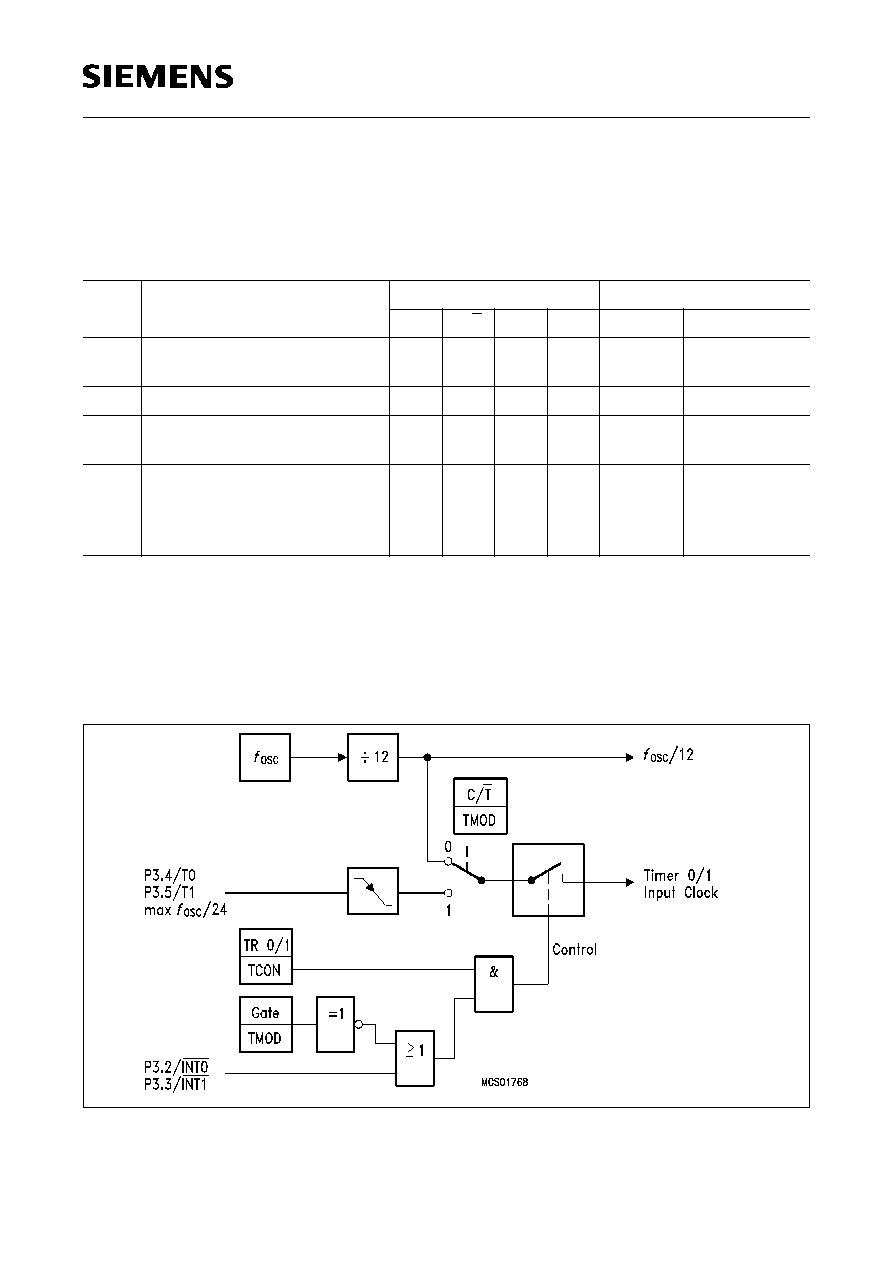
Timer/Counter 0 and 1 can be used in four operating modes as listed in table 4.
In the "timer" function (C/T = `0') the register is incremented every machine cycle. Therefore the
count rate is
f
OSC
/12.
In the "counter" function the register is incremented in response to a 1-to-0 transition at its
corresponding external input pin (P3.4/T0, P3.5/T1). Since it takes two machine cycles to detect a
falling edge the max. count rate is
f
OSC
/24. External inputs INT0 and INT1 (P3.2, P3.3) can be
programmed to function as a gate to facilitate pulse width measurements. Figure 5 illustrates the
input clock logic.
Figure 5
Timer/Counter 0 and 1 Input Clock Logic
Table 4
Timer/Counter 0 and 1 Operating Modes
Mode
Description
TMOD
Input Clock
Gate
C/T
M1
M0
internal
external (max)
0
8-bit timer/counter with a
divide-by-32 prescaler
X
X
0
0
f
OSC
/
12
◊
32
f
OSC
/
24
◊
32
1
16-bit timer/counter
X
X
1
1
f
OSC
/
12
f
OSC
/
24
2
8-bit timer/counter with
8-bit autoreload
X
X
0
0
f
OSC
/
12
f
OSC
/
24
3
Timer/counter 0 used as one
8-bit timer/counter and one
8-bit timer
Timer 1 stops
X
X
1
1
f
OSC
/
12
f
OSC
/
24
Semiconductor Group
21
C504
Timer 2
Timer 2 is a 16-bit Timer/Counter with an up/down count feature. It can operate either as timer or as
an event counter which is selected by bit C/T2 (T2CON.1). It has three operating modes as shown
in table 5.
Note:
=
falling edge
Table 5
Timer/Counter 2 Operating Modes
Mode
T2CON
T2MOD
DCEN
T2CON
EXEN
P1.1/
T2EX
Remarks
Input Clock
R
◊
CLK
or
T
◊
CLK
CP/
RL2
TR2
internal
external
(P1.0/T2)
16-bit
Auto-
reload
0
0
0
0
0
0
0
0
1
1
1
1
0
0
1
1
0
1
X
X
X
0
1
reload upon
overflow
reload trigger
(falling edge)
Down counting
Up counting
f
OSC
/12
max
f
OSC
/24
16-bit
Cap-
ture
0
0
1
1
1
1
X
X
0
1
X
16 bit Timer/
Counter (only
up-counting)
capture TH2,
TL2
RC2H,
RC2L
f
OSC
/12
max
f
OSC
/24
Baud
Rate
Gene-
rator
1
1
X
X
1
1
X
X
0
1
X
no overflow
interrupt
request (TF2)
extra external
interrupt
("Timer 2")
f
OSC
/2
max
f
OSC
/24
off
X
X
0
X
X
X
Timer 2 stops
≠
≠
C504
Semiconductor Group
22
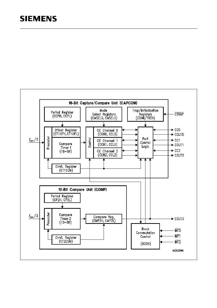
Capture/Compare Unit
The Capture / Compare Unit (CCU) of the C504 is built up by a 16-bit 3-channel capture/compare
unit (CAPCOM) and a 10-bit 1-channel compare unit (COMP). In compare mode, the CAPCOM unit
provides two output signals per channel, which can have inverted signal polarity and non-
overlapping pulse transitions. The COMP unit can generate a single PWM output signal and is
further used to modulate the CAPCOM output signals. In capture mode, the value of the compare
timer 1 is stored in the capture registers if a signal transition occurs at the pins CCx. Figure 6 shows
the block diagram of the CCU.
Figure 6
Block Diagram of the CCU

Semiconductor Group
23
C504
The compare timer 1 and 2 are free running, processor clock coupled 16-bit / 10-bit timers which
have each a count rate with a maximum of
f
OSC
/2 up to
f
OSC
/256. The compare timer operations with
its possible compare output signal waveforms are shown in figure 7.
Figure 7
Basic Operating Modes of the CAPCOM Unit
Compare timer 1 runs only in operating mode 1 with one output signal of selectable signal polarity
at the pin COUT3.
C504
Semiconductor Group
24
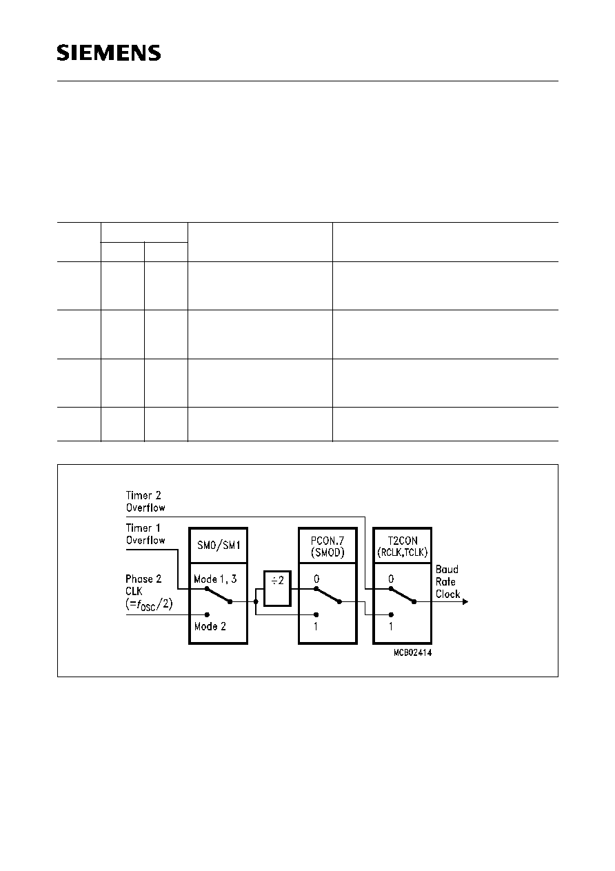
Serial Interface (USART)
The serial port is full duplex and can operate in four modes (one synchronous mode, three
asynchronous modes) as illustrated in table 6. The possible baudrates can be calculated using the
formulas given in table 6.
Figure 8
Block Diagram of Baud Rate Generation for the Serial Interface
Table 6
USART Operating Modes
Mode
SCON
Baudrate
Description
SM0
SM1
0
0
0
f
OSC
/12
Serial data enters and exits through R
◊
D.
T
◊
D outputs the shift clock. 8-bit are
transmitted/received (LSB first)
1
0
1
Timer 1/2 overflow rate
8-bit UART
10 bits are transmitted (through T
◊
D) or
received (R
◊
D)
2
1
0
f
OSC
/32 or
f
OSC
/64
9-bit UART
11 bits are transmitted (T
◊
D) or
received (R
◊
D)
3
1
1
Timer 1/2 overflow rate
9-bit UART
Like mode 2 except the variable baud rate
Semiconductor Group
25
C504
The possible baudrates can be calculated using the formulas given in table 7.
Table 7
Formulas for Calculating Baudrates
Baud Rate
derived from
Interface Mode
Baudrate
Oscillator
0
2
f
OSC
/12
(2
SMOD
◊
f
OSC
) / 64
Timer 1 (16-bit timer)
(8-bit timer with
8-bit autoreload)
1,3
1,3
(2
SMOD
◊
timer 1 overflow rate) /32
(2
SMOD
◊
f
OSC
) / (32
◊
12
◊
(256-TH1))
Timer 2
1,3
f
OSC
/ (32
◊
(65536-(RC2H, RC2L))
C504
Semiconductor Group
26
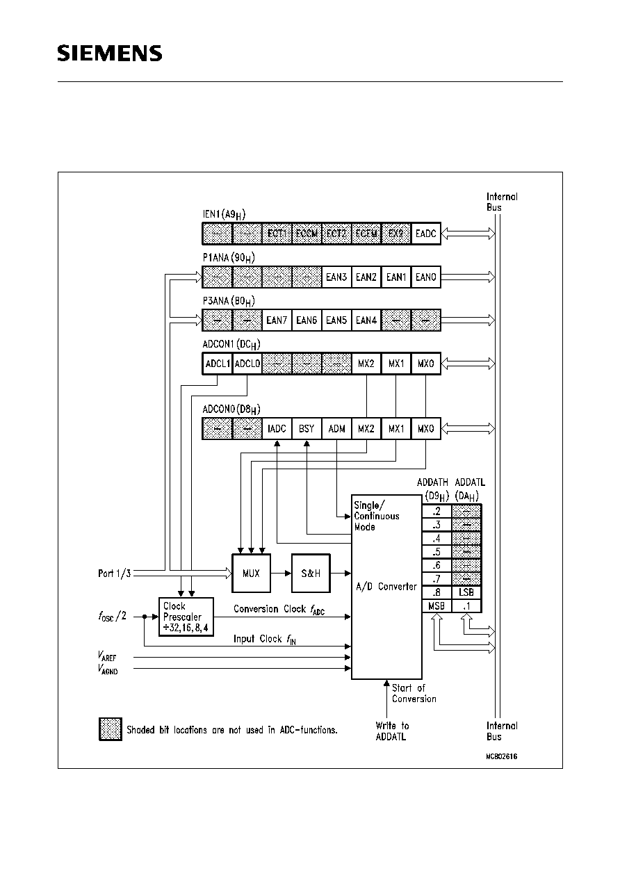
10-Bit A/D Converter
The C504 has a high performance 10-bit A/D converter (figure 9) with 8 inputs included which uses
successive approximation technique for the conversion of analog input voltages.
Figure 9
A/D Converter Block Diagram
Semiconductor Group
27
C504
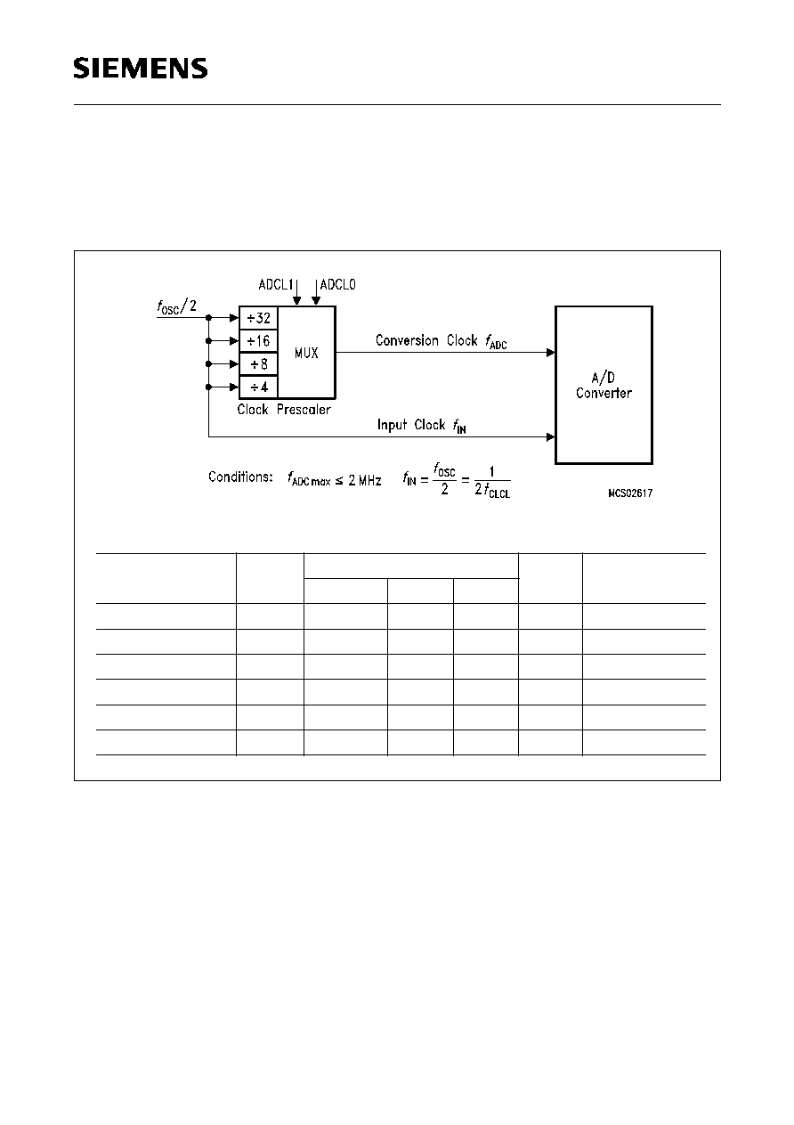
The A/D converter uses two clock signals for operation : the conversion clock f
ADC
(= 1/ t
ADC
) and
the input clock f
IN
(= 1/ t
IN
). Both clock signals are derived from the C504 system clock f
OSC
which
is applied at the XTAL pins. The duration of an A/D conversion is a multiple of the period of the f
IN
clock signal. The table in figure 10 shows the prescaler ratios and the resulting A/D conversion
times which must be selected for typical system clock rates.
Figure 10
A/D Converter Clock Selection
The analog inputs are located at port 1 and port 3 (4 lines on each port). The corresponding port 1
and port 3 pins have a port structure, which allows to use it either as digital I/Os or analog inputs.
The analog input function of these mixed digital/analog port lines is selected via the registers
P1ANA and P3ANA.
MCU System Clock
Rate (f
OSC
)
f
IN
[MHz]
Prescaler
f
ADC
[MHz]
A/D Conversion
Time [
µ
s]
Ratio
ADCL1
ADCL0
3.5 MHz
1.75
˜
4
0
0
.438
48 x t
IN
= 27.4
12 MHz
6
˜
4
0
0
1.5
48 x t
IN
= 8
16 MHz
8
˜
4
0
0
2
48 x t
IN
= 6
24 MHz
12
˜
8
0
1
1.5
96 x t
IN
= 8
32 MHz
16
˜
8
0
1
2
96 x t
IN
= 6
40 MHz
20
˜
16
1
0
1.25
192 x t
IN
= 9.6
C504
Semiconductor Group
28
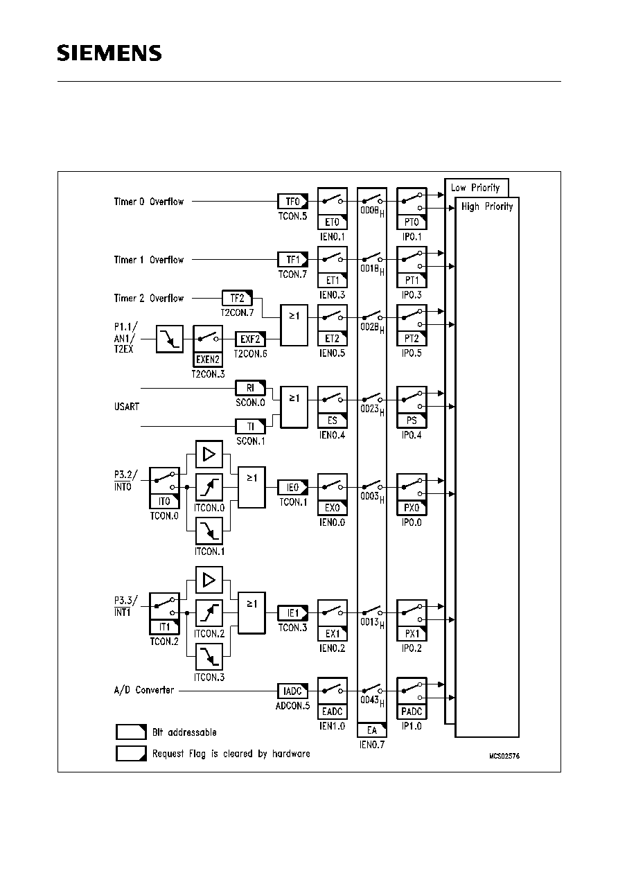
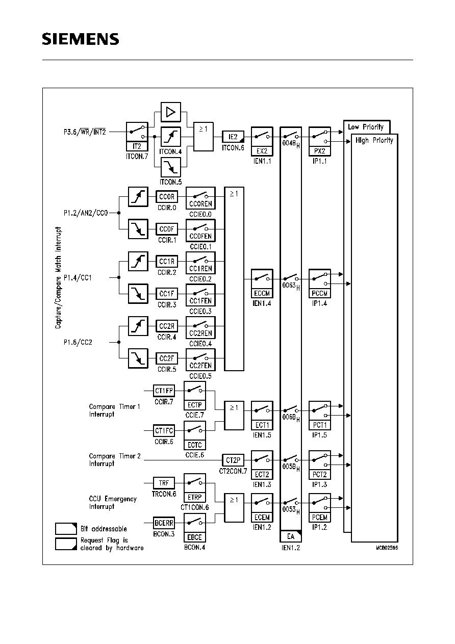
Interrupt System
The C504 provides 12 interrupt sources with two priority levels. Figure 11 and 12 give a general
overview of the interrupt sources and illustrate the interrupt request and control flags.
Figure 11
Interrupt Request Sources (Part 1)
Semiconductor Group
29
C504
Figure 12
Interrupt Request Sources (Part 2)
C504
Semiconductor Group
30
A low-priority interrupt can itself be interrupted by a high-priority interrupt, but not by another low-
priority interrupt. A high-priority interrupt cannot be interrupted by any other interrupt source.
If two requests of different priority level are received simultaneously, the request of higher priority is
serviced. If requests of the same priority are received simultaneously, an internal polling sequence
determines which request is serviced. Thus within each priority level there is a second priority
structure determined by the polling sequence as shown in table 9.
Table 8
Interrupt Vector Addresses
Request Flags
Interrupt Source
Vector Address
IE0
TF0
IE1
TF1
RI + TI
TF2 + EXF2
IADC
IE2
TRF, BCERR
CT2P
CC0F-CC2F, CC0R-CC2R
CT1FP, CT1FC
≠
External interrupt 0
Timer 0 interrupt
External interrupt 1
Timer 1 interrupt
Serial port interrupt
Timer 2 interrupt
A/D converter interrupt
External interrupt 2
CAPCOM emergency interrupt
Compare timer 2 interrupt
Capture / compare match interrupt
Compare timer 1 interrupt
Power-down interrupt
0003H
000BH
0013H
001BH
0023H
002BH
0043H
004BH
0053H
005BH
0063H
006BH
007BH
Table 9
Interrupt Source Structure
Interrupt Source
Priority
External Interrupt 0
Timer 0 Interrupt
External Interrupt 1
Timer 1 Interrupt
Serial Channel
Timer 2 Interrupt
A/D Converter
External Interrupt 2
CCU Emergency Interrupt
Compare Timer 2 Interrupt
Capture / Compare Match Interrupt
Compare Timer 1 Interrupt
High h
Low
High Priority
Low Priority
Semiconductor Group
31
C504
Fail Save Mechanisms
The C504 offers enhanced fail safe mechanisms, which allow an automatic recovery from software
upset or hardware failure.
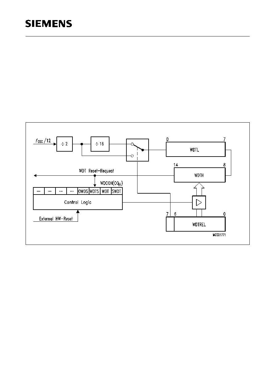
≠ 15-bit reloadable watchdog timer
≠ Oscillator Watchdog
Watchdog Timer
The watchdog timer in the C504 is a 15-bit timer, which is incremented by a count rate of either
f
SOC
/
12 or
f
CYCLE
/32. From the 15-bit watchdog timer count value only the upper 7 bits can be
programmed. Figure 5 shows the block diagram of the programmable watchdog timer.
Figure 13
Block Diagram of the Programmable Watchdog Timer
The watchdog timer can be started by software (bit SWDT in SFR WDCON), but it cannot be
stopped during active mode of the device. If the software fails to refresh the running watchdog timer
an internal reset will be initiated. The reset cause (external reset or reset caused by the watchdog)
can be examined by software (status flag WDTS in WDCON is set). A refresh of the watchdog timer
is done by setting bits WDT (SFR WDCON) and SWDT consecutively. This double instruction
sequence has been implemented to increase system security.
It must be noted, however, that the watchdog timer is halted during the idle mode and power down
mode of the processor. Therefore, it is possible to use the idle mode in combination with the
watchdog timer function.
C504
Semiconductor Group
32
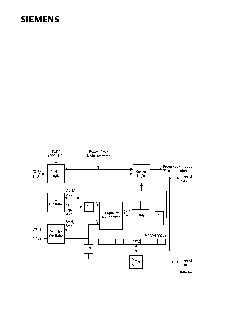
Oscillator Watchdog
The oscillator watchdog of the C504 serves for three functions :
≠ Monitoring of the on-chip oscillator's function
The watchdog supervises the on-chip oscillator's frequency; if it is lower than the frequency
of an auxiliary RC oscillator, the internal clock is supplied by this RC oscillator and the C504
is put into reset state; if the failure condition again disappears, the part executes a final reset
phase of typ. 1 ms in order to allow the oscillator to stabilize; then the oscillator watchdog reset
is released and the part starts program execution again.
≠ Fast internal reset after power-on
The oscillator watchdog unit provides a clock supply for the reset before the on-chip oscillator
has started. The oscillator watchdog unit also works identically to the monitoring function.
≠ Control of external wake-up from software power-down mode
When the power-down mode is left by a low level at the INT0 pin, the oscillator watchdog unit
assures that the microcontroller resumes operation (execution of the power-down wake-up
interrupt) with the nominal clock rate. In the power-down mode the RC oscillator and the on-
chip oscillator are stopped. Both oscillators are started again when power-down mode is
released. When the on-chip oscillator has a higher frequency than the RC oscillator, the
microcontroller starts operation after a final delay of typ. 1 ms in order to allow the on-chip
oscillator to stabilize.
Figure 14
Block Diagram of the Programmable Watchdog Timer
Semiconductor Group
33
C504
Power Saving Modes
Two power down modes are available, the idle mode and power down mode.
≠ In the idle mode the oscillator of the C504 continues to run, but the CPU is gated off from the
clock signal. However, the interrupt system, the serial port, the A/D converter, and all timers
with the exception of the watchdog timer are further provided with the clock. The CPU status
is preserved in its entirety: the stack pointer, program counter, program status word,
accumulator, and all other registers maintain their data during idle mode.
≠ In the power down mode, the RC oscillator and the on-chip oscillator which operates with the
XTAL pins is stopped. Therefore all functions of the microcontroller are stopped and only the
contents of the on-chip RAM, XRAM and the SFR's are maintained. The port pins, which are
controlled by their port latches, output the values that are held by their SFR's.
Table 10 gives a general overview of the power saving modes.
In the power down mode of operation,
V
CC
can be reduced to minimize power consumption. It must
be ensured, however, that
V
CC
is not reduced before the power down mode is invoked, and that
V
CC
is restored to its normal operating level, before the power down mode is terminated.
The idle mode can be terminated by activating any enabled peripheral interrupt or by resetting the
C504. The power down mode can be terminated using an interrupt by a short low pulse at the pin
P3.2/AN4/INT0 or by resetting the C504. If a power saving mode is left through an interrupt, the
microcontroller state (CPU, ports, peripherals) remains preserved. If a power saving mode is left by
a reset operation, the microcontroller state is disturbed and replaced by the reset state of the C504.
Table 10
Power Saving Modes Overview
Mode
Entering
2-Instruction
Example
Leaving by
Remarks
Idle mode
ORL PCON, #01H
ORL PCON, #20H
Ocurrence of an
interrupt from a
peripheral unit
CPU clock is stopped;
CPU maintains their data;
peripheral units are active (if
enabled) and provided with
clock
Hardware Reset
Power-Down
Mode
ORL PCON, #02H
ORL PCON, #40H
Hardware Reset
Oscillator is stopped;
contents of on-chip RAM and
SFR's are maintained;
Wake-up from power
down

C504
Semiconductor Group
34
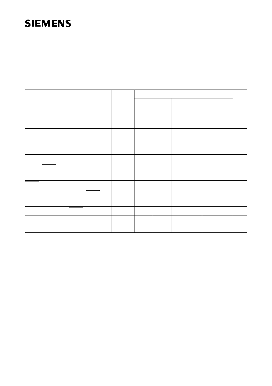
Absolute Maximum Ratings
Ambient temperature under bias (
T
A
) .............................................................. 0 ∞C to + 70 ∞C
Storage temperature (
T
ST
)................................................................................≠ 65 ∞C to + 150 ∞C
Voltage on
V
CC
pins with respect to ground (
V
SS
) ............................................≠ 0.5 V to 6.5 V
Voltage on any pin with respect to ground (
V
SS
) ..............................................≠ 0.5 V to
V
CC
+ 0.5 V
Input current on any pin during overload condition ..........................................≠ 10 mA to + 10 mA
Absolute sum of all input currents during overload condition ..........................| 100 mA |
Power dissipation.............................................................................................TBD
Note:
Stresses above those listed under "Absolute Maximum Ratings" may cause permanent
damage of the device. This is a stress rating only and functional operation of the device at
these or any other conditions above those indicated in the operational sections of this
specification is not implied. Exposure to absolute maximum rating conditions for longer
periods may affect device reliability. During overload conditions (
V
IN
>
V
CC
or
V
IN
<
V
SS
) the
Voltage on
V
CC
pins with respect to ground (
V
SS
) must not exceed the values defined by the
absolute maximum ratings.

Semiconductor Group
35
C504
DC Characteristics
V
CC
= 5 V + 10%, ≠ 15%;
V
SS
= 0 V
T
A
= 0 to 70
∞
C
for the SAB-C504
T
A
= ≠ 40 to 85
∞
C
for the SAF-C504
T
A
= ≠ 40 to 110
∞
C
for the SAH-C504
T
A
= ≠ 40 to 125
∞
C
for the SAK-C504
Parameter
Symbol
Limit Values
Unit
Test Condition
min.
max.
Input low voltage (except EA,
RESET, CTRAP)
V
IL
≠ 0.5
0.2
V
CC
≠
0.1
V
≠
Input low voltage (EA)
V
IL1
≠ 0.5
0.2
V
CC
≠
0.3
V
≠
Input low voltage (RESET,
CTRAP)
V
IL2
≠ 0.5
0.2
V
CC
+
0.1
V
≠
Input high voltage (except XTAL1,
RESET and CTRAP)
V
IH
0.2
V
CC
+
0.9
V
CC
+ 0.5
V
≠
Input high voltage to XTAL1
V
IH1
0.7
V
CC
V
CC
+ 0.5
V
≠
Input high voltage to RESET and
CTRAP
V
IH2
0.6
V
CC
V
CC
+ 0.5
V
≠
Output low voltage (ports 1, 2, 3,
COUT3)
V
OL
≠
0.45
V
I
OL
= 1.6 mA
1)
Output low voltage (port 0, ALE,
PSEN)
V
OL1
≠
0.45
V
I
OL
= 3.2 mA
1)
Output high voltage (ports 1, 2, 3)
V
OH
2.4
0.9
V
CC
≠
≠
V
I
OH
= ≠ 80
µ
A,
I
OH
= ≠ 10
µ
A
Output high voltage (ports 1,3 pins
in push-pull mode and COUT3)
V
OH1
0.9
V
CC
≠
V
I
OH
= ≠ 800
µ
A
Output high voltage (port 0 in
external bus mode, ALE, PSEN)
V
OH2
2.4
0.9
V
CC
≠
≠
V
I
OH
= ≠ 800
µ
A
2)
,
I
OH
= ≠ 80
µ
A
2)
Logic 0 input current (ports 1, 2, 3)
I
IL
≠ 10
≠ 50
µ
A
V
IN
= 0.45 V
Logical 1-to-0 transition current
(ports 1, 2, 3)
I
TL
≠ 65
≠ 650
µ
A
V
IN
= 2 V
Input leakage current (port 0, EA)
I
LI
≠
±
1
µ
A
0.45 <
V
IN
<
V
CC
Pin capacitance
C
IO
≠
10
pF
f
c
= 1 MHz,
T
A
= 25
∞
C
Overload current
I
OV
≠
±
5
mA
7) 8)
C504
Semiconductor Group
36
1) Capacitive loading on ports 0 and 2 may cause spurious noise pulses to be superimposed on the
V
OL
of ALE
and port 3. The noise is due to external bus capacitance discharging into the port 0 and port 2 pins when these
pins make 1-to-0 transitions during bus operation. In the worst case (capacitive loading > 100 pF), the noise
pulse on ALE line may exceed 0.8 V. In such cases it may be desirable to qualify ALE with a schmitt-trigger,
or use an address latch with a schmitt-trigger strobe input.
2) Capacitive loading on ports 0 and 2 may cause the
V
OH
on ALE and PSEN to momentarily fall below the
0.9
V
CC
specification when the address lines are stabilizing.
3)
I
PD
(power-down mode) is measured under following conditions:
EA = Port0 =
V
CC
; RESET =
V
SS
; XTAL2 = N.C.; XTAL1 =
V
SS
;
V
AGND
=
V
SS
; all other pins are disconnected.
4)
I
CC
(active mode) is measured with:
XTAL1 driven with
t
CLCH
,
t
CHCL
= 5 ns ,
V
IL
=
V
SS
+ 0.5 V,
V
IH
=
V
CC
≠ 0.5 V; XTAL2 = N.C.;
EA = Port0 = Port1 = RESET =
V
CC
; all other pins are disconnected.
I
CC
would be slightly higher if a crystal
oscillator is used (appr. 1 mA).
5)
I
CC
(idle mode) is measured with all output pins disconnected and with all peripherals disabled;
XTAL1 driven with
t
CLCH
,
t
CHCL
= 5 ns,
V
IL
=
V
SS
+ 0.5 V,
V
IH
=
V
CC
≠ 0.5 V; XTAL2 = N.C.;
RESET = EA =
V
SS
; Port0 =
V
CC
; all other pins are disconnected.
6)
I
CC max
at other frequencies is given by:
active mode:
TBD
idle mode:
TBD
where
f
osc
is the oscillator frequency in MHz.
I
CC
values are given in mA and measured at
V
CC
= 5 V.
7) Overload conditions occur if the standard operating conditions are exceeded, i.e. the voltage on any pin
exceeds the specified range (i.e.
V
OV
>
V
CC
+ 0.5 V or
V
OV
<
V
SS
≠
0.5 V). The supply voltage
V
CC
and
V
SS
must remain within the specified limits. The absolute sum of input currents on all port pins may not exceed 50
mA.
8) Not 100 % tested, guaranteed by design characterization.
9) The typical
I
CC
values are periodically measured at
T
A
= +25 ∞C but not 100% tested.
Parameter
Symbol
Limit Values
Unit Test Condition
typ.
9)
max.
Power supply current:
Active mode, 12 MHz
4)
Idle mode, 12 MHz
5)
Active mode, 24 MHz
4)
Idle mode, 24 MHz
5)
Active mode, 40 MHz
4)
Idle mode, 40 MHz
5)
Power-down mode
I
CC
I
CC
I
CC
I
CC
I
CC
I
CC
I
PD
16
8
25
13
38
17
1
TBD
TBD
TBD
TBD
TBD
TBD
50
mA
mA
mA
mA
mA
mA
µ
A
V
CC
= 5 V,
4)
V
CC
= 5 V,
5)
V
CC
= 5 V,
4)
V
CC
= 5 V,
5)
V
CC
= 5 V,
4)
V
CC
= 5 V,
5)
V
CC
= 2
...
5.5 V
3)

Semiconductor Group
37
C504
A/D Converter Characteristics
V
CC
= 5 V + 10%, ≠ 15%;
V
SS
= 0 V
T
A
= 0 to 70
∞
C
for the SAB-C504
4V
V
AREF
V
CC
+ 0.1 V;
T
A
= ≠ 40 to 85
∞
C
for the SAF-C504
V
SS
≠ 0.1 V
V
AGND
V
SS
+ 0.2 V;
T
A
= ≠ 40 to 110
∞
C
for the SAH-C504
T
A
= ≠ 40 to 125
∞
C
for the SAK-C504
Notes see next page.
Clock calculation table :
Further timing conditions : t
ADC
min = 500 ns
t
IN
= 2 / f
OSC
= 2 t
CLCL
Parameter
Symbol
Limit Values
Unit
Test Condition
min.
max.
Analog input voltage
V
AIN
V
AGND
V
AREF
V
1)
Sample time
t
S
≠
64 x
t
IN
32 x
t
IN
16 x
t
IN
8 x
t
IN
ns
Prescaler
˜
32
Prescaler
˜
16
Prescaler
˜
8
Prescaler
˜
4
2)
Conversion cycle time
t
ADCC
≠
384 x
t
IN
192 x
t
IN
96 x
t
IN
48 x
t
IN
ns
Prescaler
˜
32
Prescaler
˜
16
Prescaler
˜
8
Prescaler
˜
4
3)
Total unadjusted error
T
UE
≠
±
2
LSB
V
SS
+ 0.5V
V
IN
V
CC
≠ 0.5V
4)
≠
±
4
LSB
V
SS
< V
IN
< V
SS
+ 0.5V
V
CC
≠ 0.5V < V
IN
< V
CC
4)
Internal resistance of
reference voltage source
R
AREF
≠
t
ADC
/ 250
≠ 0.25
k
t
ADC
in [ns]
5) 6)
Internal resistance of
analog source
R
ASRC
≠
t
S
/ 500
≠ 0.25
k
t
S
in [ns]
2) 6)
ADC input capacitance
C
AIN
≠
50
pF
6)
Clock Prescaler
Ratio
ADCL1, 0
t
ADC
t
S
t
ADCC
˜
32
1 1
32 x t
IN
64 x t
IN
384 x t
IN
˜
16
1 0
16 x t
IN
32 x t
IN
192 x t
IN
˜
8
0 1
8 x t
IN
16 x t
IN
96 x t
IN
˜
4
0 0
4 x t
IN
8 x t
IN
48 x t
IN

C504
Semiconductor Group
38
Notes:
1) V
AIN
may exceed V
AGND
or V
AREF
up to the absolute maximum ratings. However, the conversion result in
these cases will be X000
H
or X3FF
H
, respectively.
2) During the sample time the input capacitance
C
AIN
can be charged/discharged by the external source. The
internal resistance of the analog source must allow the capacitance to reach their final voltage level within t
S
.
After the end of the sample time t
S
, changes of the analog input voltage have no effect on the conversion
result.
3) This parameter includes the sample time t
S
, the time for determining the digital result and the time for the
calibration. Values for the conversion clock t
ADC
depend on programming and can be taken from the table on
the previous page.
4) T
UE
is tested at V
AREF
= 5.0 V, V
AGND
= 0 V, V
CC
= 4.9 V. It is guaranteed by design characterization for all
other voltages within the defined voltage range.
If an overload condition occurs on maximum 2 not selected analog input pins and the absolute sum of input
overload currents on all analog input pins does not exceed 10 mA, an additional conversion error of 1/2 LSB
is permissible.
5) During the conversion the ADC's capacitance must be repeatedly charged or discharged. The internal
resistance of the reference source must allow the capacitance to reach their final voltage level within the
indicated time. The maximum internal resistance results from the programmed conversion timing.
6) Not 100 % tested, but guaranteed by design characterization.

Semiconductor Group
39
C504
AC Characteristics for C504-L / C504-2R
V
CC
= 5 V + 10%, ≠ 15%;
V
SS
= 0 V
T
A
= 0 to 70
∞
C
for the SAB-C504
T
A
= ≠ 40 to 85
∞
C
for the SAF-C504
T
A
= ≠ 40 to 110
∞
C
for the SAH-C504
T
A
= ≠ 40 to 125
∞
C
for the SAK-C504
(
C
L
for port 0, ALE and PSEN outputs = 100 pF;
C
L
for all other outputs = 80 pF)
Program Memory Characteristics
*)
Interfacing the C504 to devices with float times up to 75 ns is permissible. This limited bus contention will not
cause any damage to port 0 drivers.
Parameter
Symbol
Limit Values
Unit
12-MHz clock
Variable Clock
1/
t
CLCL
= 3.5 MHz to
12 MHz
min.
max.
min.
max.
ALE pulse width
t
LHLL
127
≠
2
t
CLCL
≠ 40
≠
ns
Address setup to ALE
t
AVLL
43
≠
t
CLCL
≠ 40
≠
ns
Address hold after ALE
t
LLAX
30
≠
t
CLCL
≠ 23
≠
ns
ALE low to valid instr in
t
LLIV
≠
233
≠
4
t
CLCL
≠ 100 ns
ALE to PSEN
t
LLPL
58
≠
t
CLCL
≠ 25
≠
ns
PSEN pulse width
t
PLPH
215
≠
3
t
CLCL
≠ 35
≠
ns
PSEN to valid instr in
t
PLIV
≠
150
≠
3
t
CLCL
≠ 100 ns
Input instruction hold after PSEN
t
PXIX
0
≠
0
≠
ns
Input instruction float after PSEN
t
PXIZ
*)
≠
63
≠
t
CLCL
≠ 20
ns
Address valid after PSEN
t
PXAV
*)
75
≠
t
CLCL
≠ 8
≠
ns
Address to valid instr in
t
AVIV
≠
302
≠
5
t
CLCL
≠ 115 ns
Address float to PSEN
t
AZPL
0
≠
0
≠
ns

C504
Semiconductor Group
40
AC Characteristics for C504-L / C504-2R (cont'd)
External Data Memory Characteristics
External Clock Drive
Parameter
Symbol
Limit Values
Unit
12-MHz clock
Variable Clock
1/
t
CLCL
= 3.5 MHz to
12 MHz
min.
max.
min.
max.
RD pulse width
t
RLRH
400
≠
6
t
CLCL
≠ 100 ≠
ns
WR pulse width
t
WLWH
400
≠
6
t
CLCL
≠ 100 ≠
ns
Address hold after ALE
t
LLAX2
114
≠
2
t
CLCL
≠ 53
≠
ns
RD to valid data in
t
RLDV
≠
252
≠
5
t
CLCL
≠ 165 ns
Data hold after RD
t
RHDX
0
≠
0
≠
ns
Data float after RD
t
RHDZ
≠
97
≠
2
t
CLCL
≠ 70
ns
ALE to valid data in
t
LLDV
≠
517
≠
8
t
CLCL
≠ 150 ns
Address to valid data in
t
AVDV
≠
585
≠
9
t
CLCL
≠ 165 ns
ALE to WR or RD
t
LLWL
200
300
3
t
CLCL
≠ 50
3
t
CLCL
+ 50
ns
Address valid to WR or RD
t
AVWL
203
≠
4
t
CLCL
≠ 130 ≠
ns
WR or RD high to ALE high
t
WHLH
43
123
t
CLCL
≠ 40
t
CLCL
+ 40
ns
Data valid to WR transition
t
QVWX
33
≠
t
CLCL
≠ 50
≠
ns
Data setup before WR
t
QVWH
433
≠
7
t
CLCL
≠ 150 ≠
ns
Data hold after WR
t
WHQX
33
≠
t
CLCL
≠ 50
≠
ns
Address float after RD
t
RLAZ
≠
0
≠
0
ns
Parameter
Symbol
Limit Values
Unit
Variable Clock
Freq. = 3.5 MHz to 12 MHz
min.
max.
Oscillator period
t
CLCL
83.3
294
ns
High time
t
CHCX
20
t
CLCL
≠
t
CLCX
ns
Low time
t
CLCX
20
t
CLCL
≠
t
CHCX
ns
Rise time
t
CLCH
≠
20
ns
Fall time
t
CHCL
≠
20
ns
Semiconductor Group
41
C504
AC Characteristics for C504-L24 / C504-2R24
V
CC
= 5 V + 10 %, ≠ 15 %;
V
SS
= 0 V
T
A
= 0 to 70
∞
C
for the SAB-C504
T
A
= ≠ 40 to 85
∞
C
for the SAF-C504
(
C
L
for port 0, ALE and PSEN outputs = 100 pF;
C
L
for all other outputs = 80 pF)
Program Memory Characteristics
*)
Interfacing the C504 to devices with float times up to 37 ns is permissible. This limited bus contention will not
cause any damage to port 0 drivers.
Parameter
Symbol
Limit Values
Unit
24-MHz clock
Variable Clock
1/
t
CLCL
= 3.5 MHz to
24 MHz
min.
max.
min.
max.
ALE pulse width
t
LHLL
43
≠
2
t
CLCL
≠ 40
≠
ns
Address setup to ALE
t
AVLL
17
≠
t
CLCL
≠ 25
≠
ns
Address hold after ALE
t
LLAX
17
≠
t
CLCL
≠ 25
≠
ns
ALE low to valid instr in
t
LLIV
≠
80
≠
4
t
CLCL
≠ 87
ns
ALE to PSEN
t
LLPL
22
≠
t
CLCL
≠ 20
≠
ns
PSEN pulse width
t
PLPH
95
≠
3
t
CLCL
≠ 30
≠
ns
PSEN to valid instr in
t
PLIV
≠
60
≠
3
t
CLCL
≠ 65
ns
Input instruction hold after PSEN
t
PXIX
0
≠
0
≠
ns
Input instruction float after PSEN
t
PXIZ
*)
≠
32
≠
t
CLCL
≠ 10
ns
Address valid after PSEN
t
PXAV
*)
37
≠
t
CLCL
≠ 5
≠
ns
Address to valid instr in
t
AVIV
≠
148
≠
5
t
CLCL
≠ 60
ns
Address float to PSEN
t
AZPL
0
≠
0
≠
ns
C504
Semiconductor Group
42
AC Characteristics for C504-L24 / C504-2R24 (cont'd)
External Data Memory Characteristics
External Clock Drive
Parameter
Symbol
Limit Values
Unit
24-MHz clock
Variable Clock
1/
t
CLCL
= 3.5 MHz to
24 MHz
min.
max.
min.
max.
RD pulse width
t
RLRH
180
≠
6
t
CLCL
≠ 70
≠
ns
WR pulse width
t
WLWH
180
≠
6
t
CLCL
≠ 70
≠
ns
Address hold after ALE
t
LLAX2
56
≠
2
t
CLCL
≠ 27
≠
ns
RD to valid data in
t
RLDV
≠
118
≠
5
t
CLCL
≠ 90
ns
Data hold after RD
t
RHDX
0
0
≠
ns
Data float after RD
t
RHDZ
≠
63
≠
2
t
CLCL
≠ 20
ns
ALE to valid data in
t
LLDV
≠
200
≠
8
t
CLCL
≠ 133 ns
Address to valid data in
t
AVDV
≠
220
≠
9
t
CLCL
≠ 155 ns
ALE to WR or RD
t
LLWL
75
175
3
t
CLCL
≠ 50
3
t
CLCL
+ 50
ns
Address valid to WR
t
AVWL
67
≠
4
t
CLCL
≠ 97
≠
ns
WR or RD high to ALE high
t
WHLH
17
67
t
CLCL
≠ 25
t
CLCL
+ 25
ns
Data valid to WR transition
t
QVWX
5
≠
t
CLCL
≠ 37
≠
ns
Data setup before WR
t
QVWH
170
≠
7
t
CLCL
≠ 122 ≠
ns
Data hold after WR
t
WHQX
15
≠
t
CLCL
≠ 27
≠
ns
Address float after RD
t
RLAZ
≠
0
≠
0
ns
Parameter
Symbol
Limit Values
Unit
Variable Clock
Freq. = 3.5 MHz to 24 MHz
min.
max.
Oscillator period
t
CLCL
41.7
294
ns
High time
t
CHCX
12
t
CLCL
≠
t
CLCX
ns
Low time
t
CLCX
12
t
CLCL
≠
t
CHCX
ns
Rise time
t
CLCH
≠
12
ns
Fall time
t
CHCL
≠
12
ns
Semiconductor Group
43
C504
AC Characteristics for C504-L40 / C504-2R40
V
CC
= 5 V + 10 %, ≠ 15 %;
V
SS
= 0 V
T
A
= 0 to 70
∞
C
for the SAB-C504
T
A
= ≠ 40 to 85
∞
C
for the SAF-C504
(
C
L
for port 0, ALE and PSEN outputs = 100 pF;
C
L
for all other outputs = 80 pF)
Program Memory Characteristics
*)
Interfacing the C504 to devices with float times up to 25 ns is permissible. This limited bus contention will not
cause any damage to port 0 drivers.
Parameter
Symbol
Limit Values
Unit
40-MHz clock
Variable Clock
1/
t
CLCL
= 3.5 MHz to
40 MHz
min.
max.
min.
max.
ALE pulse width
t
LHLL
35
≠
2
t
CLCL
≠ 15
≠
ns
Address setup to ALE
t
AVLL
10
≠
t
CLCL
≠ 15
≠
ns
Address hold after ALE
t
LLAX
10
≠
t
CLCL
≠ 15
≠
ns
ALE low to valid instr in
t
LLIV
≠
55
≠
4
t
CLCL
≠ 45
ns
ALE to PSEN
t
LLPL
10
≠
t
CLCL
≠ 15
≠
ns
PSEN pulse width
t
PLPH
60
≠
3
t
CLCL
≠ 15
≠
ns
PSEN to valid instr in
t
PLIV
≠
25
≠
3
t
CLCL
≠ 50
ns
Input instruction hold after PSEN
t
PXIX
0
≠
0
≠
ns
Input instruction float after PSEN
t
PXIZ
*)
≠
20
≠
t
CLCL
≠ 5
ns
Address valid after PSEN
t
PXAV
*)
20
≠
t
CLCL
≠ 5
≠
ns
Address to valid instr in
t
AVIV
≠
65
≠
5
t
CLCL
≠ 60
ns
Address float to PSEN
t
AZPL
≠ 5
≠
≠ 5
≠
ns

C504
Semiconductor Group
44
AC Characteristics for C504-L40 / C504-2R40 (cont'd)
External Data Memory Characteristics
External Clock Drive
Parameter
Symbol
Limit Values
Unit
40-MHz clock
Variable Clock
1/
t
CLCL
= 3.5 MHz to
40 MHz
min.
max.
min.
max.
RD pulse width
t
RLRH
120
≠
6
t
CLCL
≠ 30
≠
ns
WR pulse width
t
WLWH
120
≠
6
t
CLCL
≠ 30
≠
ns
Address hold after ALE
t
LLAX2
35
≠
2
t
CLCL
≠ 15
≠
ns
RD to valid data in
t
RLDV
≠
75
≠
5
t
CLCL
≠ 50
ns
Data hold after RD
t
RHDX
0
0
≠
ns
Data float after RD
t
RHDZ
≠
38
≠
2
t
CLCL
≠ 12
ns
ALE to valid data in
t
LLDV
≠
150
≠
8
t
CLCL
≠ 50
ns
Address to valid data in
t
AVDV
≠
150
≠
9
t
CLCL
≠ 75
ns
ALE to WR or RD
t
LLWL
60
90
3
t
CLCL
≠ 15
3
t
CLCL
+ 15
ns
Address valid to WR
t
AVWL
70
≠
4
t
CLCL
≠ 30
≠
ns
WR or RD high to ALE high
t
WHLH
10
40
t
CLCL
≠ 15
t
CLCL
+ 15
ns
Data valid to WR transition
t
QVWX
5
≠
t
CLCL
≠ 20
≠
ns
Data setup before WR
t
QVWH
125
≠
7
t
CLCL
≠ 50
≠
ns
Data hold after WR
t
WHQX
5
≠
t
CLCL
≠ 20
≠
ns
Address float after RD
t
RLAZ
≠
0
≠
0
ns
Parameter
Symbol
Limit Values
Unit
Variable Clock
Freq. = 3.5 MHz to 40 MHz
min.
max.
Oscillator period
t
CLCL
25
294
ns
High time
t
CHCX
10
t
CLCL
≠
t
CLCX
ns
Low time
t
CLCX
10
t
CLCL
≠
t
CHCX
ns
Rise time
t
CLCH
≠
10
ns
Fall time
t
CHCL
≠
10
ns
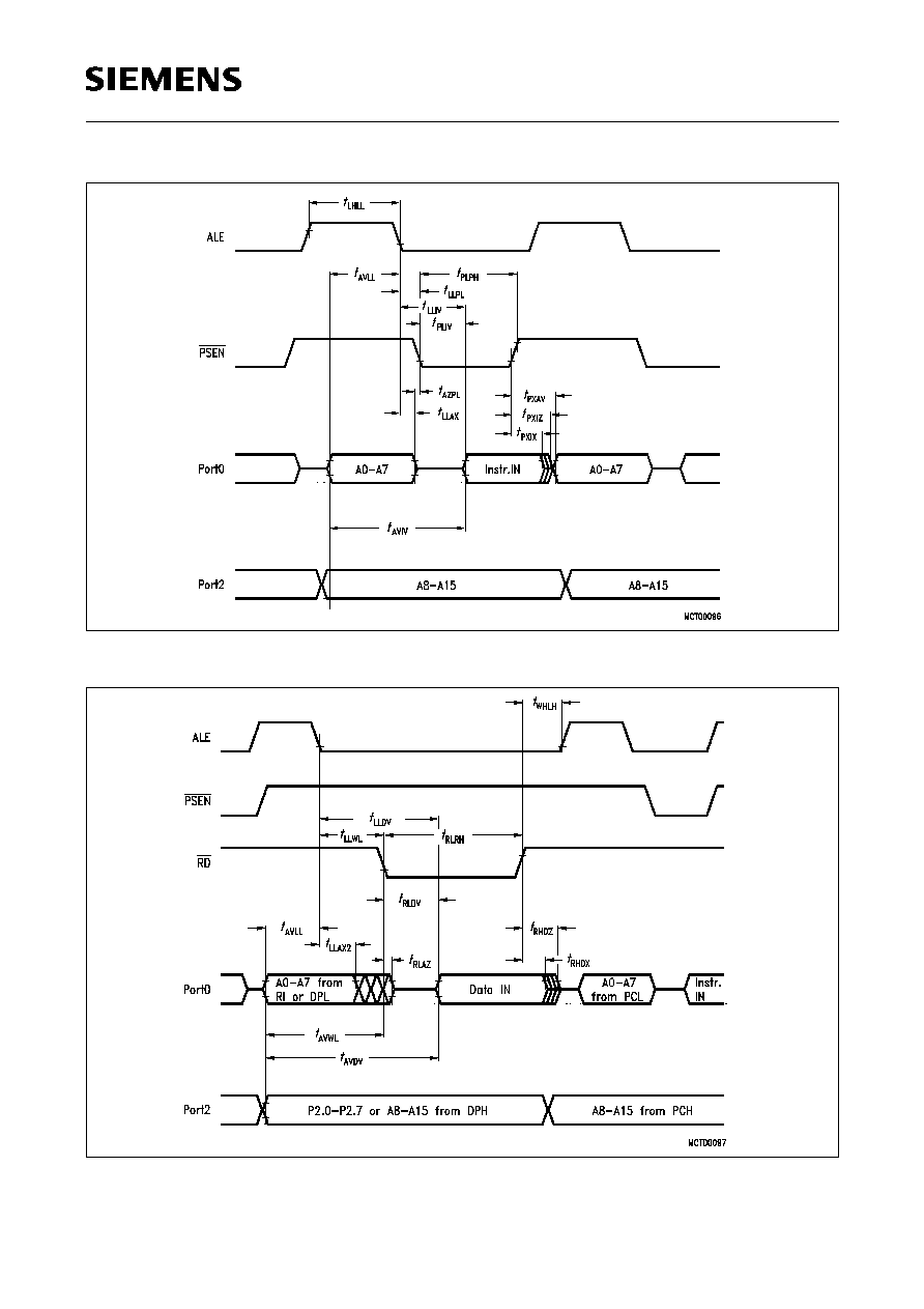
Semiconductor Group
45
C504
Figure 15
Program Memory Read Cycle
Figure 16
Data Memory Read Cycle
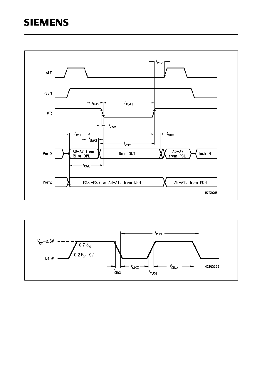
C504
Semiconductor Group
46
Figure 17
Data Memory Write Cycle
Figure 18
External Clock Cycle

Semiconductor Group
47
C504
ROM Verification Characteristics for C504-2R
ROM Verification Mode 1
Figure 19
ROM Verification Mode 1
Parameter
Symbol
Limit Values
Unit
min.
max.
Address to valid data
t
AVQV
≠
48
t
CLCL
ns
ENABLE to valid data
t
ELQV
≠
48
t
CLCL
ns
Data float after ENABLE
t
EHQZ
0
48
t
CLCL
ns
Oscillator frequency
1/
t
CLCL
4
6
MHz

C504
Semiconductor Group
48
ROM Verification Mode 2
Figure 20
ROM Verification Mode 2
Parameter
Symbol
Limit Values
Unit
min.
typ
max.
ALE pulse width
t
AWD
≠
2
t
CLCL
≠
ns
ALE period
t
ACY
≠
12
t
CLCL
≠
ns
Data valid after ALE
t
DVA
≠
≠
4
t
CLCL
ns
Data stable after ALE
t
DSA
8
t
CLCL
≠
≠
ns
P3.5 setup to ALE low
t
AS
≠
t
CLCL
≠
ns
Oscillator frequency
1/
t
CLCL
4
≠
6
MHz

Semiconductor Group
49
C504
Figure 21
AC Testing: Input, Output Waveforms
Figure 22
AC Testing : Float Waveforms
Figure 23
Recommended Oscillator Circuits for Crystal Oscillator
AC Inputs during testing are driven at
V
CC
≠ 0.5 V for a logic '1' and 0.45 V for a logic '0'.
Timing measurements are made at
V
IHmin
for a logic '1' and
V
ILmax
for a logic '0'.
For timing purposes a port pin is no longer floating when a 100 mV change from load voltage
occurs and begins to float when a 100 mV change from the loaded
V
OH
/
V
OL
level occurs.
I
OL
/
I
OH
±
20 mA