
Data Sheet 12.97
Microcomputer Components
C505
C505C/C505A
C505CA
8-Bit CMOS Microcontroller

Edition 12.97
Published by
Siemens AG,
Bereich Halbleiter, Marketing-
Kommunikation, Balanstraþe 73,
81541 M¸nchen
©
Siemens AG 1997.
All Rights Reserved.
Attention please!
As far as patents or other rights of third parties are concerned, liability is only assumed for components, not for applications, processes
and circuits implemented within components or assemblies.
The information describes the type of component and shall not be considered as assured characteristics.
Terms of delivery and rights to change design reserved.
For questions on technology, delivery and prices please contact the Semiconductor Group Offices in Germany or the Siemens Companies
and Representatives worldwide (see address list).
Due to technical requirements components may contain dangerous substances. For information on the types in question please contact
your nearest Siemens Office, Semiconductor Group.
Siemens AG is an approved CECC manufacturer.
Packing
Please use the recycling operators known to you. We can also help you ≠ get in touch with your nearest sales office. By agreement we
will take packing material back, if it is sorted. You must bear the costs of transport.
For packing material that is returned to us unsorted or which we are not obliged to accept, we shall have to invoice you for any costs in-
curred.
Components used in life-support devices or systems must be expressly authorized for such purpose!
Critical components
1
of the Semiconductor Group of Siemens AG, may only be used in life-support devices or systems
2
with the express
written approval of the Semiconductor Group of Siemens AG.
1 A critical component is a component used in a life-support device or system whose failure can reasonably be expected to cause the
failure of that life-support device or system, or to affect its safety or effectiveness of that device or system.
2 Life support devices or systems are intended (a) to be implanted in the human body, or (b) to support and/or maintain and sustain hu-
man life. If they fail, it is reasonable to assume that the health of the user may be endangered.
Semiconductor Group
3
1997-12-01
8-Bit CMOS Microcontroller
Advance Information
∑ Fully compatible to standard 8051 microcontroller
∑ Superset of the 8051 architecture with 8 datapointers
∑ Up to 20 MHz operating frequency
≠ 375 ns instruction cycle time @16 MHz
≠ 300 ns instruction cycle time @20 MHz (50 % duty cycle)
∑ On-chip program memory (with optional memory protection)
≠ C505-2R/C505C-2R :
16k byte on-chip ROM
≠ C505A-4E/C505CA-4E:
32k byte on-chip OTP
≠ alternatively up to 64k byte external program memory
∑ 256 byte on-chip RAM
∑ On-chip XRAM
≠ C505/C505C :
256 byte
≠ C505A/C505CA :
1K byte
∑ 32 + 2 digital I/O lines
≠ Four 8-bit digital I/O ports
≠ One 2-bit digital I/O port (port 4)
≠ Port 1 with mixed analog/digital I/O capability
(more features on next page)
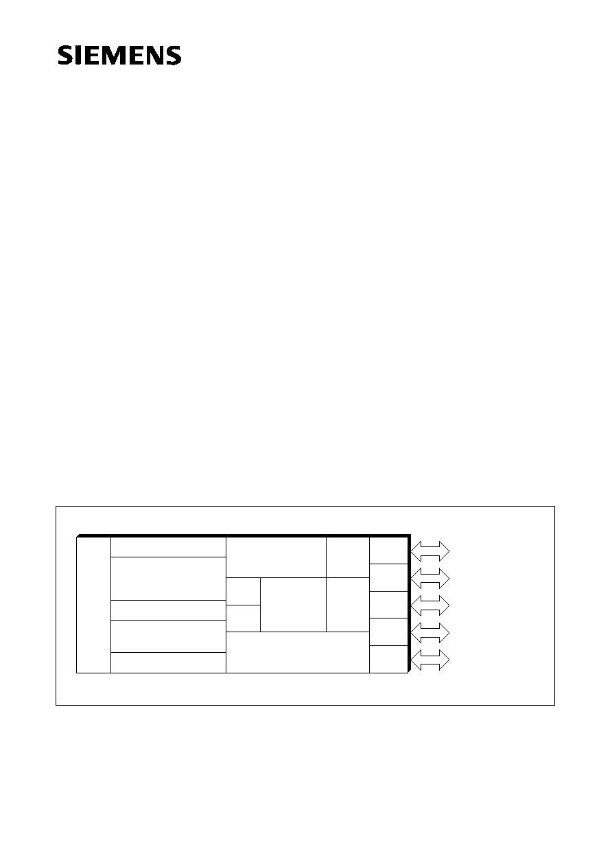
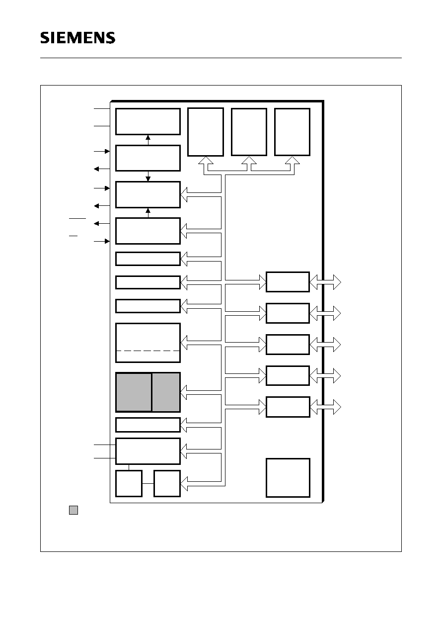
Figure 1
C505 Functional Units
I / O
8 Analog Inputs /
MCB03628
On-Chip Emulation
Port 4
Port 3
Port 2
Port 1
Port 0
8 Digit. I / O
I / O
I / O
I / O (2-Bit I / O Port)
Support Module
Timer 2
A / D Converter
C505C / C505CA only
Full-CAN Controller
Core
8 Datapointers
Program Memory
XRAM
256 Byte
RAM
8-Bit
USART
Watchdog Timer
Oscillator Watchdog
C505 / C505C: 8-Bit
C505A / C505CA: 10-Bit
C500
C505A / C505CA: 1 KByte
C505 / C505C: 256 Byte
Timer
0
1
Timer
C505A / C505CA: 32 k OTP
C505 / C505C: 16 k ROM
C505
C505C
C505A
C505CA

Semiconductor Group
4
1997-12-01
C505 / C505C
C505A / C505CA
Features
(cont'd):
∑ Three 16-bit timers/counters
≠ Timer 0 / 1 (C501 compatible)
≠ Timer 2 with 4 channels for 16-bit capture/compare operation
∑ Full duplex serial interface with programmable baudrate generator (USART)
∑ Full CAN Module, version 2.0 B compliant (C505C and C505CA only)
≠ 256 register/data bytes located in external data memory area
≠ 1 MBaud CAN baudrate when operating frequency is equal to or above 8 MHz
≠ internal CAN clock prescaler when input frequency is over 10 MHz
∑ On-chip A/D Converter
≠ up to 8 analog inputs
≠ C505/C505C
: 8-bit resolution
≠ C505A/C505CA: 10-bit resolution
∑ Twelve interrupt sources with four priority levels
∑
On-chip emulation support logic (Enhanced Hooks Technology
TM
1)
)
∑ Programmable 15-bit watchdog timer
∑ Oscillator watchdog
∑ Fast power on reset
∑ Power Saving Modes
≠ Slow-down mode
≠ Idle mode (can be combined with slow-down mode)
≠ Software power-down mode with wake up capability through P3.2/INT0 or P4.1/RXDC pin
∑ P-MQFP-44 package
∑ Pin configuration is compatible to C501, C504, C511/C513-family
∑ Temperature ranges:
SAB-C505 versions
T
A
= 0 to 70
∞
C
SAF-C505 versions
T
A
= ≠ 40 to 85
∞
C
SAH-C505 versions
T
A
= ≠ 40 to 110
∞
C (max. operating frequency: TBD)
SAK-C505 versions
T
A
= ≠ 40 to 125
∞
C (max. operating frequency: 12 MHz
with 50% duty cycle)
1)
"Enhanced Hooks Technology" is a trademark and patent of Metalink Corporation licensed to Siemens.
Table 1
Differences in Functionality of the C505 MCUs
Device
Internal Program Memory XRAM Size
A/D Converter
Resolution
CAN
Controller
ROM
OTP
C505-2RM
C505-LM
16 KB
≠
≠
≠
256 B
256 B
8 Bit
8 Bit
≠
≠
C505C-2RM
C505C-LM
16 KB
≠
≠
≠
256 B
256 B
8 Bit
8 Bit
C505A-4EM
≠
32 KB
1 KB
10 Bit
≠
C505CA-4EM
≠
32 KB
1 KB
10 Bit
Semiconductor Group
5
1997-12-01
C505 / C505C
C505A / C505CA
Note:
The ordering number of the ROM types (DXXXX extension) is defined after program release
(verification) of the customer.
Versions for the extended temperature range ≠ 40
∞
C to 110
∞
C (SAH-C505) and ≠ 40
∞
C to
125
∞
C (SAK-C505) are available on request.
Table 2
Ordering Information
Type
Ordering Code Package
Description
(8-Bit CMOS microcontroller)
SAB-C505-2RM
SAB-C505-LM
Q67127-DXXXX
Q67127-C2057
P-MQFP-44
P-MQFP-44
with mask-programmable ROM (16K), 20 MHz
for external memory (20 MHz)
SAF-C505-2RM
SAF-C505-LM
Q67127-DXXXX
Q67127-C2056
P-MQFP-44
P-MQFP-44
Extended temperature. ≠ 40
∞
C to 85
∞
C :
with mask-programmable ROM (16K), 20 MHz
for external memory (20 MHz)
SAB-C505C-2RM
SAB-C505C-LM
Q67127-DXXXX
Q67127-C2029
P-MQFP-44
P-MQFP-44
with mask-progr. ROM (16K) and CAN, 20 MHz
for external memory, with CAN (20 MHz)
SAF-C505C-2RM
SAF-C505C-LM
Q67127-DXXXX
Q67127-C2030
P-MQFP-44
P-MQFP-44
Extended temperature. ≠ 40
∞
C to 85
∞
C :
with mask-progr. ROM (16K) and CAN, 20 MHz
for external memory, with CAN (20 MHz)
SAB-C505A-4EM
Q67127-C2060
P-MQFP-44 with OTP memory (32K), 20 MHz
SAF-C505A-4EM
Q67127-C2061
P-MQFP-44
Extended temperature. ≠ 40
∞
C to 85
∞
C :
with OTP memory (32K), 20 MHz
SAB-C505CA-4EM
Q67127-C1082
P-MQFP-44 with OTP memory (32K) and CAN, 20 MHz
SAB-C505CA-4EM
Q67127-C2058
P-MQFP-44
Extended temperature. ≠ 40
∞
C to 85
∞
C :
with OTP memory (32K) and CAN, 20 MHz
Semiconductor Group
6
1997-12-01
C505 / C505C
C505A / C505CA
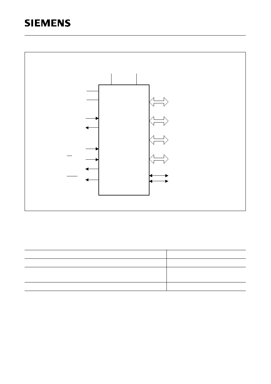
Figure 2
Logic Symbol
Additional Literature
For further information about the C505/C505C/C505A/C505CA the following literature is available:
Title
Ordering Number
C505 8-Bit CMOS Microcontroller User's Manual
B158-H7116-X-X-7600
C500 Microcontroller Family
Architecture and Instruction Set User's Manual
B158-H6987-X-X-7600
C500 Microcontroller Family - Pocket Guide
B158-H6986-X-X-7600
AGND
AREF
V
V
EA
PSEN
RESET
ALE
XTAL2
XTAL1
2-Bit Digital I / O
8-Bit Digital I / O
8-Bit Digital I / O
Port 4
Port
2
3
Port
Port
8-Bit Digital I / O /
8-Bit Digital I / O
1
Port
0
Port
V
SS
V
CC
C505
MCL03629
8-Bit Analog Inputs
C505C
C505CA
C505A
Semiconductor Group
7
1997-12-01
C505 / C505C
C505A / C505CA
Figure 3
C505 Pin Configuration P-MQFP-44 Package
(top view)
EA
P0.6 / AD6
P0.7 / AD7
P0.5 / AD5
P2.6 / A14
P2.5 / A13
PSEN
P2.7 / A15
ALE
P2.4 / A12
P2.3 / A11
XTAL2
XTAL1
P1.7 / AN7 / T2
P3.2 / INT0
P3.3 / INT1
RESET
P1.6 / AN6 / CLKOUT
P1.5 / AN5 / T2EX
11
1
6
34
39
44
16
21
22
C505
MCP03630
P2.2 / A10
P2.1 / A9
V
V
CC
SS
P2.0 / A8
33
31 30 29 28 27 26 25 24 23
32
P0.4 / AD4
P3.0 / RxD
P3.4 / T0
P3.5 / / T1
P3.1 / TxD
P1.4 / AN4
V
V
AREF
AGND
2 3 4 5
7 8
10
9
20
19
18
17
15
14
13
12
43
42
41
40
38
37
36
35
C505C
P1.1 / AN1 / INT4 / CC1
P1.0 / AN0 / INT3 / CC0
P1.3 / AN3 / INT6 / CC3
P1.2 / AN2 / INT5 / CC2
P0.3 / AD3
P0.2 / AD2
P0.1 / AD1
P0.0 / AD0
P3.7 / RD
P3.6 / WR
C505A
C505CA
This pin functionality is not available in the C505 and C505A.
P4.1 / RXDC
P4.0 / TXDC
Semiconductor Group
8
1997-12-01
C505 / C505C
C505A / C505CA
Table 3
Pin Definitions and Functions
Symbol
Pin Number
I/O
*)
Function
P1.0-P1.7
40-44,1-3
40
41
42
43
44
1
2
3
I/O
Port 1
is an 8-bit quasi-bidirectional port with internal pull-up ar-
rangement. Port 1 pins can be used for digital input/output
or as analog inputs of the A/D converter. Port 1 pins that
have 1's written to them are pulled high by internal pull-up
transistors and in that state can be used as inputs. As in-
puts, port 1 pins being externally pulled low will source cur-
rent (
I
IL
, in the DC characteristics) because of the internal
pullup transistors. Port 1 pins are assigned to be used as
analog inputs via the register P1ANA.
As secondary digital functions, port 1 contains the interrupt,
timer, clock, capture and compare pins. The output latch
corresponding to a secondary function must be pro-
grammed to a one (1) for that function to operate (except for
compare functions). The secondary functions are assigned
to the pins of port 1 as follows:
P1.0 / AN0 / INT3 / CC0
Analog input channel 0
interrupt 3 input /
capture/compare channel 0 I/O
P1.1 / AN1 / INT4 / CC1 Analog input channel 1/
interrupt 4 input /
capture/compare channel 1 I/O
P1.2 / AN2 / INT5 / CC2
Analog input channel 2 /
interrupt 5 input /
capture/compare channel 2 I/O
P1.3 / AN3 / INT6 / CC3 Analog input channel 3
interrupt 6 input /
capture/compare channel 4 I/O
P1.4 / AN4
Analog input channel 4
P1.5 / AN5 / T2EX
Analog input channel 5 / Timer 2
external reload / trigger input
P1.6 / AN6 / CLKOUT
Analog input channel 6 /
system clock output
P1.7 / AN7 / T2
Analog input channel 7 /
counter 2 input
Port 1 is used for the low-order address byte during program
verification of the C505-2R and C505C-2R.
*) I = Input
O = Output
Semiconductor Group
9
1997-12-01
C505 / C505C
C505A / C505CA
RESET
4
I
RESET
A high level on this pin for one machine cycle while the
oscillator is running resets the device. An internal diffused
resistor to
V
SS
permits power-on reset using only an
external capacitor to
V
CC
.
P3.0-P3.7
5, 7-13
5
7
8
9
10
11
12
13
I/O
Port 3
is an 8-bit quasi-bidirectional port with internal pull-up
arrangement. Port 3 pins that have 1's written to them are
pulled high by the internal pull-up transistors and in that
state can be used as inputs. As inputs, port 3 pins being
externally pulled low will source current (
I
IL
, in the DC
characteristics) because of the internal pullup transistors.
The output latch corresponding to a secondary function
must be programmed to a one (1) for that function to operate
(except for TxD and WR). The secondary functions are
assigned to the pins of port 3 as follows:
P3.0 / RxD
Receiver data input (asynch.) or data
input/output (synch.) of serial interface
P3.1 / TxD
Transmitter data output (asynch.) or
clock output (synch.) of serial interface
P3.2 / INT0
External interrupt 0 input / timer 0 gate
control input
P3.3 / INT1
External interrupt 1 input / timer 1 gate
control input
P3.4 / T0
Timer 0 counter input
P3.5 / T1
Timer 1 counter input
P3.6 / WR
WR control output; latches the data
byte from port 0 into the external data
memory
P3.7 / RD
RD control output; enables the external
data memory
*) I = Input
O = Output
Table 3
Pin Definitions and Functions
(cont'd)
Symbol
Pin Number
I/O
*)
Function

Semiconductor Group
10
1997-12-01
C505 / C505C
C505A / C505CA
P4.0
P4.1
6
28
I/O
I/O
Port 4
is a 2-bit quasi-bidirectional port with internal pull-up
arrangement. Port 4 pins that have 1's written to them are
pulled high by the internal pull-up transistors and in that
state can be used as inputs. As inputs, port 4 pins being
externally pulled low will source current (
I
IL
, in the DC
characteristics) because of the internal pullup transistors.
The output latch corresponding to the secondary function
RXDC must be programmed to a one (1) for that function to
operate. The secondary functions are assigned to the two
pins of port 4 as follows (C505C and C505CA only) :
P4.0 / TXDC
Transmitter output of CAN controller
P4.1 / RXDC
Receiver input of CAN controller
XTAL2
14
O
XTAL2
Output of the inverting oscillator amplifier.
XTAL1
15
I
XTAL1
Input to the inverting oscillator amplifier and input to the
internal clock generator circuits.
To drive the device from an external clock source, XTAL1
should be driven, while XTAL2 is left unconnected. To
operate above a frequency of 16 MHz, a duty cycle of the
etxernal clock signal of 50 % should be maintained.
Minimum and maximum high and low times as well as rise/
fall times specified in the AC characteristics must be
observed.
*) I = Input
O = Output
Table 3
Pin Definitions and Functions
(cont'd)
Symbol
Pin Number
I/O
*)
Function
Semiconductor Group
11
1997-12-01
C505 / C505C
C505A / C505CA
P2.0-P2.7
18-25
I/O
Port 2
is a an 8-bit quasi-bidirectional I/O port with internal pullup
resistors. Port 2 pins that have 1's written to them are pulled
high by the internal pullup resistors, and in that state can be
used as inputs. As inputs, port 2 pins being externally pulled
low will source current (
I
IL
, in the DC characteristics)
because of the internal pullup resistors. Port 2 emits the
high-order address byte during fetches from external
program memory and during accesses to external data
memory that use 16-bit addresses (MOVX @DPTR). In this
application it uses strong internal pullup transistors when
issuing 1s. During accesses to external data memory that
use 8-bit addresses (MOVX @Ri), port 2 issues the
contents of the P2 special function register and uses only
the internal pullup resistors.
PSEN
26
O
The
Program Store
Enable
output is a control signal that enables the external program
memory to the bus during external fetch operations. It is
activated every three oscillator periods except during
external data memory accesses. Remains high during
internal program execution. This pin should not be driven
during reset operation.
ALE
27
O
The
Address Latch Enable
output is used for latching the low-byte of the address into
external memory during normal operation. It is activated
every three oscillator periods except during an external data
memory access. When instructions are executed from
internal ROM or OTP (EA=1) the ALE generation can be
disabled by bit EALE in SFR SYSCON.
ALE should not be driven during reset operation.
*) I = Input
O = Output
Table 3
Pin Definitions and Functions
(cont'd)
Symbol
Pin Number
I/O
*)
Function

Semiconductor Group
12
1997-12-01
C505 / C505C
C505A / C505CA
EA
29
I
External Access Enable
When held at high level, instructions are fetched from the
internal ROM or OTP memory when the PC is less than
4000H (C505 and C505C) or less than 8000H (C505A and
C505CA). When held at low level, the C505 fetches all
instructions from external program memory. EA should not
be driven during reset operation.
For the C505-L and the C505C-L this pin must be tied low.
P0.0-P0.7
37-30
I/O
Port 0
is an 8-bit open-drain bidirectional I/O port. Port 0 pins that
have 1's written to them float, and in that state can be used
as high-impendance inputs. Port 0 is also the multiplexed
low-order address and data bus during accesses to external
program or data memory. In this application it uses strong
internal pullup transistors when issuing 1's.
Port 0 also outputs the code bytes during program
verification in the C505-2R/C505C-2R. External pullup
resistors are required during program verification.
V
AREF
38
≠
Reference voltage for the A/D converter.
V
AGND
39
≠
Reference ground for the A/D converter.
V
SS
16
≠
Ground (0 V)
V
CC
17
≠
Power Supply (+ 5 V)
*) I = Input
O = Output
Table 3
Pin Definitions and Functions (cont'd)
Symbol
Pin Number
I/O
*)
Function
Semiconductor Group
13
1997-12-01
C505 / C505C
C505A / C505CA
Figure 4
Block Diagram of the C505/C505C/C505A/C505CA
26.09.1997
Alfes-Boding
Watchdog
Oscillator
Port 4
Port 3
Port 2
Port 1
8-Bit Digit. I / O
Port 0
XRAM
RAM
ROM OTP
Programmable
Watchdog Timer
USART
Interrupt Unit
8- / 10-Bit
A / D Converter
Emulation
Support
Logic
Port 0
Port 1
Port 2
Port 3
Port 4
OSC & Timing
S & H
XTAL1
XTAL2
RESET
ALE
PSEN
EA
V
AREF
AGND
V
8-Bit Digit. I / O /
8-Bit Digit. I / O
8-Bit Digit. I / O
2-Bit Digit. I / O
MCB03631
8 Datapointers
CPU
256 Byte
Baudrate Generator
Timer 0
Timer 1
Timer 2
8-Bit Analog In
MUX
CC
V
SS
V
C505C / C505CA only.
1 KByte
1)
256 Byte
1)
16 K /
32 KByte
1)
1) C505 / C505C:
256B XRAM / 16KB ROM / 8-Bit ADC
C505A / C505CA: 1KB XRAM / 32KB OTP / 10-Bit ADC
25.11.1997
Full-CAN
Controller
Reg. / Data
256 Byte
Semiconductor Group
14
1997-12-01
C505 / C505C
C505A / C505CA
CPU
The C505 is efficient both as a controller and as an arithmetic processor. It has extensive facilities
for binary and BCD arithmetic and excels in its bit-handling capabilities. Efficient use of program
memory results from an instruction set consisting of 44 % one-byte, 41 % two-byte, and 15% three-
byte instructions. With a 16 MHz crystal, 58% of the instructions are executed in 375 ns.
Special Function Register PSW (Address D0H)
Reset Value : 00H
Bit
Function
CY
Carry Flag
Used by arithmetic instruction.
AC
Auxiliary Carry Flag
Used by instructions which execute BCD operations.
F0
General Purpose Flag
RS1
RS0
Register Bank Select Control Bits
These bits are used to select one of the four register banks.
OV
Overflow Flag
Used by arithmetic instruction.
F1
General Purpose Flag
P
Parity Flag
Set/cleared by hardware after each instruction to indicate an odd/even
number of "one" bits in the accumulator, i.e. even parity.
CY
AC
F0
RS1
RS0
OV
F1
P
D0H
PSW
D7H
D6H
D5H
D4H
D3H
D2H
D1H
D0H
Bit No.
MSB
LSB
RS1
RS0
Function
0
0
Bank 0 selected, data address 00H-07H
0
1
Bank 1 selected, data address 08H-0FH
1
0
Bank 2 selected, data address 10H-17H
1
1
Bank 3 selected, data address 18H-1FH

Semiconductor Group
15
1997-12-01
C505 / C505C
C505A / C505CA
Memory Organization
The C505 CPU manipulates operands in the following four address spaces:
≠ On-chip program memory :
16 Kbyte ROM (C505-2R/C505C-2R) or
32 Kbyte OTP (C505A-4E/C505CA-4E)
≠ Totally up to 64 Kbyte internal/external program memory
≠ up to 64 Kbyte of external data memory
≠ 256 bytes of internal data memory
≠ Internal XRAM data memory :
256 byte (C505/C505C)
1k byte (C505A/C505CA)
≠ a 128 byte special function register area
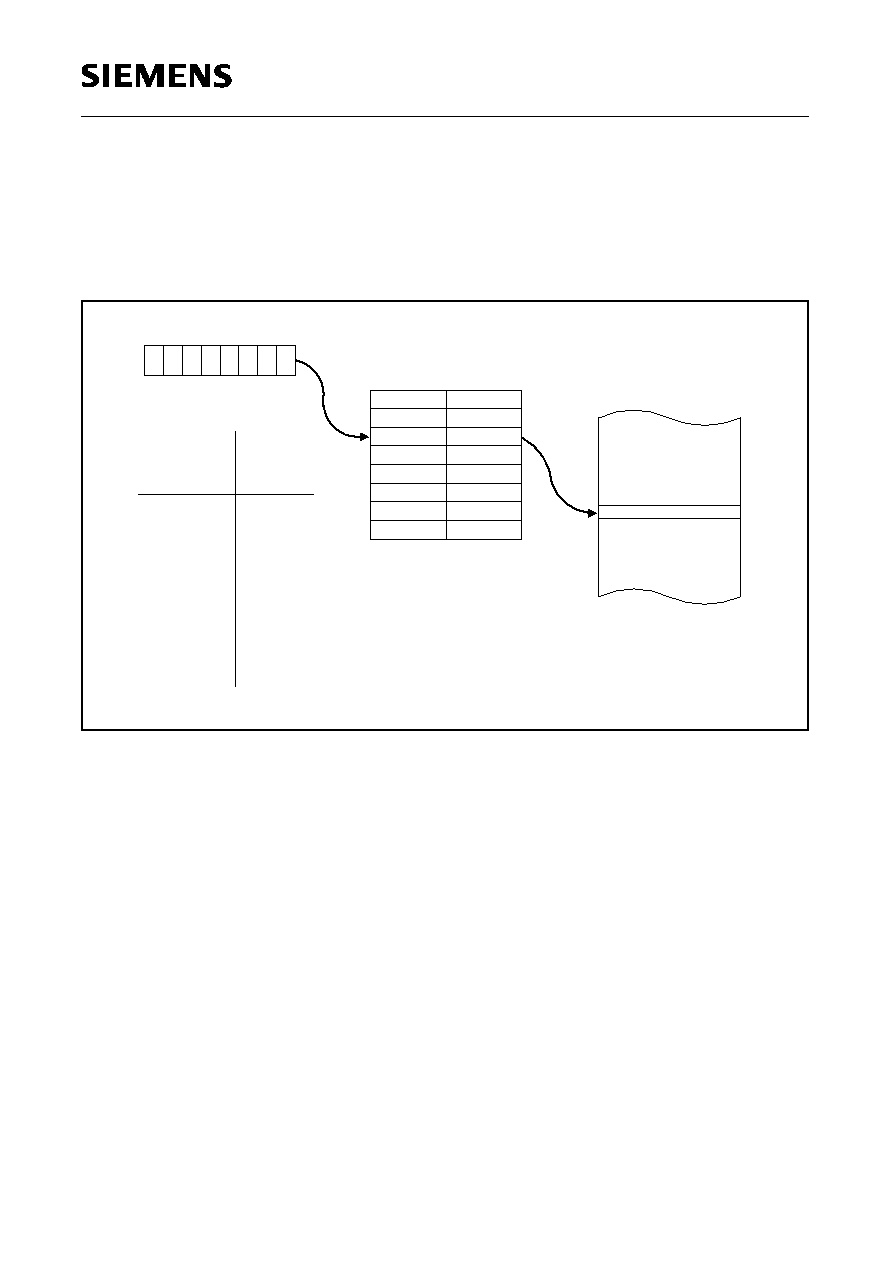
Figure 5 illustrates the memory address spaces of the C505 versions.
Figure 5
C505 Memory Map Memory Map
Ext.
Int.
(EA = 1)
Ext.
Data
Memory
Int. CAN
Contr.
(256 Byte)
(EA = 0)
Ext.
FFFF
H
8000
H
3FFF /
H
0000
H
Data
Memory
Ext.
F700
H
F6FF
H
0000
H
00
H
H
7F
Regs.
Function
Special
RAM
Internal
RAM
Internal
H
80
H
FF
Addr.
Indirect
Addr.
Direct
Alternatively
"Code Space"
"Data Space"
"Internal Data Space"
MCB03632
XRAM
Internal
FFFF
H
80
H
FF
H
See table below
for detailed
Data Memory
partitioning
H
4000 /
7FFF
H
Device
CAN Area
C505
C505C
C505A
C505CA
F700 F7FF
H
H
Unused Area
F800 FEFF
H
H
F700 FEFF
H
H
FF00 FFFF
XRAM Area
H
H
"Data Space" F700 to FFFF :
H
H
F700 F7FF
H
H
F800 FBFF
F700 FBFF
H
H
H
H
FF00 FFFF
H
H
FC00 FFFF
H
H
FC00 FFFF
H
H
Unused
Area

Semiconductor Group
16
1997-12-01
C505 / C505C
C505A / C505CA
Reset and System Clock
The reset input is an active high input at pin RESET. Since the reset is synchronized internally, the
RESET pin must be held high for at least two machine cycles (12 oscillator periods) while the
oscillator is running. A pulldown resistor is internally connected to
V
SS
to allow a power-up reset with
an external capacitor only. An automatic reset can be obtained when
V
CC
is applied by connecting
the RESET pin to
V
CC
via a capacitor. Figure 6 shows the possible reset circuitries.
Figure 6
Reset Circuitries
+
+
C505
RESET
c)
&
MCS03633
V
CC
CC
V
RESET
RESET
CC
V
C505C
C505CA
C505A
C505
C505CA
C505C
C505A
a)
C505A
C505C
C505CA
b)
C505

Semiconductor Group
17
1997-12-01
C505 / C505C
C505A / C505CA
Figure 7 shows the recommended oscillator circuits for crystal and external clock operation.
Figure 7
Recommended Oscillator Circuitries
MCS03634
C
2 - 20 MHz
XTAL2
XTAL1
C = 20 pF 10 pF for crystal operation
C
CC
External
Signal
Clock
V
N.C.
XTAL1
XTAL2
C505
C505C
C505A
C505CA
C505C
C505A
C505CA
C505
Semiconductor Group
18
1997-12-01
C505 / C505C
C505A / C505CA
Multiple Datapointers
As a functional enhancement to the standard 8051 architecture, the C505 contains eight 16-bit
datapointers instead of only one datapointer. The instruction set uses just one of these datapointers
at a time. The selection of the actual datapointer is done in the special function regsiter DPSEL.
Figure 8 illustrates the datapointer addressing mechanism.
Figure 8
External Data Memory Addressing using Multiple Datapointers
DPH(83 )
DPL(82 )
DPTR0
DPTR7
.0
.1
.2
-
-
-
-
-
DPSEL(92 )
DPSEL
Selected
Data-
pointer
.2
.1
.0
DPTR 0
0
0
0
0
0
1
DPTR 1
0
1
0
DPTR 2
0
1
1
DPTR 3
1
0
0
DPTR 4
1
0
1
DPTR 5
1
1
0
DPTR 6
1
1
1
DPTR 7
MCD00779
External Data Memory
H
H
H
Semiconductor Group
19
1997-12-01
C505 / C505C
C505A / C505CA
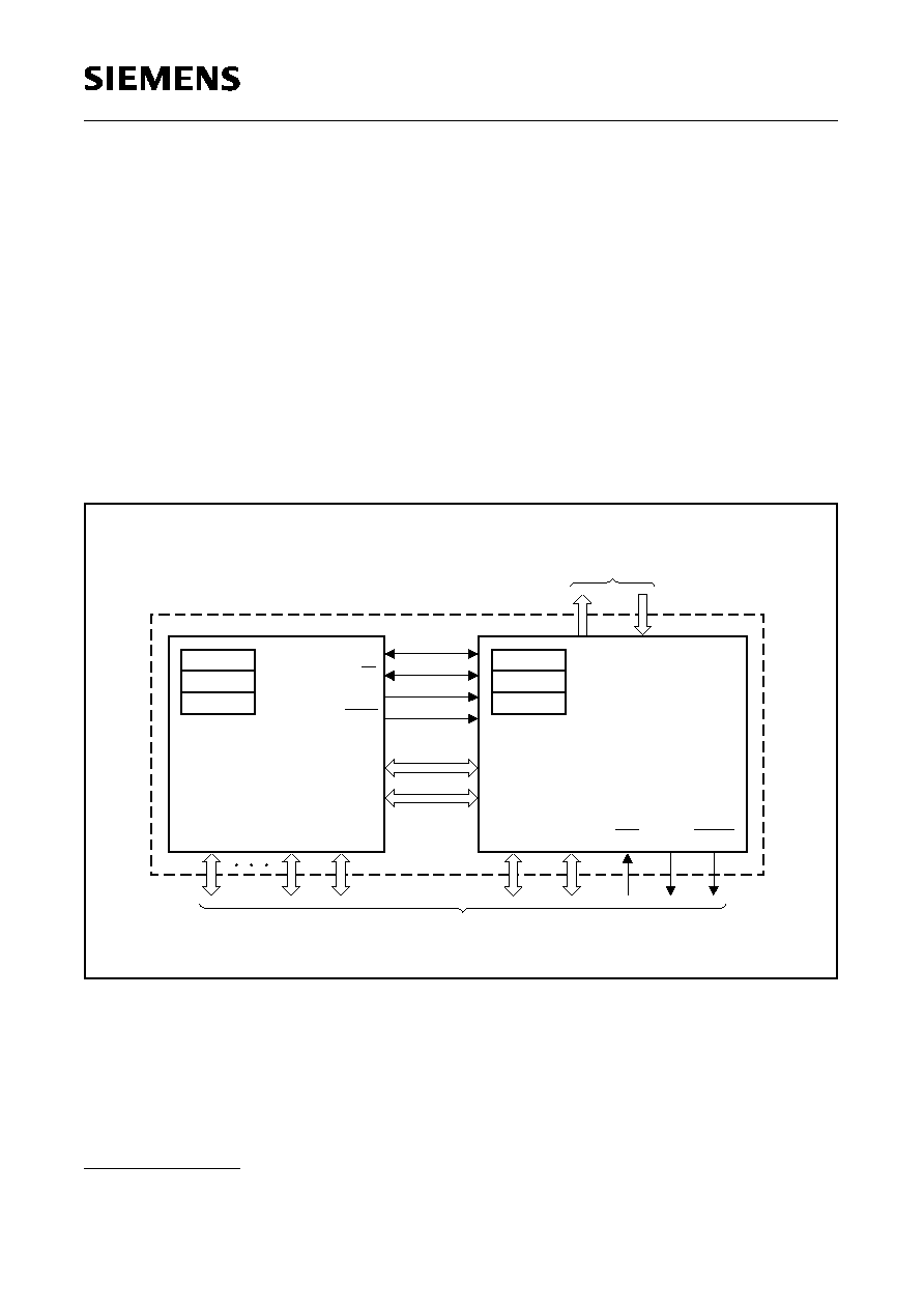
Enhanced Hooks Emulation Concept
The Enhanced Hooks Emulation Concept of the C500 microcontroller family is a new, innovative
way to control the execution of C500 MCUs and to gain extensive information on the internal
operation of the controllers. Emulation of on-chip ROM based programs is possible, too.
Each production chip has built-in logic for the supprt of the Enhanced Hooks Emulation Concept.
Therefore, no costly bond-out chips are necessary for emulation. This also ensure that emulation
and production chips are identical.
The Enhanced Hooks Technology
TM
1)
, which requires embedded logic in the C500 allows the C500
together with an EH-IC to function similar to a bond-out chip. This simplifies the design and reduces
costs of an ICE-system. ICE-systems using an EH-IC and a compatible C500 are able to emulate
all operating modes of the different versions of the C500 microcontrollers. This includes emulation
of ROM, ROM with code rollover and ROMless modes of operation. It is also able to operate in
single step mode and to read the SFRs after a break.
Figure 9
Basic C500 MCU Enhanced Hooks Concept Configuration
Port 0, port 2 and some of the control lines of the C500 based MCU are used by Enhanced Hooks
Emulation Concept to control the operation of the device during emulation and to transfer
informations about the program execution and data transfer between the external emulation
hardware (ICE-system) and the C500 MCU.
1)
"Enhanced Hooks Technology" is a trademark and patent of Metalink Corporation licensed to Siemens.
MCS02647
SYSCON
PCON
TCON
RESET
EA
PSEN
ALE
Port 0
Port 2
I/O Ports
Optional
Port 3
Port 1
C500
MCU
Interface Circuit
Enhanced Hooks
RPort 0
RPort 2
RTCON
RPCON
RSYSCON
TEA
TALE TPSEN
EH-IC
Target System Interface
ICE-System Interface
to Emulation Hardware
Semiconductor Group
20
1997-12-01
C505 / C505C
C505A / C505CA
Special Function Registers
The registers, except the program counter and the four general purpose register banks, reside in
the special function register area. The special function register area consists of two portions : the
standard special function register area and the mapped special function register area. Five special
function register of the C505 (PCON1,P1ANA, VR0, VR1, VR2) are located in the mapped special
function register area. For accessing the mapped special function register area, bit RMAP in special
function register SYSCON must be set. All other special function registers are located in the
standard special function register area which is accessed when RMAP is cleared ("0").
The registers and data locations of the CAN controller (CAN-SFRs) are located in the external data
memory area at addresses F700H to F7FFH..
Special Function Register SYSCON (Address B1H)
Reset Value : XX100X01B
(C505CA only) Reset Value : XX100001B
As long as bit RMAP is set, mapped special function register area can be accessed. This bit is not
cleared by hardware automatically. Thus, when non-mapped/mapped registers are to be accessed,
the bit RMAP must be cleared/set respectively by software.
All SFRs with addresses where address bits 0-2 are 0 (e.g. 80H, 88H, 90H, 98H, ..., F8H, FFH) are
bitaddressable.
The 52 special function registers (SFRs) in the standard and mapped SFR area include pointers
and registers that provide an interface between the CPU and the other on-chip peripherals. The
SFRs of the C505 are listed in table 4 and table 5. In table 4 they are organized in groups which
refer to the functional blocks of the C505. The CAN-SFRs (applicable for the C505C and C505CA
only) are also included in table 4. Table 5 illustrates the contents of the SFRs in numeric order of
their addresses. Table 6 list the CAN-SFRs in numeric order of their addresses. .
Bit
Function
RMAP
Special function register map bit
RMAP = 0 : The access to the non-mapped (standard) special function
register area is enabled.
RMAP = 1 : The access to the mapped special function register area is
enabled.
7
6
5
4
3
2
1
0
EALE
RMAP CMOD
B1H
SYSCON
Bit No.
MSB
LSB
CSWO XMAP1
≠
≠
XMAP0
The functions of the shaded bits are not described here.
1)
1) This bit is only available in the C505CA.

Semiconductor Group
21
1997-12-01
C505 / C505C
C505A / C505CA
Table 4
Special Function Registers - Functional Blocks
Block
Symbol
Name
Address
Contents after
Reset
CPU
ACC
B
DPH
DPL
DPSEL
PSW
SP
SYSCON
2)
VR0
4)
VR1
4)
VR2
4)
Accumulator
B-Register
Data Pointer, High Byte
Data Pointer, Low Byte
Data Pointer Select Register
Program Status Word Register
Stack Pointer
System Control Register
Version Register 0
Version Register 1
Version Register 2
E0H
1)
F0H
1)
83H
82H
92H
D0H
1)
81H
B1H
FCH
FDH
FDH
FEH
00H
00H
00H
00H
XXXXX000B
3)
00H
07H
XX100X01B
3) 6)
XX100001B
3) 7)
C5H
05H
6)
85H
7)
5)
A/D-
Converter
ADCON0
2)
ADCON1
ADDAT
ADST
ADDATH
ADDATL
P1ANA
2) 4)
A/D Converter Control Register 0
A/D Converter Control Register 1
A/D Converter Data Reg. (C505/C505C)
A/D Converter Start Reg. (C505/C505C)
A/D Converter High Byte Data Register
(C505A/C505CA)
A/D Converter Low Byte Data Register
(C505A/C505CA)
Port 1 Analog Input Selection Register
D8H
1)
DCH
D9H
DAH
D9H
DAH
90H
1)
00X00000B
3)
01XXX000B
3)
00H
XXH
3)
00H
00XXXXXXB
3)
FFH
Interrupt
System
IEN0
2)
IEN1
2)
IP0
2)
IP1
TCON
2)
T2CON
2)
SCON
2)
IRCON
Interrupt Enable Register 0
Interrupt Enable Register 1
Interrupt Priority Register 0
Interrupt Priority Register 1
Timer Control Register
Timer 2 Control Register
Serial Channel Control Register
Interrupt Request Control Register
A8H
1)
B8H
1)
A9H
B9H
88H
1)
C8H
1)
98H
1)
C0H
1)
00H
00H
00H
XX000000B
3)
00H
00X00000B
00H
00H
XRAM
XPAGE
SYSCON
2)
Page Address Register for Extended on-chip
XRAM and CAN Controller
System Control Register
91H
B1H
00H
XX100X01B
3) 6)
XX100001B
3) 7)
1)
Bit-addressable special function registers
2)
This special function register is listed repeatedly since some bits of it also belong to other functional blocks.
3)
"X" means that the value is undefined and the location is reserved
4)
This SFR is a mapped SFR. For accessing this SFR, bit RMAP in SFR SYSCON must be set.
5)
The content of this SFR varies with the actual step of the C505 (eg. 01
H
for the first step)
6)
C505 / C505A only
7)
C505C / C505CA only

Semiconductor Group
22
1997-12-01
C505 / C505C
C505A / C505CA
Ports
P0
P1
P1ANA
2) 4)
P2
P3
P4
Port 0
Port 1
Port 1 Analog Input Selection Register
Port 2
Port 3
Port 4
80H
1)
90H
1)
90H
1)
A0H
1)
B0H
1)
E8H
1)
FFH
FFH
FFH
FFH
FFH
XXXXXX11B
Serial
Channel
ADCON0
2)
PCON
2)
SBUF
SCON
SRELL
SRELH
A/D Converter Control Register 0
Power Control Register
Serial Channel Buffer Register
Serial Channel Control Register
Serial Channel Reload Register, low byte
Serial Channel Reload Register, high byte
D8H
1)
87H
99H
98H
1)
AAH
BAH
00X00000B
3)
00H
XXH
3)
00H
D9H
XXXXXX11B
3)
Timer 0/
Timer 1
TCON
TH0
TH1
TL0
TL1
TMOD
Timer 0/1 Control Register
Timer 0, High Byte
Timer 1, High Byte
Timer 0, Low Byte
Timer 1, Low Byte
Timer Mode Register
88H
1)
8CH
8DH
8AH
8BH
89H
00H
00H
00H
00H
00H
00H
Compare/
Capture
Unit /
Timer 2
CCEN
CCH1
CCH2
CCH3
CCL1
CCL2
CCL3
CRCH
CRCL
TH2
TL2
T2CON
IEN0
2)
IEN1
2)
Comp./Capture Enable Reg.
Comp./Capture Reg. 1, High Byte
Comp./Capture Reg. 2, High Byte
Comp./Capture Reg. 3, High Byte
Comp./Capture Reg. 1, Low Byte
Comp./Capture Reg. 2, Low Byte
Comp./Capture Reg. 3, Low Byte
Reload Register High Byte
Reload Register Low Byte
Timer 2, High Byte
Timer 2, Low Byte
Timer 2 Control Register
Interrupt Enable Register 0
Interrupt Enable Register 1
C1H
C3H
C5H
C7H
C2H
C4H
C6H
CBH
CAH
CDH
CCH
C8H
1)
A8H
1)
B8H
1)
00H
3)
00H
00H
00H
00H
00H
00H
00H
00H
00H
00H
00X00000B
3)
00H
00H
Watchdog WDTREL
IEN0
2)
IEN1
2)
IP0
2)
Watchdog Timer Reload Register
Interrupt Enable Register 0
Interrupt Enable Register 1
Interrupt Priority Register 0
86H
A8H
1)
B8H
1)
A9H
00H
00H
00H
00H
Pow. Save
Modes
PCON
2)
PCON1
4)
Power Control Register
Power Control Register 1
87H
88H
1)
00H
0XX0XXXXB
3)
1)
Bit-addressable special function registers
2)
This special function register is listed repeatedly since some bits of it also belong to other functional blocks.
3)
"X" means that the value is undefined and the location is reserved
4)
SFR is located in the mapped SFR area. For accessing this SFR, bit RMAP in SFR SYSCON must be set.
Table 4
Special Function Registers - Functional Blocks (cont'd)
Block
Symbol
Name
Address
Contents after
Reset
Semiconductor Group
23
1997-12-01
C505 / C505C
C505A / C505CA
CAN
Controller
(C505C/
C505CA
only)
CR
SR
IR
BTR0
BTR1
GMS0
GMS1
UGML0
UGML1
LGML0
LGML1
UMLM0
UMLM1
LMLM0
LMLM1
MCR0
MCR1
UAR0
UAR1
LAR0
LAR1
MCFG
DB0n
DB1n
DB2n
DB3n
DB4n
DB5n
DB6n
DB7n
Control Register
Status Register
Interrupt Register
Bit Timing Register Low
Bit Timing Register High
Global Mask Short Register Low
Global Mask Short Register High
Upper Global Mask Long Register Low
Upper Global Mask Long Register High
Lower Global Mask Long Register Low
Lower Global Mask Long Register High
Upper Mask of Last Message Register Low
Upper Mask of Last Message Register High
Lower Mask of Last Message Register Low
Lower Mask of Last Message Register High
Message Object Registers :
Message Control Register Low
Message Control Register High
Upper Arbitration Register Low
Upper Arbitration Register High
Lower Arbitration Register Low
Lower Arbitration Register High
Message Configuration Register
Message Data Byte 0
Message Data Byte 1
Message Data Byte 2
Message Data Byte 3
Message Data Byte 4
Message Data Byte 5
Message Data Byte 6
Message Data Byte 7
F700H
F701H
F702H
F704H
F705H
F706H
F707H
F708H
F709H
F70AH
F70BH
F70CH
F70DH
F70EH
F70FH
F7n0H
5)
F7n1H
5)
F7n2H
5)
F7n3H
5)
F7n4H
5)
F7n5H
5)
F7n6H
5)
F7n7H
5)
F7n8H
5)
F7n9H
5)
F7nAH
5)
F7nBH
5)
F7nCH
5)
F7nDH
5)
F7nEH
5)
01H
XXH
3)
XXH
3)
UUH
3)
0UUUUUUU
B
3)
UUH
3)
UUU11111
B
3)
UUH
3)
UUH
3)
UUH
3)
UUUUU000
B
3)
UUH
3)
UUH
3)
UUH
3)
UUUUU000
B
3)
UUH
3)
UUH
3)
UUH
3)
UUH
3)
UUH
3)
UUUUU000
B
3)
UUUUUU00
B
3)
XXH
3)
XXH
3)
XXH
3)
XXH
3)
XXH
3)
XXH
3)
XXH
3)
XXH
3)
1) Bit-addressable special function registers
2) This special function register is listed repeatedly since some bits of it also belong to other functional blocks.
3) "X" means that the value is undefined and the location is reserved. "U" means that the value is unchanged
by a reset operation. "U" values are undefined (as "X") after a power-on reset operation
4) SFR is located in the mapped SFR area. For accessing this SFR, bit RMAP in SFR SYSCON must be set.
5) The notation "n" (n= 1 to F) in the message object address definition defines the number of the related
message object.
Table 4
Special Function Registers - Functional Blocks (cont'd)
Block
Symbol
Name
Address
Contents after
Reset
Semiconductor Group
24
1997-12-01
C505 / C505C
C505A / C505CA
Table 5
Contents of the SFRs, SFRs in numeric order of their addresses
Addr
Register Content
after
Reset
1)
Bit 7
Bit 6
Bit 5
Bit 4
Bit 3
Bit 2
Bit 1
Bit 0
80H
2)
P0
FFH
.7
.6
.5
.4
.3
.2
.1
.0
81H
SP
07H
.7
.6
.5
.4
.3
.2
.1
.0
82H
DPL
00H
.7
.6
.5
.4
.3
.2
.1
.0
83H
DPH
00H
.7
.6
.5
.4
.3
.2
.1
.0
86H
WDTREL 00H
WDT
PSEL
.6
.5
.4
.3
.2
.1
.0
87H
PCON
00H
SMOD PDS
IDLS
SD
GF1
GF0
PDE
IDLE
88H
2)
TCON
00H
TF1
TR1
TF0
TR0
IE1
IT1
IE0
IT0
88H
3)
PCON1
0XX0-
XXXXB
EWPD ≠
≠
WS
≠
≠
≠
≠
89H
TMOD
00H
GATE
C/T
M1
M0
GATE
C/T
M1
M0
8AH
TL0
00H
.7
.6
.5
.4
.3
.2
.1
.0
8BH
TL1
00H
.7
.6
.5
.4
.3
.2
.1
.0
8CH
TH0
00H
.7
.6
.5
.4
.3
.2
.1
.0
8DH
TH1
00H
.7
.6
.5
.4
.3
.2
.1
.0
90H
2)
P1
FFH
T2
CLK-
OUT
T2EX
.4
.3
INT5
INT4
.0
90H
3)
P1ANA
FFH
EAN7
EAN6
EAN5
EAN4
EAN3
EAN2
EAN1
EAN0
91H
XPAGE
00H
.7
.6
.5
.4
.3
.2
.1
.0
92H
DPSEL
XXXX-
X000B
≠
≠
≠
≠
≠
.2
.1
.0
98H
2)
SCON
00H
SM0
SM1
SM2
REN
TB8
RB8
TI
RI
99H
SBUF
XXH
.7
.6
.5
.4
.3
.2
.1
.0
A0H
2)
P2
FFH
.7
.6
.5
.4
.3
.2
.1
.0
A8H
2)
IEN0
00H
EA
WDT
ET2
ES
ET1
EX1
ET0
EX0
A9H
IP0
00H
OWDS WDTS
.5
.4
.3
.2
.1
.0
AAH
SRELL
D9H
.7
.6
.5
.4
.3
.2
.1
.0
1)
X means that the value is undefined and the location is reserved
2)
Bit-addressable special function registers
3)
SFR is located in the mapped SFR area. For accessing this SFR, bit RMAP in SFR SYSCON must be set.

Semiconductor Group
25
1997-12-01
C505 / C505C
C505A / C505CA
B0H
2)
P3
FFH
RD
WR
T1
T0
INT1
INT0
TxD
RxD
B1H
SYSCON
4)
XX10-
0X01B
≠
≠
EALE
RMAP
CMOD ≠
XMAP1 XMAP0
B1H
SYSCON
4)
XX10-
0001B
≠
≠
EALE
RMAP
CMOD CSWO XMAP1 XMAP0
B8H
2)
IEN1
3)
00H
EXEN2 SWDT
EX6
EX5
EX4
EX3
0
EADC
B8H
2)
IEN1
4)
00H
EXEN2 SWDT
EX6
EX5
EX4
EX3
ECAN
EADC
B9H
IP1
XX00-
0000B
≠
≠
.5
.4
.3
.2
.1
.0
BAH
SRELH
XXXX-
XX11B
≠
≠
≠
≠
≠
≠
.1
.0
C0H
2)
IRCON
00H
EXF2
TF2
IEX6
IEX5
IEX4
IEX3
SWI
IADC
C1H
CCEN
00H
COCA
H3
COCAL
3
COCA
H2
COCAL
2
COCA
H1
COCAL
1
COCA
H0
COCAL
0
C2H
CCL1
00H
.7
.6
.5
.4
.3
.2
.1
.0
C3H
CCH1
00H
.7
.6
.5
.4
.3
.2
.1
.0
C4H
CCL2
00H
.7
.6
.5
.4
.3
.2
.1
.0
C5H
CCH2
00H
.7
.6
.5
.4
.3
.2
.1
.0
C6H
CCL3
00H
.7
.6
.5
.4
.3
.2
.1
.0
C7H
CCH3
00H
.7
.6
.5
.4
.3
.2
.1
.0
C8H
2)
T2CON
00X0-
0000B
T2PS
I3FR
≠
T2R1
T2R0
T2CM
T2I1
T2I0
CAH
CRCL
00H
.7
.6
.5
.4
.3
.2
.1
.0
CBH
CRCH
00H
.7
.6
.5
.4
.3
.2
.1
.0
CCH
TL2
00H
.7
.6
.5
.4
.3
.2
.1
.0
CDH
TH2
00H
.7
.6
.5
.4
.3
.2
.1
.0
D0H
2)
PSW
00H
CY
AC
F0
RS1
RS0
OV
F1
P
D8H
2)
ADCON0 00X0-
0000B
BD
CLK
≠
BSY
ADM
MX2
MX1
MX0
D9H ADDAT
3)
00H
.7
.6
.5
.4
.3
.2
.1
.0
1)
X means that the value is undefined and the location is reserved
2)
Bit-addressable special function registers
3)
C505 / C505A only
4)
C505C / C505CA only
Table 5
Contents of the SFRs, SFRs in numeric order of their addresses (cont'd)
Addr
Register Content
after
Reset
1)
Bit 7
Bit 6
Bit 5
Bit 4
Bit 3
Bit 2
Bit 1
Bit 0

Semiconductor Group
26
1997-12-01
C505 / C505C
C505A / C505CA
D9H
ADDATH
7)
00H
.9
.8
.7
.6
.5
.4
.3
.2
DAH
ADST
6)
XXXX-
XXXXB
≠
≠
≠
≠
≠
≠
≠
≠
DAH
ADDATL
7)
00XX-
XXXXB
.1
.0
≠
≠
≠
≠
≠
≠
DCH
ADCON1 01XX-
X000B
ADCL1 ADCL0 ≠
≠
≠
MX2
MX1
MX0
E0H
2)
ACC
00H
.7
.6
.5
.4
.3
.2
.1
.0
E8H
2)
P4
XXXX-
XX11B
≠
≠
≠
≠
≠
≠
RXDC
TXDC
F0H
2)
B
00H
.7
.6
.5
.4
.3
.2
.1
.0
FCH
3)4)
VR0
C5H
1
1
0
0
0
1
þ
1
FDH
3)4)
VR1
05H
0
0
0
0
0
1
0
1
FEH
3)4)
VR2
01H
5) 6)
11H
5) 7)
.7
.6
.5
.4
.3
.2
.1
.0
1)
X means that the value is undefined and the location is reserved
2)
Bit-addressable special function registers
3)
SFR is located in the mapped SFR area. For accessing this SFR, bit RMAP in SFR SYSCON must be set.
4)
These are read-only registers
5)
The content of this SFR varies with the actual of the step C505 (eg. 01
H
or 11
H
for the first step)
6)
C505 / C505C only
7)
C505A / C505CA only
Table 5
Contents of the SFRs, SFRs in numeric order of their addresses (cont'd)
Addr
Register Content
after
Reset
1)
Bit 7
Bit 6
Bit 5
Bit 4
Bit 3
Bit 2
Bit 1
Bit 0
Semiconductor Group
27
1997-12-01
C505 / C505C
C505A / C505CA
Table 6
Contents of the CAN Registers in numeric order of their addresses
(C505C/C505CA only)
Addr.
n=1-FH
1)
Register Content
after
Reset
2)
Bit 7
Bit 6
Bit 5
Bit 4
Bit 3
Bit 2
Bit 1
Bit 0
F700H CR
01H
TEST
CCE
0
0
EIE
SIE
IE
INIT
F701H SR
XXH
BOFF
EWRN ≠
RXOK TXOK
LEC2
LEC1
LEC0
F702H IR
XXH
INTID
F704H BTR0
UUH
SJW
BRP
F705H BTR1
0UUU.
UUUUB
0
TSEG2
TSEG1
F706H GMS0
UUH
ID28-21
F707H GMS1
UUU1.
1111B
ID20-18
1
1
1
1
1
F708H UGML0
UUH
ID28-21
F709H UGML1
UUH
ID20-13
F70AH LGML0
UUH
ID12-5
F70BH LGML1
UUUU.
U000B
ID4-0
0
0
0
F70CH UMLM0
UUH
ID28-21
F70DH UMLM1
UUH
ID20-18
ID17-13
F70EH LMLM0
UUH
ID12-5
F70FH LMLM1
UUUU.
U000B
ID4-0
0
0
0
F7n0H MCR0
UUH
MSGVAL
TXIE
RXIE
INTPND
F7n1H MCR1
UUH
RMTPND
TXRQ
MSGLST
CPUUPD
NEWDAT
F7n2H UAR0
UUH
ID28-21
F7n3H UAR1
UUH
ID20-18
ID17-13
F7n4H LAR0
UUH
ID12-5
F7n5H LAR1
UUUU.
U000B
ID4-0
0
0
0
F7n6H MCFG
UUUU.
UU00B
DLC
DIR
XTD
0
0
1)
The notation "n" (n= 1 to F) in the address definition defines the number of the related message object.
2)
"X" means that the value is undefined and the location is reserved. "U" means that the value is unchanged
by a reset operation. "U" values are undefined (as "X") after a power-on reset operation
Semiconductor Group
28
1997-12-01
C505 / C505C
C505A / C505CA
F7n7H DB0n
XXH
.7
.6
.5
.4
.3
.2
.1
.0
F7n8H DB1n
XXH
.7
.6
.5
.4
.3
.2
.1
.0
F7n9H DB2n
XXH
.7
.6
.5
.4
.3
.2
.1
.0
F7nAH DB3n
XXH
.7
.6
.5
.4
.3
.2
.1
.0
F7nBH DB4n
XXH
.7
.6
.5
.4
.3
.2
.1
.0
F7nCH DB5n
XXH
.7
.6
.5
.4
.3
.2
.1
.0
F7nDH DB6n
XXH
.7
.6
.5
.4
.3
.2
.1
.0
F7nEH DB7n
XXH
.7
.6
.5
.4
.3
.2
.1
.0
1)
The notation "n" (n= 1 to F) in the address definition defines the number of the related message object.
2)
"X" means that the value is undefined and the location is reserved. "U" means that the value is unchanged
by a reset operation. "U" values are undefined (as "X" after a power-on reset operation
Table 6
Contents of the CAN Registers in numeric order of their addresses (cont'd)
(C505C/C505CA only)
Addr.
n=1-FH
1)
Register Content
after
Reset
2)
Bit 7
Bit 6
Bit 5
Bit 4
Bit 3
Bit 2
Bit 1
Bit 0

Semiconductor Group
29
1997-12-01
C505 / C505C
C505A / C505CA
I/O Ports
The C505 has four 8-bit I/O ports and one 2-bit I/O port. Port 0 is an open-drain bidirectional I/O
port, while ports 1 to 4 are quasi-bidirectional I/O ports with internal pullup resistors. That means,
when configured as inputs, ports 1 to 4 will be pulled high and will source current when externally
pulled low. Port 0 will float when configured as input.
The output drivers of port 0 and 2 and the input buffers of port 0 are also used for accessing external
memory. In this application, port 0 outputs the low byte of the external memory address, time
multiplexed with the byte being written or read. Port 2 outputs the high byte of the external memory
address when the address is 16 bits wide. Otherwise, the port 2 pins continue emitting the P2 SFR
contents. In this function, port 0 is not an open-drain port, but uses a strong internal pullup FET.
Port 4 is 2-bit I/O port with CAN controller specific alternate functions. The eight analog input lines
are realized as mixed digital/analog inputs. The 8 analog inputs, AN0-AN7, are located at the port 1
pins P1.0 to P1.7. After reset, all analog inputs are disabled and the related pins of port 1 are
configured as digital inputs. The analog function of a specific port 1 pin is enabled by bits in the SFR
P1ANA. Writing a 0 to a bit position of P1ANA assigns the corresponding pin to operate as analog
input.
Note: P1ANA is a mapped SFR and can be only accessed if bit RMAP in SFR SYSCON is set.

Semiconductor Group
30
1997-12-01
C505 / C505C
C505A / C505CA
Timer / Counter 0 and 1
Timer/Counter 0 and 1 can be used in four operating modes as listed in table 7 :
In the "timer" function (C/T = `0') the register is incremented every machine cycle. Therefore the
count rate is
f
OSC
/6.
In the "counter" function the register is incremented in response to a 1-to-0 transition at its
corresponding external input pin (P3.4/T0, P3.5/T1). Since it takes two machine cycles to detect a
falling edge the max. count rate is
f
OSC
/12. External inputs INT0 and INT1 (P3.2, P3.3) can be
programmed to function as a gate to facilitate pulse width measurements. Figure 10 illustrates the
input clock logic.
Figure 10
Timer/Counter 0 and 1 Input Clock Logic
Table 7
Timer/Counter 0 and 1 Operating Modes
Mode
Description
TMOD
Input Clock
M1
M0
internal
external (max)
0
8-bit timer/counter with a
divide-by-32 prescaler
0
0
f
OSC
/6x32
f
OSC
/12x32
1
16-bit timer/counter
1
1
f
OSC
/6
f
OSC
/12
2
8-bit timer/counter with
8-bit autoreload
1
0
3
Timer/counter 0 used as one
8-bit timer/counter and one
8-bit timer
Timer 1 stops
1
1
MCS03117
1
&
OSC
C/T = 0
C/T = 1
Control
=1
6
TR1
P3.5/T1
(TMOD)
P3.2/INT0
f
Timer 0/1
Input Clock
OSC
/6
P3.4/T0
TR0
Gate
P3.3/INT1
˜
_
<

Semiconductor Group
31
1997-12-01
C505 / C505C
C505A / C505CA
Timer/Counter 2 with Compare/Capture/Reload
The timer 2 of the C505 provides additional compare/capture/reload features. which allow the
selection of the following operating modes:
≠ Compare
: up to 4 PWM signals with 16-bit/300 ns resolution (@ 20 MHz clock)
≠ Capture
: up to 4 high speed capture inputs with 300 ns resolution
≠ Reload
: modulation of timer 2 cycle time
The block diagram in figure 11 shows the general configuration of timer 2 with the additional
compare/capture/reload registers. The I/O pins which can used for timer 2 control are located as
multifunctional port functions at port 1.
Figure 11
Timer 2 Block Diagram
MCB02730
Comparator
CCL3/CCH3
Capture
Input/
Output
Control
P1.0/
INT3/
CC0
CC1
INT4/
P1.1/
CC2
INT5/
P1.2/
CC3
INT6/
P1.2/
CCL2/CCH2
Comparator
CCL1/CCH1
Comparator
CRCL/CRCH
Comparator
Bit
16
16 Bit
16 Bit
16 Bit
OSC
˜6
˜12
f
OSC
T2PS
Sync.
P1.7/
T2
T2EX
P1.5/
Sync.
&
T2I1
T2I0
Timer 2
TH2
TL2
TF2
Reload
EXEN2
Reload
1
EXF2
Interrupt
Request
Compare
_
<

Semiconductor Group
32
1997-12-01
C505 / C505C
C505A / C505CA
Timer 2 Operating Modes
The timer 2, which is a 16-bit-wide register, can operate as timer, event counter, or gated timer. A
roll-over of the count value in TL2/TH2 from all 1's to all 0's sets the timer overflow flag TF2 in SFR
IRCON, which can generate an interrupt. The bits in register T2CON are used to control the timer 2
operation.
Timer Mode : In timer function, the count rate is derived from the oscillator frequency. A prescaler
offers the possibility of selecting a count rate of 1/6 or 1/12 of the oscillator frequency.
Gated Timer Mode : In gated timer function, the external input pin T2 (P1.7) functions as a gate to
the input of timer 2. lf T2 is high, the internal clock input is gated to the timer. T2 = 0 stops the
counting procedure. This facilitates pulse width measurements. The external gate signal is sampled
once every machine cycle.
Event Counter Mode : In the event counter function. the timer 2 is incremented in response to a 1-
to-0 transition at its corresponding external input pin T2 (P1.7). In this function, the external input is
sampled every machine cycle. Since it takes two machine cycles (12 oscillator periods) to recognize
a 1-to-0 transition, the maximum count rate is 1/6 of the oscillator frequency. There are no
restrictions on the duty cycle of the external input signal, but to ensure that a given level is sampled
at least once before it changes, it must be held for at least one full machine cycle.
Reload of Timer 2 : Two reload modes are selectable:
In mode 0, when timer 2 rolls over from all 1's to all 0's, it not only sets TF2 but also causes the timer
2 registers to be loaded with the 16-bit value in the CRC register, which is preset by software.
In mode 1, a 16-bit reload from the CRC register is caused by a negative transition at the correspon-
ding input pin P1.5/T2EX. This transition will also set flag EXF2 if bit EXEN2 in SFR IEN1 has been
set.
Semiconductor Group
33
1997-12-01
C505 / C505C
C505A / C505CA
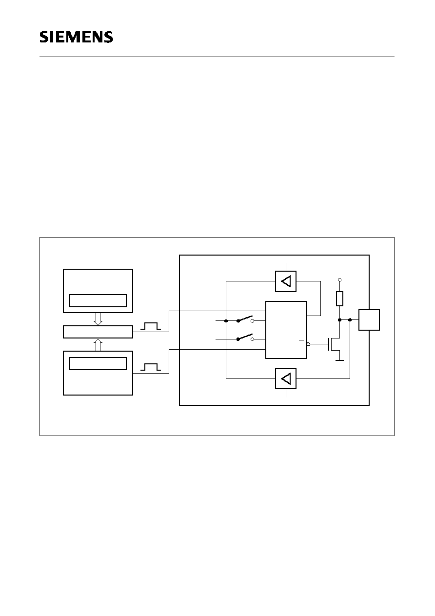
Timer 2 Compare Modes
The compare function of a timer/register combination operates as follows : the 16-bit value stored
in a compare or compare/capture register is compared with the contents of the timer register; if the
count value in the timer register matches the stored value, an appropriate output signal is generated
at a corresponding port pin and an interrupt can be generated.
Compare Mode 0
In compare mode 0, upon matching the timer and compare register contents, the output signal
changes from low to high. lt goes back to a low level on timer overflow. As long as compare mode 0
is enabled, the appropriate output pin is controlled by the timer circuit only and writing to the port
will have no effect. Figure 12 shows a functional diagram of a port circuit when used in compare
mode 0. The port latch is directly controlled by the timer overflow and compare match signals. The
input line from the internal bus and the write-to-latch line of the port latch are disconnected when
compare mode 0 is enabled.
Figure 12
Port Latch in Compare Mode 0
MCS02661
Latch
Port
Q
Q
CLK
D
Port
Pin
Read Pin
CC
V
Read Latch
Port Circuit
Internal
Bus
Latch
Write to
Compare Reg.
Compare Register
Circuit
Comparator
Timer Register
Timer Circuit
Compare
Match
S
R
Overflow
Timer
16 Bit
Bit
16

Semiconductor Group
34
1997-12-01
C505 / C505C
C505A / C505CA
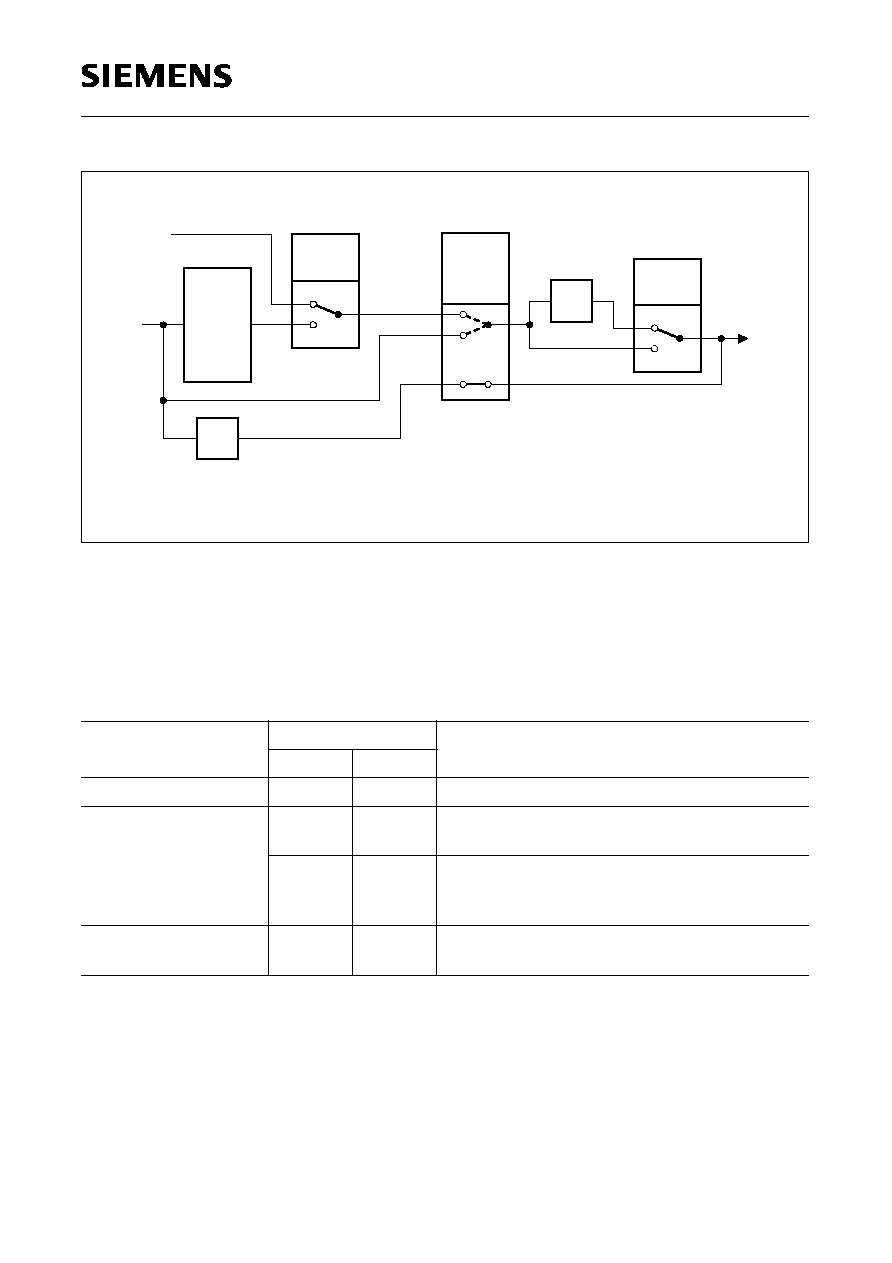
Compare Mode 1
If compare mode 1 is enabled and the software writes to the appropriate output latch at the port, the
new value will not appear at the output pin until the next compare match occurs. Thus, it can be
choosen whether the output signal has to make a new transition (1-to-0 or 0-to-1, depending on the
actual pin-level) or should keep its old value at the time when the timer value matches the stored
compare value.
In compare mode 1 (see figure 13) the port circuit consists of two separate latches. One latch
(which acts as a "shadow latch") can be written under software control, but its value will only be
transferred to the port latch (and thus to the port pin) when a compare match occurs.
Figure 13
Compare Function in Compare Mode 1
Timer 2 Capture Modes
Each of the compare/capture registers CC1 to CC3 and the CRC register can be used to latch the
current 16-bit value of the timer 2 registers TL2 and TH2. Two different modes are provided for this
function.
In mode 0, the external event causing a capture is :
≠ for CC registers 1 to 3: a positive transition at pins CC1 to CC3 of port 1
≠ for the CRC register:
a positive or negative transition at the corresponding pin, depending
on the status of the bit I3FR in SFR T2CON.
In mode 1 a capture occurs in response to a write instruction to the low order byte of a capture
register. The write-to-register signal (e.g. write-to-CRCL) is used to initiate a capture. The timer 2
contents will be latched into the appropriate capture register in the cycle following the write
instruction. In this mode no interrupt request will be generated.
MCS02662
Latch
Port
Q
Q
CLK
D
Read Pin
CC
V
D
CLK
Q
Shadow
Latch
Read Latch
Port Circuit
Internal
Bus
Latch
Write to
Compare Reg.
Compare Register
Circuit
Comparator
Timer Register
Timer Circuit
Compare
Match
Pin
Port
16 Bit
16 Bit
Semiconductor Group
35
1997-12-01
C505 / C505C
C505A / C505CA
Serial Interface (USART)
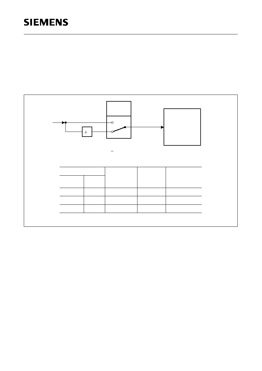
The serial port is full duplex and can operate in four modes (one synchronous mode, three
asynchronous modes) as illustrated in table 8.
For clarification some terms regarding the difference between "baud rate clock" and "baud rate"
should be mentioned. In the asynchronous modes the serial interfaces require a clock rate which is
16 times the baud rate for internal synchronization. Therefore, the baud rate generators/timers have
to provide a "baud rate clock" (output signal in figure 14 to the serial interface which - there divided
by 16 - results in the actual "baud rate". Further, the abbrevation f
OSC
refers to the oscillator
frequency (crystal or external clock operation).
The variable baud rates for modes 1 and 3 of the serial interface can be derived either from timer 1
or from a decdicated baud rate generator (see figure 14).
Table 8
USART Operating Modes
Mode
SCON
Description
SM0
SM1
0
0
0
Shift register mode, fixed baud rate
Serial data enters and exits through R
◊
D; T
◊
D outputs the shift
clock; 8-bit are transmitted/received (LSB first)
1
0
1
8-bit UART, variable baud rate
10 bits are transmitted (through T
◊
D) or received (at R
◊
D)
2
1
0
9-bit UART, fixed baud rate
11 bits are transmitted (through T
◊
D) or received (at R
◊
D)
3
1
1
9-bit UART, variable baud rate
Like mode 2
Semiconductor Group
36
1997-12-01
C505 / C505C
C505A / C505CA
Figure 14
Block Diagram of Baud Rate Generation for the Serial Interface
Table 9 below lists the values/formulas for the baud rate calculation of the serial interface with its
dependencies of the control bits BD and SMOD.
Table 9
Serial Interface - Baud Rate Dependencies
Serial Interface
Operating Modes
Active Control Bits Baud Rate Calculation
BD
SMOD
Mode 0 (Shift Register)
≠
≠
f
OSC
/ 6
Mode 1 (8-bit UART)
Mode 3 (9-bit UART)
0
X
Controlled by timer 1 overflow :
(2
SMOD
◊
timer 1 overflow rate) / 32
1
X
Controlled by baud rate generator
(2
SMOD
◊
f
OSC
) /
(32
◊
baud rate generator overflow rate)
Mode 2 (9-bit UART)
≠
0
1
f
OSC
/ 32
f
OSC
/ 16
MCS02733
Rate
f
OSC
(SMOD)
Baud
Clock
PCON.7
2
(SM0/
SM1)
SCON.7
SCON.6
Only one mode
can be selected
ADCON0.7
(BD)
0
1
0
1
Baud
Rate
Generator
(SRELH
SRELL)
Timer 1
Mode 2
Mode 0
Note: The switch configuration shows the reset state.
Mode 3
Mode 1
Overflow
6
˜
˜
Semiconductor Group
37
1997-12-01
C505 / C505C
C505A / C505CA
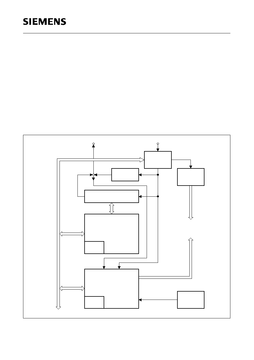
CAN Controller (C505C and C505CA only)
The on-chip CAN controller, compliant to version 2.0B, is the functional heart which provides all
resources that are required to run the standard CAN protocol (11-bit identifiers) as well as the
extended CAN protocol (29-bit identifiers). It provides a sophisticated object layer to relieve the
CPU of as much overhead as possible when controlling many different message objects (up to 15).
This includes bus arbitration, resending of garbled messages, error handling, interrupt generation,
etc. In order to implement the physical layer, external components have to be connected to the
C505.
The internal bus interface connects the on-chip CAN controller to the internal bus of the
microcontroller. The registers and data locations of the CAN interface are mapped to a specific
256 byte wide address range of the external data memory area (F700H to F7FFH) and can be
accessed using MOVX instructions. Figure 15 shows a block diagram of the on-chip CAN
controller.
Figure 15
CAN Controller Block Diagram
MCB02736
Bit
Timing
Logic
Timing
Generator
BTL-Configuration
CRC
Gen./Check
TX/RX Shift Register
TXDC
RXDC
Intelligent
Interrupt
Register
Memory
Processor
Register
Status
Stream
Bit
Error
Logic
Management
Messages
Handlers
Control
Status +
to internal Bus
Clocks
Control
Messages
(to all)

Semiconductor Group
38
1997-12-01
C505 / C505C
C505A / C505CA
The TX/RX Shift Register holds the destuffed bit stream from the bus line to allow the parallel
access to the whole data or remote frame for the acceptance match test and the parallel transfer of
the frame to and from the Intelligent Memory.
The Bit Stream Processor (BSP) is a sequencer controlling the sequential data stream between
the TX/RX Shift Register, the CRC Register, and the bus line. The BSP also controls the EML and
the parallel data stream between the TX/RX Shift Register and the Intelligent Memory such that the
processes of reception, arbitration, transmission, and error signalling are performed according to
the CAN protocol. Note that the automatic retransmission of messages which have been corrupted
by noise or other external error conditions on the bus line is handled by the BSP.
The Cyclic Redundancy Check Register (CRC) generates the Cyclic Redundancy Check code to
be transmitted after the data bytes and checks the CRC code of incoming messages. This is done
by dividing the data stream by the code generator polynomial.
The Error Management Logic (EML) is responsible for the fault confinement of the CAN device. Its
counters, the Receive Error Counter and the Transmit Error Counter, are incremented and
decremented by commands from the Bit Stream Processor. According to the values of the error
counters, the CAN controller is set into the states error
active
, error
passive
and busoff.
The Bit Timing Logic (BTL) monitors the busline input RXDC and handles the busline related bit
timing according to the CAN protocol. The BTL synchronizes on a
recessive
to
dominant
busline
transition at
Start of Frame
(hard synchronization) and on any further
recessive
to
dominant
busline
transition, if the CAN controller itself does not transmit a
dominant
bit (resynchronization). The BTL
also provides programmable time segments to compensate for the propagation delay time and for
phase shifts and to define the position of the Sample Point in the bit time. The programming of the
BTL depends on the baudrate and on external physical delay times.
The Intelligent Memory (CAM/RAM array) provides storage for up to 15 message objects of
maximum 8 data bytes length. Each of these objects has a unique identifier and its own set of
control and status bits. After the initial configuration, the Intelligent Memory can handle the
reception and transmission of data without further microcontroller actions.
Semiconductor Group
39
1997-12-01
C505 / C505C
C505A / C505CA
CAN Controller Software Initialization
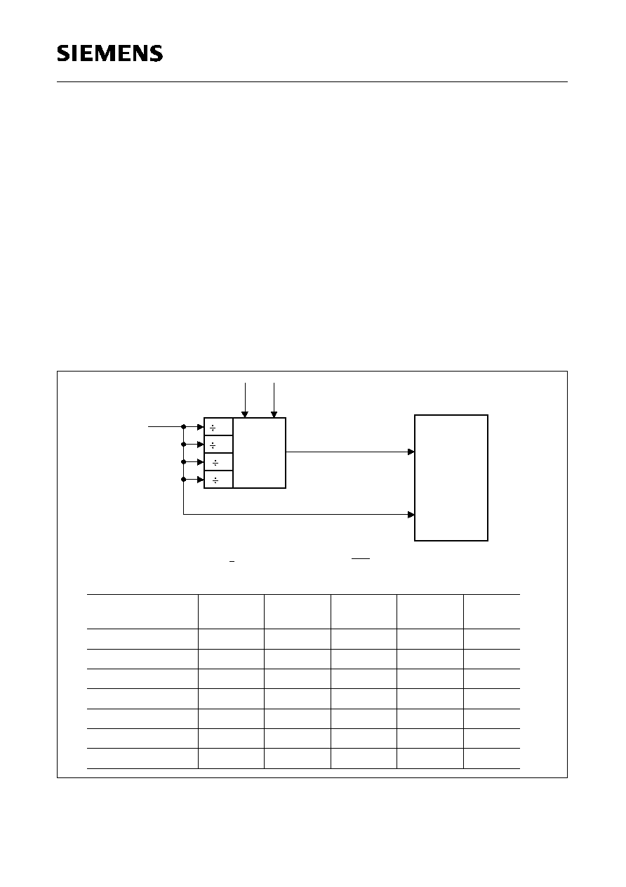
The very first step of the initialization is the CAN controller input clock selection. A divide-by-2
prescaler is enabled by default after reset (figure 16). Setting bit CMOD (SYSCON.3) disables the
prescaler. The purpose of the prescaler selection is:
≠ to ensure that the CAN controller is operable when
f
osc
is over 10 MHz (bit CMOD =0)
≠ to achieve the maximum CAN baudrate of 1 Mbaud when
f
osc
is 8 MHz (bit CMOD=1)
.
Figure 16
CAN Controller Input Clock Selection
Note : The switch configuration shows the reset state of bit CMOD.
Frequency (MHz)
CMOD
(SYSCON.3)
BRP
(BTR0.0-5)
CAN
Baudrate
(Mbaud/sec)
f
OSC
f
CAN
8
8
1
000000B
1
8
4
0
000000B
0.5
16
8
0
000000B
1
SYSCON.3
0
1
(CMOD)
MCS03296
2
f
OSC
Full-CAN
Module
CAN
f
Condition: CMOD = 0, when > 10 MHz
OSC
f
Semiconductor Group
40
1997-12-01
C505 / C505C
C505A / C505CA
8-Bit A/D Converter (C505 and C505C only)
The C505/C505C includes a high performance / high speed 8-bit A/D converter (ADC) with 8 analog
input channels. It operates with a successive approximation technique and provides the following
features:
≠ 8 multiplexed input channels (port 1), which can also be used as digital outputs/inputs
≠ 8-bit resolution
≠ Internal start-of-conversion trigger
≠ Interrupt request generation after each conversion
≠ Single or continuous conversion mode
The 8-bit ADC uses two clock signals for operation : the conversion clock
f
ADC
(=1/
t
ADC
) and the
input clock
f
IN
(1/
t
IN
).
f
ADC
is derived from the C505 system clock
f
OSC
which is applied at the XTAL
pins via the ADC clock prescaler as shown in figure 17. The input clock is equal to
f
OSC
. The
conversion clock
f
ADC
is limited to a maximum frequency of 1.25 MHz. Therefore, the ADC clock
prescaler must be programmed to a value which assures that the conversion clock does not exceed
1.25 MHz. The prescaler ratio is selected by the bits ADCL1 and ADCL0 of SFR ADCON1.
Figure 17
8-Bit A/D Converter Clock Selection
MCU System Clock
Rate (
f
OSC
)
f
IN
[MHz]
Prescaler
Ratio
f
ADC
[MHz]
ADCL1
ADCL0
2 MHz
2
˜
4
0.5
0
0
5 MHz
5
˜
4
1.25
0
0
6 MHz
6
˜
8
0.75
0
1
10 MHz
10
˜
8
1.25
0
1
12 MHz
12
˜
16
0.75
1
0
16 MHz
16
˜
16
1
1
0
20 MHz
20
˜
16
1.25
1
0
MCS03299
f
OSC
MUX
Clock Prescaler
Conversion Clock
Input Clock
f
ADC
IN
f
ADCL1
A / D
Converter
Condition:
ADC max
f
< 1.25 MHz
IN
f
= f
OSC
=
CLP
1
32
8
4
16
ADCL0
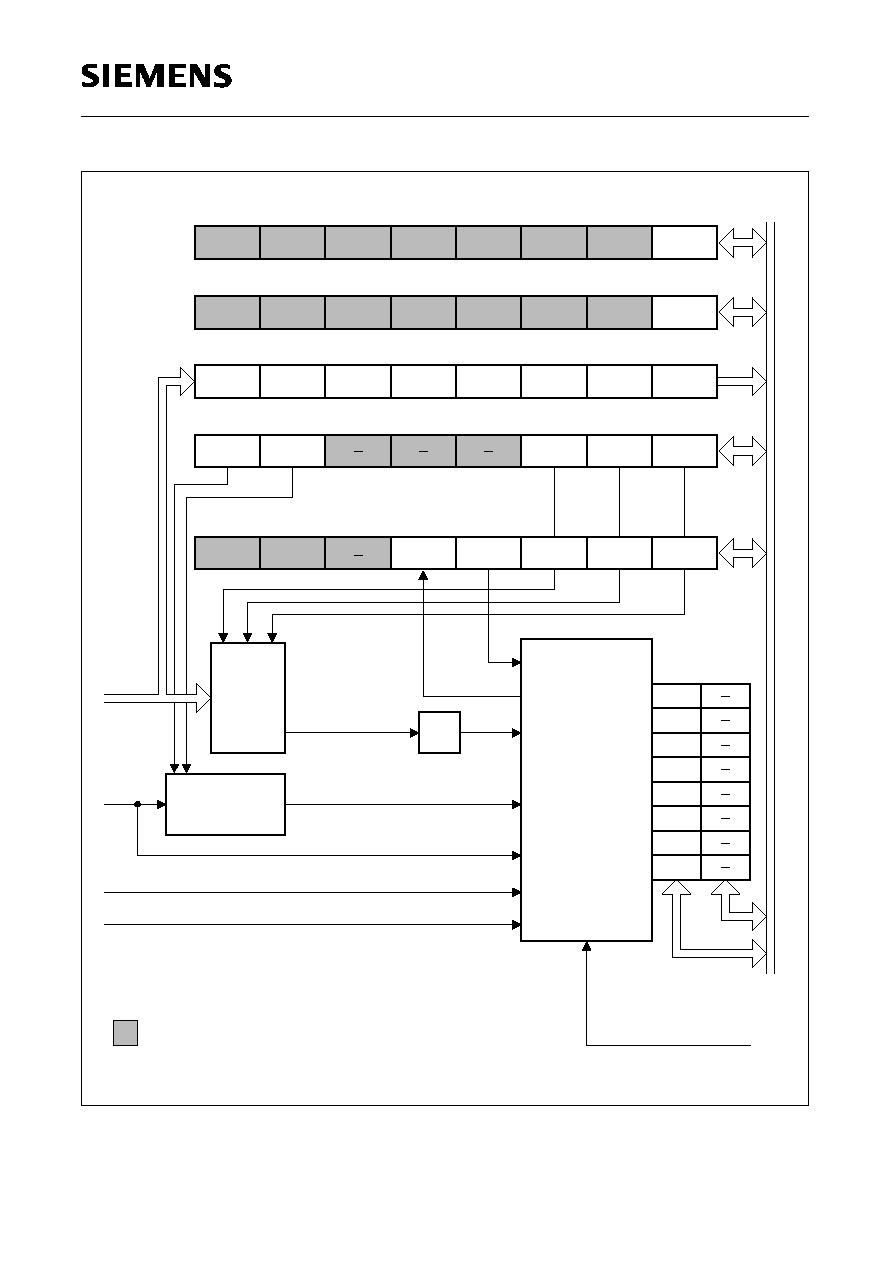
Semiconductor Group
41
1997-12-01
C505 / C505C
C505A / C505CA
Figure 18
Block Diagram of the 8-Bit A/D Converter
C505 / C505C
ADC
Shaded Bit locations are not used in ADC-functions.
f
AGND
AREF
OSC
V
V
Port 1
Conversion
Prescaler
Clock
MUX
f
Conversion Clock
Input Clock
f
IN
S&H
ADCON1 (DC )
ADCON0 (D8 )
ADCL1
H
ADCL0
H
IRCON (C0 )
P1ANA (90 )
EAN7
EAN6
H
H
BSY
EAN5
EAN4
IEN1 (B8 )
H
Write to ADST
MCB03298
(DA )
ADST
conversion
Converter
A / D
Continuous Mode
Single /
Start of
MSB
.6
.5
.4
LSB
.2
.3
.1
H
(D9 )
ADDAT
Bus
Internal
H
ADM
MX2
MX2
EAN3
EAN2
MX1
MX1
MX0
MX0
EAN1
IADC
EAN0
EADC
Bus
Internal
CLK
BD
SWI
IEX3
IEX4
IEX5
IEX6
TF2
EXF2
ECAN
EX3
EX4
EX5
EX6
SWDT
EXEN2
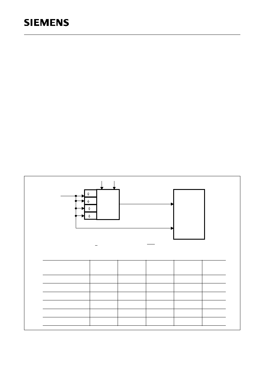
Semiconductor Group
42
1997-12-01
C505 / C505C
C505A / C505CA
10-Bit A/D Converter (C505A and C505CA only)
The C505 includes a high performance / high speed 10-bit A/D-Converter (ADC) with 8 analog input
channels. It operates with a successive approximation technique and uses self calibration
mechanisms for reduction and compensation of offset and linearity errors. The A/D converter
provides the following features:
≠ 8 multiplexed input channels (port 1), which can also be used as digital inputs/outputs
≠ 10-bit resolution
≠ Single or continuous conversion mode
≠ Internal start-of-conversion trigger capability
≠ Interrupt request generation after each conversion
≠ Using successive approximation conversion technique via a capacitor array
≠ Built-in hidden calibration of offset and linearity errors
The 10-bit ADC uses two clock signals for operation : the conversion clock
f
ADC
(=1/
t
ADC
) and the
input clock
f
IN
(=1/
t
IN
). f
ADC
is derived from the C505 system clock
f
OSC
which is applied at the
XTAL pins. The input clock
f
IN
is equal to
f
OSC
The conversion
f
ADC
clock is limited to a maximum
frequency of 2 MHz. Therefore, the ADC clock prescaler must be programmed to a value which
assures that the conversion clock does not exceed 2 MHz. The prescaler ratio is selected by the
bits ADCL1 and ADCL0 of SFR ADCON1.
Figure 19
10-Bit A/D Converter Clock Selection
MCS03635
f
OSC
MUX
Clock Prescaler
Conversion Clock
Input Clock
f
ADC
IN
f
ADCL1
A / D
Converter
Condition:
ADC max
f
< 2 MHz
IN
f
= f
OSC
=
CLP
1
32
8
4
16
ADCL0
MCU System Clock
Rate (
f
OSC
)
f
IN
[MHz]
Prescaler
Ratio
f
ADC
[MHz]
ADCL1
ADCL0
2 MHz
2
˜
4
0.5
0
0
6 MHz
6
˜
4
1.5
0
0
8 MHz
8
˜
4
2
0
0
12 MHz
12
˜
8
1.5
0
1
16 MHz
16
˜
8
2
0
1
20 MHz
20
˜
16
1.25
1
0
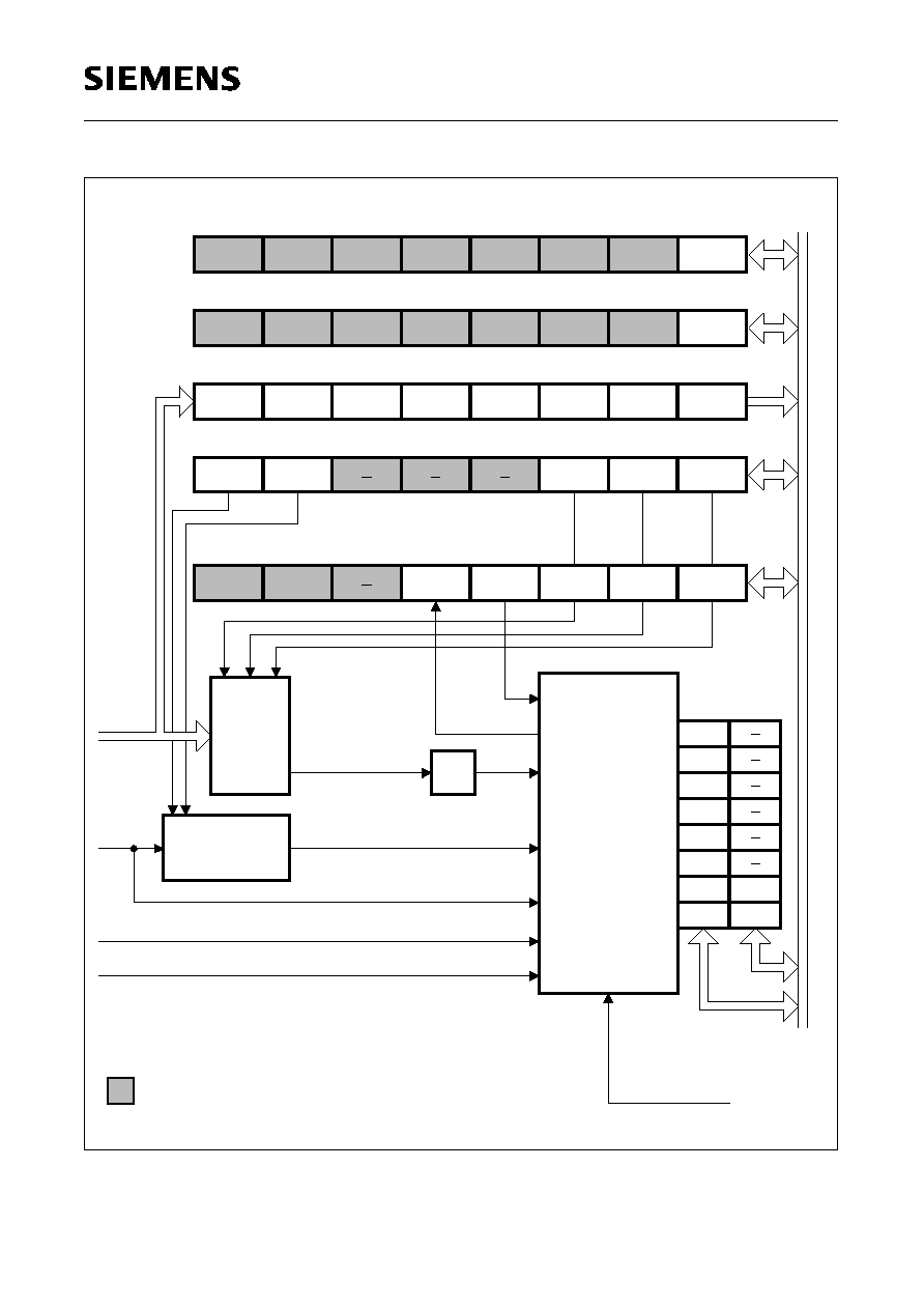
Semiconductor Group
43
1997-12-01
C505 / C505C
C505A / C505CA
Figure 20
Block Diagram of the 10-Bit A/D Converter
ADC
Shaded Bit locations are not used in ADC-functions.
f
AGND
AREF
OSC
V
V
Port 1
Conversion
Prescaler
Clock
MUX
f
Conversion Clock
Input Clock
f
IN
S&H
ADCON1 (DC )
ADCON0 (D8 )
ADCL1
H
ADCL0
H
IRCON (C0 )
P1ANA (90 )
EAN7
EAN6
H
H
BSY
EAN5
EAN4
IEN1 (B8 )
H
Write to ADDATL
MCB03636
(DA )
ADST
conversion
Converter
A / D
Continuous Mode
Single /
Start of
MSB
.6
.5
.4
LSB
.2
.3
.1
H
(D9 )
ADDAT
Bus
Internal
H
ADM
MX2
MX2
EAN3
EAN2
MX1
MX1
MX0
MX0
EAN1
IADC
EAN0
EADC
Bus
Internal
.8
.7
IEX5
EX5
EXF2
EXEN2
BD
CLK
TF2
SWDT
IEX6
EX6
IEX4
EX4
IEX3
EX3
SWI
ECAN
Semiconductor Group
44
1997-12-01
C505 / C505C
C505A / C505CA
Interrupt System
The C505 provides 12 interrupt vectors with four priority levels. Five interrupt requests can be
generated by the on-chip peripherals (timer 0, timer 1, timer 2, serial interface, A/D converter). One
interrupt can be generated by the CAN controller (C505C and C505CA only) or by a software setting
and in this case the interrupt vector is the same. Six interrupts may be triggered externally (P3.2/
INT0, P3.3/INT1, P1.0/AN0/INT3/CC0, P1.1/AN1/INT4/CC1, P1.2/AN2/INT5/CC2, P1.3/AN3/INT6/
CC3). Additionally, the P1.5/AN5/T2EX can trigger an interrupt. The wake-up from power-down
mode interrupt has a special functionality which allows to exit from the software power-down mode
by a short low pulse at either pin P3.2/INT0 or the pin P4.1/RXDC.
Figure 21 to 23 give a general overview of the interrupt sources and illustrate the request and the
control flags which are described in the next sections. Table 10 lists all interrupt sources with their
request flags and interrupt vectior addresses.
Table 10
Interrupt Source and Vectors
Interrupt Source
Interrupt Vector Address
Interrupt Request Flags
External Interrupt 0
0003H
IE0
Timer 0 Overflow
000BH
TF0
External Interrupt 1
0013H
IE1
Timer 1 Overflow
001BH
TF1
Serial Channel
0023H
RI / TI
Timer 2 Overflow / Ext. Reload
002BH
TF2 / EXF2
A/D Converter
0043H
IADC
CAN Controller / Software Interrupt 004BH
≠ / SWI
External interrupt 3
0053H
IEX3
External Interrupt 4
005BH
IEX4
External Interrupt 5
0063H
IEX5
External interrupt 6
006BH
IEX6
Wake-up from power-down mode
007BH
≠
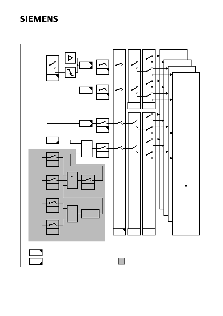
Semiconductor Group
45
1997-12-01
C505 / C505C
C505A / C505CA
Figure 21
Interrupt Structure, Overview Part 1
Note: Each of the 15 CAN controller message objects (C505C and C505CA only), shown in the
shaded area of Figure 21 provides the bits/flags.
2 11 199
EA
ET0
IP1.1
IP0.1
IADC
EADC
EX0
IP1.0
IP0.0
IE0
IEN0.0
TCON.1
0003
H
H
0043
H
000B
H
004B
IEN1.0
IRCON.0
IEN1.1
IEN0.1
A / D Converter
IEN0.7
Highest
Priority Level
Lowest
Priority Level
P
o
l
l
i
n
g
S
e
q
u
e
n
c
e
MCB03303
IT0
TCON.5
TF0
TCON.0
P3.2 /
INT0
Overflow
Timer 0
Bit addressable
Request flag is cleared by hardware
>1
IRCON.1
C505C and C505CA Only
ECAN
SWI
MCR0.5 / 4
MCR0.3 / 2
Receive
Message
Transmit
Message
Error
Status
MCR0.0 / 1
INTPND
CR.1
CR.3
RXIE
TXIE
>1
EIE
CR.2
SIE
>1
IE
CAN Controller Interrupt Sources
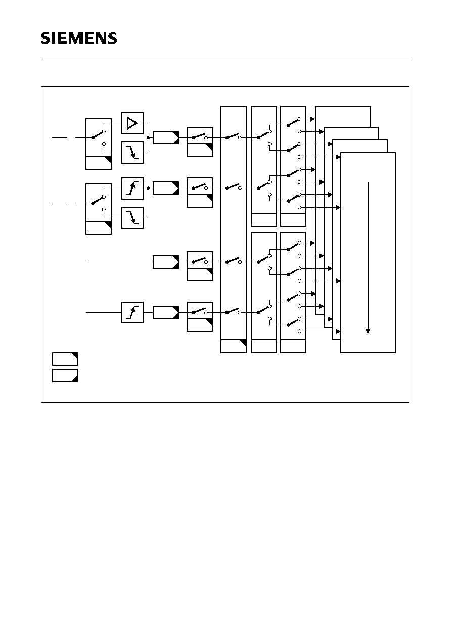
Semiconductor Group
46
1997-12-01
C505 / C505C
C505A / C505CA
Figure 22
Interrupt Structure, Overview Part 2
EA
ET1
IEX3
EX3
EX1
IP1.2
IP0.2
IE1
IEN0.2
TCON.3
0013
H
H
0053
H
001B
H
005B
IEN1.2
IRCON.2
IEN1.3
IEN0.3
IEN0.7
Highest
Priority Level
Lowest
Priority Level
P
o
l
l
i
n
g
S
e
q
u
e
n
c
e
MCB03304
IT1
TCON.7
TF1
TCON.2
P3.3 /
INT1
Overflow
Timer 1
Bit addressable
Request flag is cleared by hardware
AN0 /
INT3 /
T2CON.6
I3FR
P1.0 /
CC0
IP0.3
IP1.3
IRCON.3
IEX4
AN1 /
P1.1 /
INT4 /
CC1
EX4

Semiconductor Group
47
1997-12-01
C505 / C505C
C505A / C505CA
Figure 23
Interrupt Structure, Overview Part 3
EA
ET2
IEX5
EX5
ES
IP1.4
IP0.4
RI
IEN0.4
SCON.0
0023
H
H
0063
H
002B
H
006B
IEN1.4
IRCON.4
IEN1.5
IEN0.5
IEN0.7
Highest
Priority Level
Lowest
Priority Level
P
o
l
l
i
n
g
S
e
q
u
e
n
c
e
MCB03305
USART
Overflow
Timer 2
Bit addressable
Request flag is cleared by hardware
IP0.5
IP1.5
IRCON.5
IEX6
AN2 /
P1.2 /
INT5 /
CC2
EX6
TI
SCON.1
>1
CC3
INT6 /
P1.3 /
IRCON.7
EXF2
TF2
IRCON.6
>1
IEN1.7
EXEN2
AN5 /
T2EX
P1.5 /
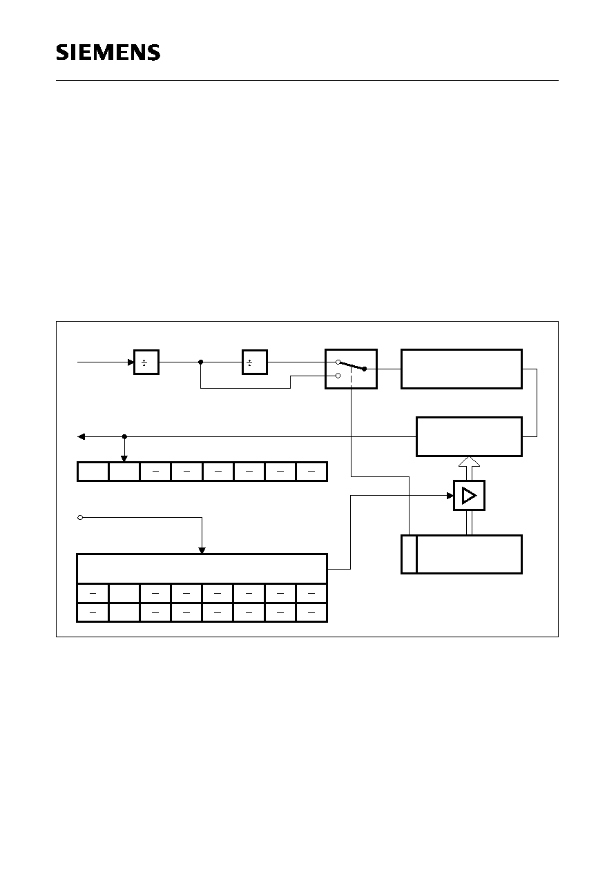
Semiconductor Group
48
1997-12-01
C505 / C505C
C505A / C505CA
Fail Save Mechanisms
The C505 offers enhanced fail safe mechanisms, which allow an automatic recovery from software
upset or hardware failure :
≠ a programmable watchdog timer (WDT), with variable time-out period from 192
µ
s up to
approx. 412.5 ms at 16 MHz.
≠ an oscillator watchdog (OWD) which monitors the on-chip oscillator and forces the
microcontroller into reset state in case the on-chip oscillator fails; it also provides the clock for
a fast internal reset after power-on.
The watchdog timer in the C505 is a 15-bit timer, which is incremented by a count rate of
f
OSC
/12
upto
f
OSC
/192. The system clock of the C505 is divided by two prescalers, a divide-by-two and a
divide-by-16 prescaler. For programming of the watchdog timer overflow rate, the upper 7 bits of the
watchdog timer can be written. Figure 24 shows the block diagram of the watchdog timer unit.
Figure 24
Block Diagram of the Programmable Watchdog Timer
The watchdog timer can be started by software (bit SWDT in SFR IEN1) but it cannot be stopped
during active mode of the device. If the software fails to refresh the running watchdog timer an
internal reset will be initiated on watchdog timer overflow. For refreshing of the watchdog timer the
content of the SFR WDTREL is transfered to the upper 7-bit of the watchdog timer. The refresh
sequence consists of two consequtive instructions which set the bits WDT and SWDT each. The
reset cause (external reset or reset caused by the watchdog) can be examined by software (flag
WDTS). It must be noted, however, that the watchdog timer is halted during the idle mode and
power down mode of the processor.
MCB03306
IP0 (A9 )
H
OSC
f
WDTS
2
16
14
0
7
8
WDTL
WDTH
/ 6
External HW Reset
Control Logic
IEN0 (A8 )
H
IEN1 (B8 )
H
6
7
0
WDT Reset - Request
WDTPSEL
WDTREL (86 )
H
WDT
SWDT
OWDS

Semiconductor Group
49
1997-12-01
C505 / C505C
C505A / C505CA
Oscillator Watchdog
The oscillator watchdog unit serves for three functions:
≠ Monitoring of the on-chip oscillator's function
The watchdog supervises the on-chip oscillator's frequency; if it is lower than the frequency
of the auxiliary RC oscillator in the watchdog unit, the internal clock is supplied by the RC
oscillator and the device is brought into reset; if the failure condition disappears (i.e. the
on-chip oscillator has a higher frequency than the RC oscillator), the part, in order to allow the
oscillator to stabilize, executes a final reset phase of typ. 1 ms; then the oscillator watchdog
reset is released and the part starts program execution from address 0000H again.
≠ Fast internal reset after power-on
The oscillator watchdog unit provides a clock supply for the reset before the on-chip oscillator
has started. The oscillator watchdog unit also works identically to the monitoring function.
≠ Control of external wake-up from software power-down mode
When the power-down mode is left by a low level at the P3.2/INT0 pin or the P4.1/RXDC pin,
the oscillator watchdog unit assures that the microcontroller resumes operation (execution of
the power-down wake-up interrupt) with the nominal clock rate. In the power-down mode the
RC oscillator and the on-chip oscillator are stopped. Both oscillators are started again when
power-down mode is released. When the on-chip oscillator has a higher frequency than the
RC oscillator, the microcontroller starts program execution by processing a power down
interrupt after a final delay of typ. 1 ms in order to allow the on-chip oscillator to stabilize.
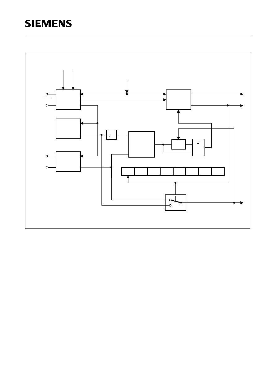
Semiconductor Group
50
1997-12-01
C505 / C505C
C505A / C505CA
Figure 25
Functional Block Diagram of the Oscillator Watchdog
Int. Clock
XTAL2
XTAL1
OWDS
MCB03308
IP0 (A9 )
H
3 MHz
f
RC
Delay
1
f
2
f
2
f
1
f
<
P4.1 / RXDC
Start /
Stop
Start /
Stop
Mode Activated
Power - Down
Power-Down Mode
Wake - Up Interrupt
Internal Reset
10
P3.2 / INT0
Control
WS
(PCON1.4)
(PCON1.7)
EWPD
>1
Frequency
Comparator
RC
On-Chip
Oscillator
Logic
Oscillator
Logic
Control

Semiconductor Group
51
1997-12-01
C505 / C505C
C505A / C505CA
Power Saving Modes
The C505 provides two basic power saving modes, the idle mode and the power down mode.
Additionally, a slow down mode is available. This power saving mode reduces the internal clock rate
in normal operating mode and it can be also used for further power reduction in idle mode.
≠ Idle mode
In the idle mode the main oscillator of the C505 continues to run, but the CPU is gated off from
the clock signal. All peripheral units are further provided with the clock. The CPU status is
preserved in its entirety. The idle mode can be terminated by any enabled interrupt of a
peripheral unit or by a hardware reset.
≠ Power down mode
The operation of the C505 is completely stopped and the oscillator is turned off. This mode is
used to save the contents of the internal RAM with a very low standby current. Power down
mode is entered by software and can be left by reset or by a short low pulse at pin P3.2/
INT0.or P4.1/RXDC.
≠ Slow down mode
The controller keeps up the full operating functionality, but its normal clock frequency is
internally divided by 32. This slows down all parts of the controller, the CPU and all
peripherals, to 1/32-th of their normal operating frequency. Slowing down the frequency
significantly reduces power consumption.
In the power down mode of operation,
V
CC
can be reduced to minimize power consumption. It must
be ensured, however, that
V
CC
is not reduced before the power down mode is invoked, and that
V
CC
is restored to its normal operating level, before the power down mode is terminated. Table 11 gives
a general overview of the entry and exit procedures of the power saving modes.
Table 11
Power Saving Modes Overview
Mode
Entering
(Instruction
Example)
Leaving by
Remarks
Idle Mode
ORL PCON, #01H
ORL PCON, #20H
Ocurrence of an
interrupt from a
peripheral unit
CPU clock is stopped;
CPU maintains their data;
peripheral units are active (if
enabled) and provided with
clock
Hardware Reset
Power Down Mode
ORL PCON, #02H
ORL PCON, #40H
Hardware Reset
Oscillator is stopped;
contents of on-chip RAM and
SFR's are maintained;
Short low pulse at
pin P3.2/INT0 or
P4.1/RXDC
Slow Down Mode
ORL PCON,#10H
ANL PCON,#0EFH
or
Hardware Reset
Oscillator frequency is
reduced to 1/32 of its nominal
frequency
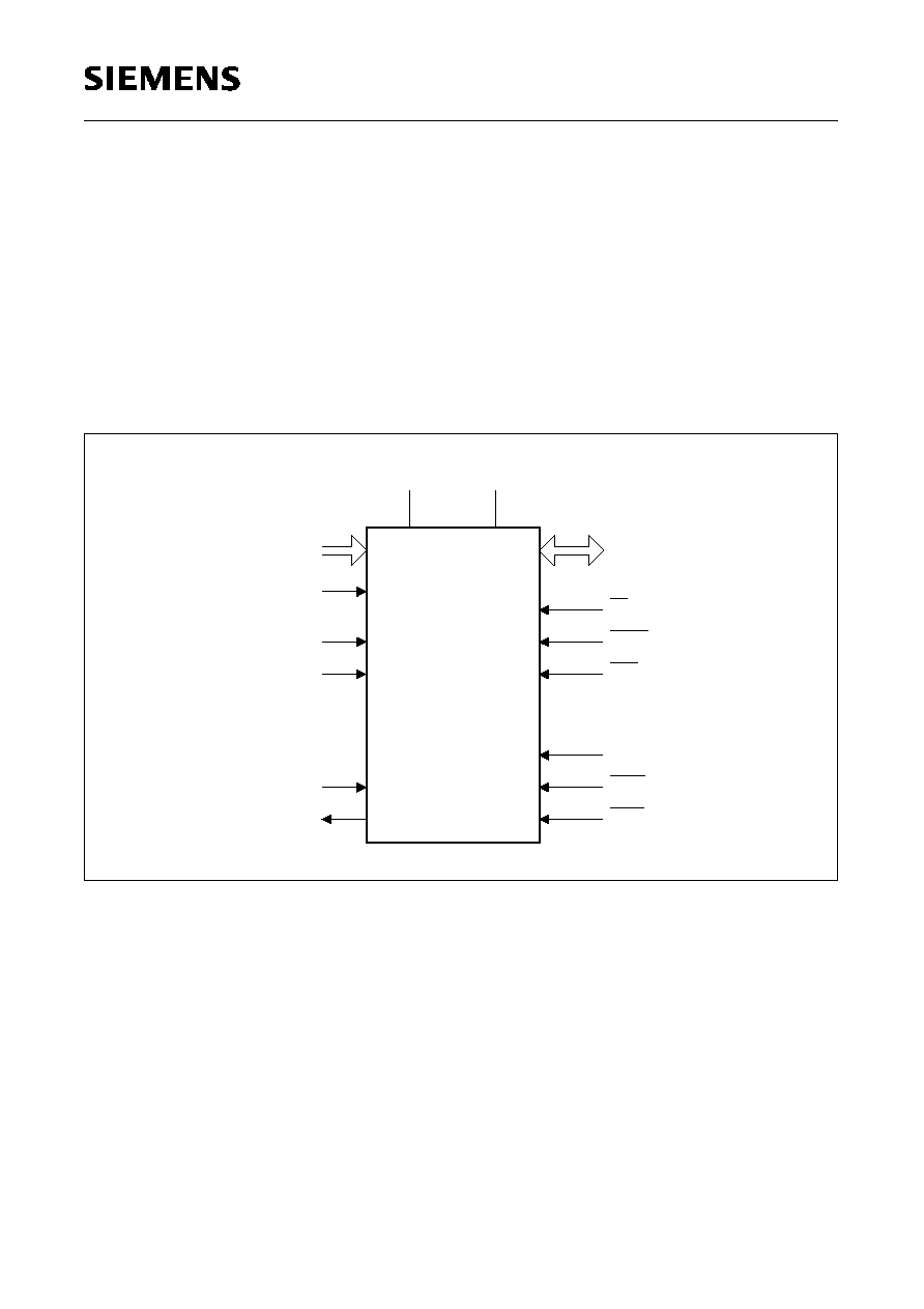
Semiconductor Group
52
1997-12-01
C505 / C505C
C505A / C505CA
OTP Memory Operation (C505A and C505CA only)
The C505A/C505CA contains a 32k byte one-time programmable (OTP) program memory. With the
C505A/C505CA fast programming cycles are achieved (1 byte in 100
µ
sec). Also several levels of
OTP memory protection can be selected.
For programming of the device, the C505A/C505CA must be put into the programming mode. This
typically is done not in-system but in a special programming hardware. In the programming mode
the C505A/C505CA operates as a slave device similar as an EPROM standalone memory device
and must be controlled with address/data information, control lines, and an external 11.5V
programming voltage. Figure 26 shows the pins of the C505A/C505CA which are required for
controlling of the OTP programming mode.
Figure 26
Programming Mode Configuration
PMSEL1
PMSEL0
XTAL2
XTAL1
D0 - D7
V
SS
V
CC
C505A
MCS03637
PALE
EA /
PROG
PRD
RESET
PSEN
PSEL
V
PP
Port 2
Port 0
A0 - A7 /
A8 - A14
C505CA
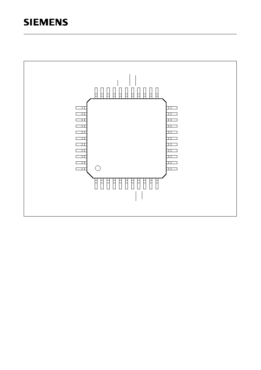
Semiconductor Group
53
1997-12-01
C505 / C505C
C505A / C505CA
Pin Configuration in Programming Mode
Figure 27
P-MQFP-44 Pin Configuration of the C505A/C505CA in Programming Mode (Top View)
EA /
N.C.
D6
D7
D5
A6 / A14
A5 / A13
PSEN
A7
PROG
A4 / A12
A3 / A11
XTAL2
XTAL1
N.C.
N.C.
PSEL
PRD
RESET
N.C.
N.C.
11
1
6
34
39
44
16
21
22
MCP03638
A2 / A10
A1 / A9
V
V
CC
SS
A0 / A8
33
31 30 29 28 27 26 25 24 23
32
D4
PMSEL0
PALE
N.C.
PMSEL1
N.C.
2 3 4 5
7 8
10
9
20
19
18
17
15
14
13
12
43
42
41
40
38
37
36
35
C505A
D3
D2
D1
D0
N.C.
N.C.
C505CA
PP
V
N.C.
N.C.
N.C.
N.C.
N.C.
N.C.
Semiconductor Group
54
1997-12-01
C505 / C505C
C505A / C505CA
The following table 12 contains the functional description of all C505A/C505CA pins which are
required for OTP memory programming.
Table 12
Pin Definitions and Functions in Programming Mode
Symbol
Pin Number
I/O
*)
Function
RESET
4
I
Reset
This input must be at static "1" (active) level during the whole
programming mode.
PMSEL0
PMSEL1
5
7
I
I
Programming mode selection pins
These pins are used to select the different access modes in
programming mode. PMSEL1,0 must satisfy a setup time to the
rising edge of PALE. When the logic level of PMSEL1,0 is
changed, PALE must be at low level.
PSEL
8
I
Basic programming mode select
This input is used for the basic programming mode selection
and must be switched according figure 3-1.
PRD
9
I
Programming mode read strobe
This input is used for read access control for OTP memory
read, Version Register read, and lock bit read operations.
PALE
10
I
Programming address latch enable
PALE is used to latch the high address lines. The high address
lines must satisfy a setup and hold time to/from the falling edge
of PALE. PALE must be at low level when the logic level of
PMSEL1,0 is changed.
XTAL2
14
O
XTAL2
Output of the inverting oscillator amplifier.
XTAL1
15
I
XTAL1
Input to the oscillator amplifier.
V
SS
16
≠
Circuit ground potential
must be applied in programming mode.
V
CC
17
≠
Power supply terminal
must be applied in programming mode.
*) I = Input
O = Output
PMSEL1
PMSEL0
Access Mode
0
0
Reserved
0
1
Read version bytes
1
0
Program/read lock bits
1
1
Program/read OTP memory byte
Semiconductor Group
55
1997-12-01
C505 / C505C
C505A / C505CA
P2.0-7
18-25
I
Address lines
P2.0-7 are used as multiplexed address input lines A0-A7 and
A8-A14. A8-A14 must be latched with PALE.
PSEN
26
I
Program store enable
This input must be at static "0" level during the whole
programming mode.
PROG
27
I
Programming mode write strobe
This input is used in programming mode as a write strobe for
OTP memory program, and lock bit write operations During
basic programming mode selection a low level must be applied
to PROG.
EA/V
PP
29
≠
External Access / Programming voltage
This pin must be at 11.5V (V
PP
) voltage level during
programming of an OTP memory byte or lock bit. During an
OTP memory read operation this pin must be at V
IH
high level.
This pin is also used for basic programming mode selection. At
basic programming mode selection a low level must be applied
to EA/V
PP
.
D7-0
30-37
I/O
Data lines 0-7
During programming mode, data bytes are transferred via the
bidirectional port 0 data lines.
N.C.
1-3, 6, 11-13,
28, 38-44
≠
Not Connected
These pins should not be connected in programming mode.
*) I = Input
O = Output
Table 12
Pin Definitions and Functions in Programming Mode (cont'd)
Symbol
Pin Number
I/O
*)
Function
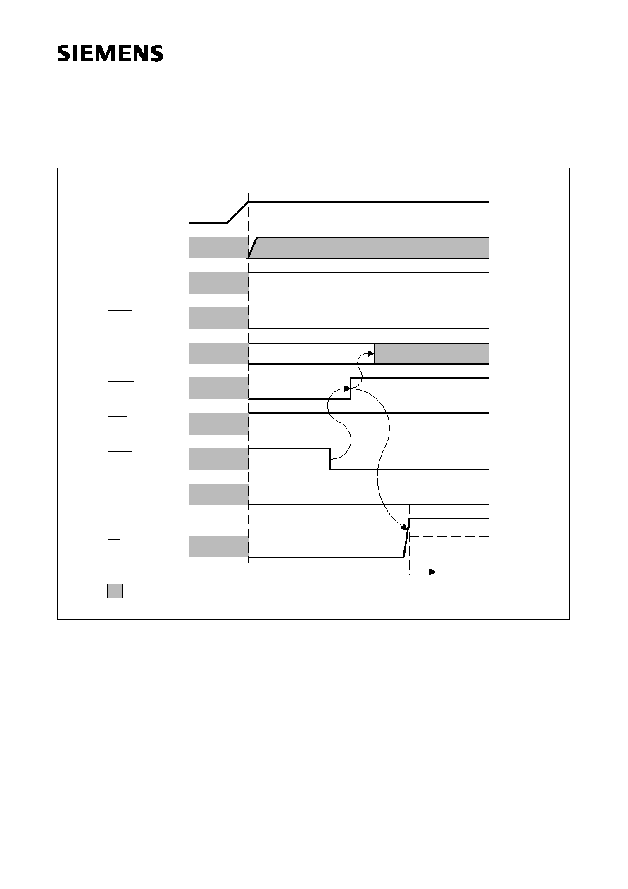
Semiconductor Group
56
1997-12-01
C505 / C505C
C505A / C505CA
Basic Programming Mode Selection
The basic programming mode selection scheme is shown in figure 28.
Figure 28
Basic Programming Mode Selection
Clock
(XTAL1 / XTAL2)
RESET
PSEN
PMSEL1,0
PROG
PRD
PSEL
PALE
EA /
V
PP
V
CC
5 V
V
PP
IH
V
"1"
"0"
0,1
"0"
"1"
"0"
0 V
Ready for access
mode selection
During this period signals
are not actively driven
MCS03639
Stable
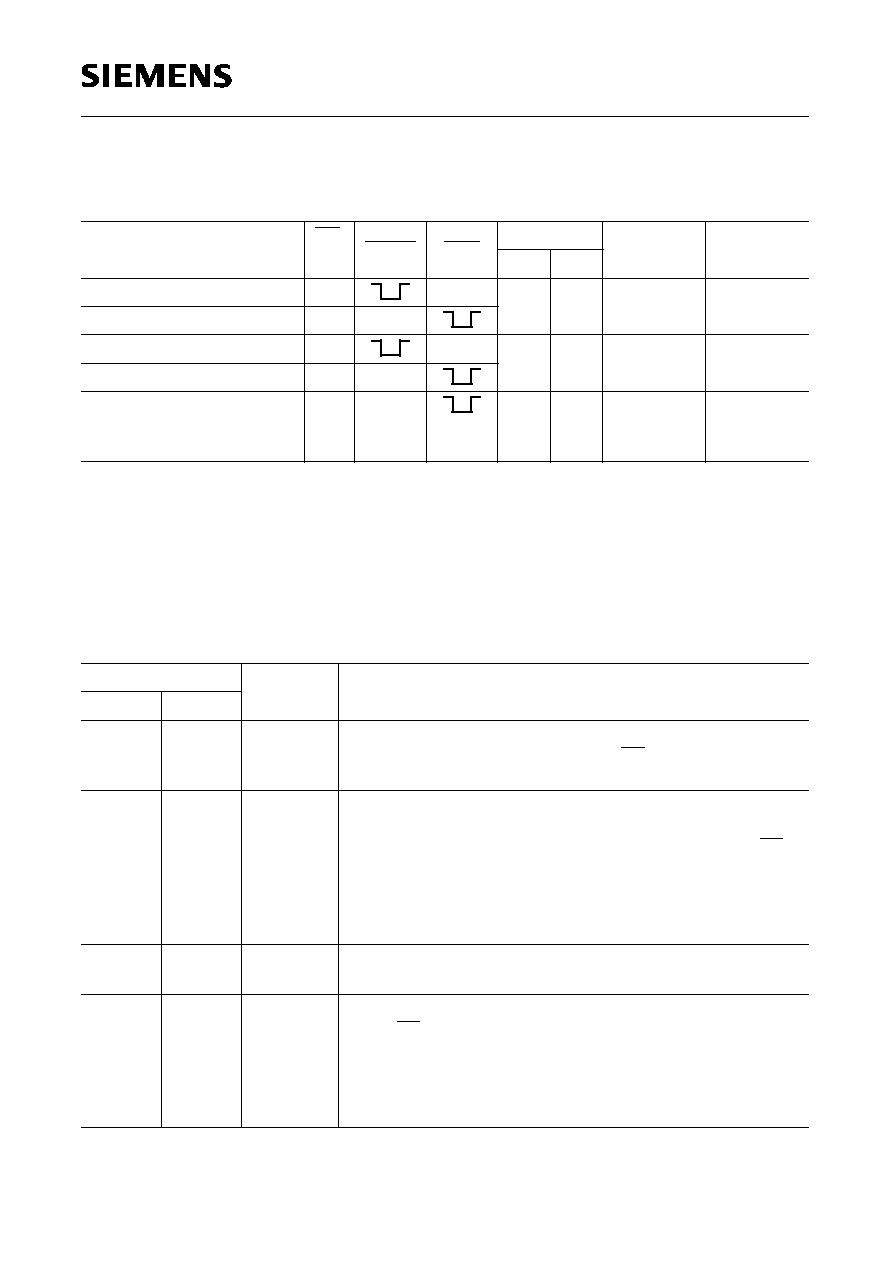
Semiconductor Group
57
1997-12-01
C505 / C505C
C505A / C505CA
Lock Bits Programming / Read
The C505A/C505CA has two programmable lock bits which, when programmed according table 14,
provide four levels of protection for the on-chip OTP code memory. The state of the lock bits can
also be read.
Table 13
Access Modes Selection
Access Mode
EA/
V
PP
PROG
PRD
PMSEL
Address
(Port 2)
Data
(Port 0)
1
0
Program OTP memory byte
V
PP
H
H
H
A0-7
A8-14
D0-7
Read OTP memory byte
V
IH
H
Program OTP lock bits
V
PP
H
H
L
≠
D1,D0 see
table 14
Read OTP lock bits
V
IH
H
Read OTP version byte
V
IH
H
L
H
Byte addr.
of version
byte
D0-7
Table 14
Lock Bit Protection Types
Lock Bits at D1,D0
Protection
Level
Protection Type
D1
D0
1
1
Level 0
The OTP lock feature is disabled. During normal operation of
the C505A/C505CA, the state of the EA pin is not latched on
reset.
1
0
Level 1
During normal operation of the C505A/C505CA, MOVC
instructions executed from external program memory are
disabled from fetching code bytes from internal memory. EA is
sampled and latched on reset. An OTP memory read operation
is only possible using the ROM/OTP verification mode 2 for
protection level 1. Further programming of the OTP memory is
disabled (reprogramming security).
0
1
Level 2
Same as level 1, but also OTP memory read operation using
OTP verification mode is disabled.
0
0
Level 3
Same as level 2; but additionally external code execution by
setting EA=low during normal operation of the C505A/C505CA
is no more possible.
External code execution, which is initiated by an internal
program (e.g. by an internal jump instruction above the ROM
boundary), is still possible.

Semiconductor Group
58
1997-12-01
C505 / C505C
C505A / C505CA
Absolute Maximum Ratings
Ambient temperature under bias (
T
A
) ......................................................... ≠ 40
∞
C to 125
∞
C
Storage temperature (
T
stg
) .......................................................................... ≠ 65
∞
C to 150
∞
C
Voltage on
V
CC
pins with respect to ground (
V
SS
) ....................................... ≠ 0.5 V to 6.5 V
Voltage on any pin with respect to ground (
V
SS
) ......................................... ≠ 0.5 V to
V
CC
+0.5 V
Input current on any pin during overload condition..................................... ≠ 10 mA to 10 mA
Absolute sum of all input currents during overload condition ..................... I 100 mA I
Power dissipation........................................................................................ TBD
Note: Stresses above those listed under "Absolute Maximum Ratings" may cause permanent
damage of the device. This is a stress rating only and functional operation of the device at
these or any other conditions above those indicated in the operational sections of this
specification is not implied. Exposure to absolute maximum rating conditions for longer
periods may affect device reliability. During overload conditions (
V
IN
>
V
CC
or
V
IN
<
V
SS
) the
Voltage on
V
CC
pins with respect to ground (
V
SS
) must not exceed the values defined by the
absolute maximum ratings.
Semiconductor Group
59
1997-12-01
C505 / C505C
C505A / C505CA
DC Characteristics
V
CC
= 5 V + 10%, ≠ 15%;
V
SS
= 0 V
T
A
= 0 to 70
∞
C for the SAB- versions
T
A
= ≠ 40 to 85
∞
C for the SAF- versions
T
A
= ≠ 40 to 110
∞
C for the SAH- versions
T
A
= ≠ 40 to 125
∞
C for the SAK- versions
Notes see next but one page 61
Parameter
Symbol
Limit Values
Unit
Test Condition
min.
max.
Input low voltages
all except EA, RESET
EA pin
RESET pin
V
IL
V
IL1
V
IL2
≠ 0.5
≠ 0.5
≠ 0.5
0.2
V
CC
- 0.1
0.2
V
CC
- 0.3
0.2
V
CC
+ 0.1
V
V
V
≠
≠
≠
Input high voltages
all except XTAL1, RESET
XTAL1 pin
RESET pin
V
IH
V
IH1
V
IH2
0.2
V
CC
+ 0.9
0.7
V
CC
0.6
V
CC
V
CC
+ 0.5
V
CC
+ 0.5
V
CC
+ 0.5
V
V
V
≠
≠
≠
Output low voltages
Ports 1, 2, 3, 4
Port 0, ALE, PSEN
V
OL
V
OL1
≠
≠
0.45
0.45
V
V
I
OL
= 1.6 mA
1)
I
OL
= 3.2 mA
1)
Output high voltages
Ports 1, 2, 3, 4
Port 0 in external bus mode,
ALE, PSEN
V
OH
V
OH2
2.4
0.9
V
CC
2.4
0.9
V
CC
≠
≠
≠
≠
V
V
V
V
I
OH
= ≠ 80
µ
A
I
OH
= ≠ 10
µ
A
)
I
OH
= ≠ 800
µ
A
I
OH
= ≠ 80
µ
A
2)
Logic 0 input current
Ports 1, 2, 3, 4
I
IL
≠ 10
≠ 70
µ
A
V
IN
= 0.45 V
Logical 0-to-1 transition current
Ports 1, 2, 3, 4
I
TL
≠ 65
≠ 650
µ
A
V
IN
= 2 V
Input leakage current
Port 0, AN0-7 (Port 1), EA
I
LI
≠
±
1
µ
A
0.45 <
V
IN
<
V
CC
Pin capacitance
C
IO
≠
10
pF
f
c
1 MHz,
T
A
= 25
∞
C
Overload current
I
OV
≠
±
5
mA
3) 4)
Programming voltage
V
PP
10.9
12.1
V
11.5 V
±
5%
5)
Supply current at EA/
V
CC
30
mA
5) 6)
Semiconductor Group
60
1997-12-01
C505 / C505C
C505A / C505CA
Power Supply Currents
Notes see next page 61
Parameter
Symbol
Limit Values
Unit Test Condition
typ.
12)
max.
13)
C505 /
C505C
Active Mode
12 MHz
20 MHz
I
CC
I
CC
19.7
32
TBD
TBD
mA
7)
Idle Mode
12 MHz
20 MHz
I
CC
I
CC
11.7
17.8
TBD
TBD
mA
8)
Active Mode with
slow-down enabled
12 MHz
20 MHz
I
CC
I
CC
4.4
4.9
TBD
TBD
mA
9)
Idle Mode with
slow-down enabled
12 MHz
20 MHz
I
CC
I
CC
3.6
4.0
TBD
TBD
mA
10)
Power down current
I
PD
7
TBD
µ
A
V
CC
= 2..5.5 V
11)
C505A
C505CA
Active Mode
12 MHz
20 MHz
I
CC
I
CC
18.2
28.8
TBD
TBD
mA
7)
Idle Mode
12 MHz
20 MHz
I
CC
I
CC
9.4
14.1
TBD
TBD
mA
8)
Active Mode with
slow-down enabled
12 MHz
20 MHz
I
CC
I
CC
3.5
4.2
TBD
TBD
mA
9)
Idle Mode with
slow-down enabled
12 MHz
20 MHz
I
CC
I
CC
3.0
3.4
TBD
TBD
mA
10)
Power down current
I
PD
40
TBD
µ
A
V
CC
= 2..5.5 V
11)

Semiconductor Group
61
1997-12-01
C505 / C505C
C505A / C505CA
Notes:
1) Capacitive loading on ports 0 and 2 may cause spurious noise pulses to be superimposed on the
V
OL
of ALE
and port 3. The noise is due to external bus capacitance discharging into the port 0 and port 2 pins when these
pins make 1-to-0 transitions during bus operation. In the worst case (capacitive loading > 100 pF), the noise
pulse on ALE line may exceed 0.8 V. In such cases it may be desirable to qualify ALE with a schmitt-trigger,
or use an address latch with a schmitt-trigger strobe input.
2) Capacitive loading on ports 0 and 2 may cause the
V
OH
on ALE and PSEN to momentarily fall below the
0.9
V
CC
specification when the address lines are stabilizing.
3) Overload conditions occur if the standard operating conditions are exceeded, ie. the voltage on any pin
exceeds the specified range (i.e.
V
OV
>
V
CC
+ 0.5 V or
V
OV
<
V
SS
- 0.5 V). The supply voltage
V
CC
and
V
SS
must
remain within the specified limits. The absolute sum of input currents on all port pins may not exceed 50 mA.
4) Not 100% tested, guaranteed by design characterization.
5) Only valid for C505A and C505CA.
6) Only valid for C505A and C505CA in programming mode.
7)
I
CC
(active mode) is measured with:
XTAL1 driven with
t
R
,
t
F
= 5 ns, 50% duty cycle ,
V
IL
=
V
SS
+ 0.5 V,
V
IH
=
V
CC
≠ 0.5 V; XTAL2 = N.C.;
EA = Port 0 = RESET =
V
CC
; all other pins are disconnected.
8)
I
CC
(idle mode) is measured with all output pins disconnected and with all peripherals disabled;
XTAL1 driven with
t
R
,
t
F
= 5 ns, 50% duty cycle,
V
IL
=
V
SS
+ 0.5 V,
V
IH
=
V
CC
≠ 0.5 V; XTAL2 = N.C.;
RESET = EA =
V
SS
; Port0 =
V
CC
; all other pins are disconnected;
9)
I
CC
(active mode with slow-down mode) is measured : TBD
10)
I
CC
(idle mode with slow-down mode) is measured : TBD
11)
I
PD
(power-down mode) is measured under following conditions:
EA = Port 0 =
V
CC
; RESET =
V
SS
; XTAL2 = N.C.; XTAL1 =
V
SS
;
V
AGND
=
V
SS
;
V
AREF
=
V
CC
;
all other pins are disconnected.
12) The typical
I
CC
values are periodically measured at
T
A
= + 25
∞
C but not 100% tested.
13) The maximum
I
CC
values are measured under worst case conditions (
T
A
= 0
∞
C or ≠ 40
∞
C and
V
CC
= 5.5 V)

Semiconductor Group
62
1997-12-01
C505 / C505C
C505A / C505CA
Figure 29
ICC Diagram of C505 and C505C
C505/C505C: Power Supply Current Calculation Formulas
Note:
f
osc
is the oscillator frequency in MHz.
I
CC
values are given in mA.
Parameter
Symbol
Formula
Active mode
I
CC typ
I
CC max
TBD
TBD
Idle mode
I
CC typ
I
CC max
TBD
TBD
Active mode with
slow-down enabled
I
CC typ
I
CC max
TBD
TBD
Idle mode with
slow-down enabled
I
CC typ
I
CC max
TBD
TBD
CC
0
0
OSC
f
MCD03640
MHz
20
mA
CC max
CC typ
4
8
12
18
5
10
15
20
25
30
TBD
Semiconductor Group
63
1997-12-01
C505 / C505C
C505A / C505CA
Figure 30
ICC Diagram of C505A and C505CA
C505A : Power Supply Current Calculation Formulas
Note:
f
osc
is the oscillator frequency in MHz.
I
CC
values are given in mA.
Parameter
Symbol
Formula
Active mode
I
CC typ
I
CC max
TBD
TBD
Idle mode
I
CC typ
I
CC max
TBD
TBD
Active mode with
slow-down enabled
I
CC typ
I
CC max
TBD
TBD
Idle mode with
slow-down enabled
I
CC typ
I
CC max
TBD
TBD
CC
0
0
OSC
f
MCD03641
MHz
20
mA
CC max
CC typ
4
8
12
18
5
10
15
20
25
30
TBD
Semiconductor Group
64
1997-12-01
C505 / C505C
C505A / C505CA
A/D Converter Characteristics of C505 and C505C
V
CC
= 5 V + 10%, ≠ 15%;
V
SS
= 0 V
T
A
= 0 to 70
∞
C for the SAB- versions
T
A
= ≠ 40 to 85
∞
C for the SAF- versions
T
A
= ≠ 40 to 110
∞
C for the SAH- versions
T
A
= ≠ 40 to 125
∞
C for the SAK- versions
4 V
V
AREF
V
CC
+
0.1 V;
V
SS
≠
0.1 V
V
AGND
V
SS
+ 0.2 V
Notes see next page.
Clock calculation table:
Further timing conditions :
t
ADC
min = 800 ns
t
IN
= 1 /
f
OSC
=
t
CLP
Parameter
Symbol
Limit Values
Unit
Test Condition
min.
max.
Analog input voltage
V
AIN
V
AGND
-
0.2
V
AREF
+
0.2
V
1)
Sample time
t
S
≠
64
◊
t
IN
32
◊
t
IN
16
◊
t
IN
8
◊
t
IN
ns
Prescaler
˜
32
Prescaler
˜
16
Prescaler
˜
8
Prescaler
˜
4
2)
Conversion cycle time
t
ADCC
≠
320
◊
t
IN
160
◊
t
IN
80
◊
t
IN
40
◊
t
IN
ns
Prescaler
˜
32
Prescaler
˜
16
Prescaler
˜
8
Prescaler
˜
4
3)
Total unadjusted error
T
UE
≠
±
2
LSB
V
SS
+ 0.5 V
V
AIN
V
CC
≠ 0.5 V
4)
Internal resistance of
reference voltage source
R
AREF
≠
t
ADC
/ 500
- 1
k
t
ADC
in [ns]
5) 6)
Internal resistance of
analog source
R
ASRC
≠
t
S
/ 500
- 1
k
t
S
in [ns]
2) 6)
ADC input capacitance
C
AIN
≠
50
pF
6)
Clock Prescaler
Ratio
ADCL1, 0
t
ADC
t
S
t
ADCC
˜
32
1 1
32
◊
t
IN
64
◊
t
IN
320
◊
t
IN
˜
16
1 0
16
◊
t
IN
32
◊
t
IN
160
◊
t
IN
˜
8
0 1
8
◊
t
IN
16
◊
t
IN
80
◊
t
IN
˜
4
0 0
4
◊
t
IN
8
◊
t
IN
40
◊
t
IN

Semiconductor Group
65
1997-12-01
C505 / C505C
C505A / C505CA
Notes:
1)
V
AIN
may exeed
V
AGND
or
V
AREF
up to the absolute maximum ratings. However, the conversion result in
these cases will be 00
H
or FF
H
, respectively.
2) During the sample time the input capacitance
C
AIN
must be charged/discharged by the external source. The
internal resistance of the analog source must allow the capacitance to reach their final voltage level within
t
S
.
After the end of the sample time
t
S
, changes of the analog input voltage have no effect on the conversion
result.
3) This parameter includes the sample time
t
S
, the time for determining the digital result. Values for the
conversion clock
t
ADC
depend on programming and can be taken from the table on the previous page.
4) T
UE
(max.) is tested at ≠ 40
T
A
125
∞
C;
V
CC
5.5 V;
V
AREF
V
CC
+ 0.1 V and
V
SS
V
AGND
. It is
guaranteed by design characterization for all other voltages within the defined voltage range.
If an overload condition occurs on maximum 2 unused analog input pins and the absolute sum of input
overload currents on all analog input pins does not exceed 10 mA, an additional conversion error of 1/2 LSB
is permissible.
5) During the conversion the ADC's capacitance must be repeatedly charged or discharged. The internal
resistance of the reference source must allow the capacitance to reach their final voltage level within the
indicated time. The maximum internal resistance results from the programmed conversion timing.
6) Not 100% tested, but guaranteed by design characterization.
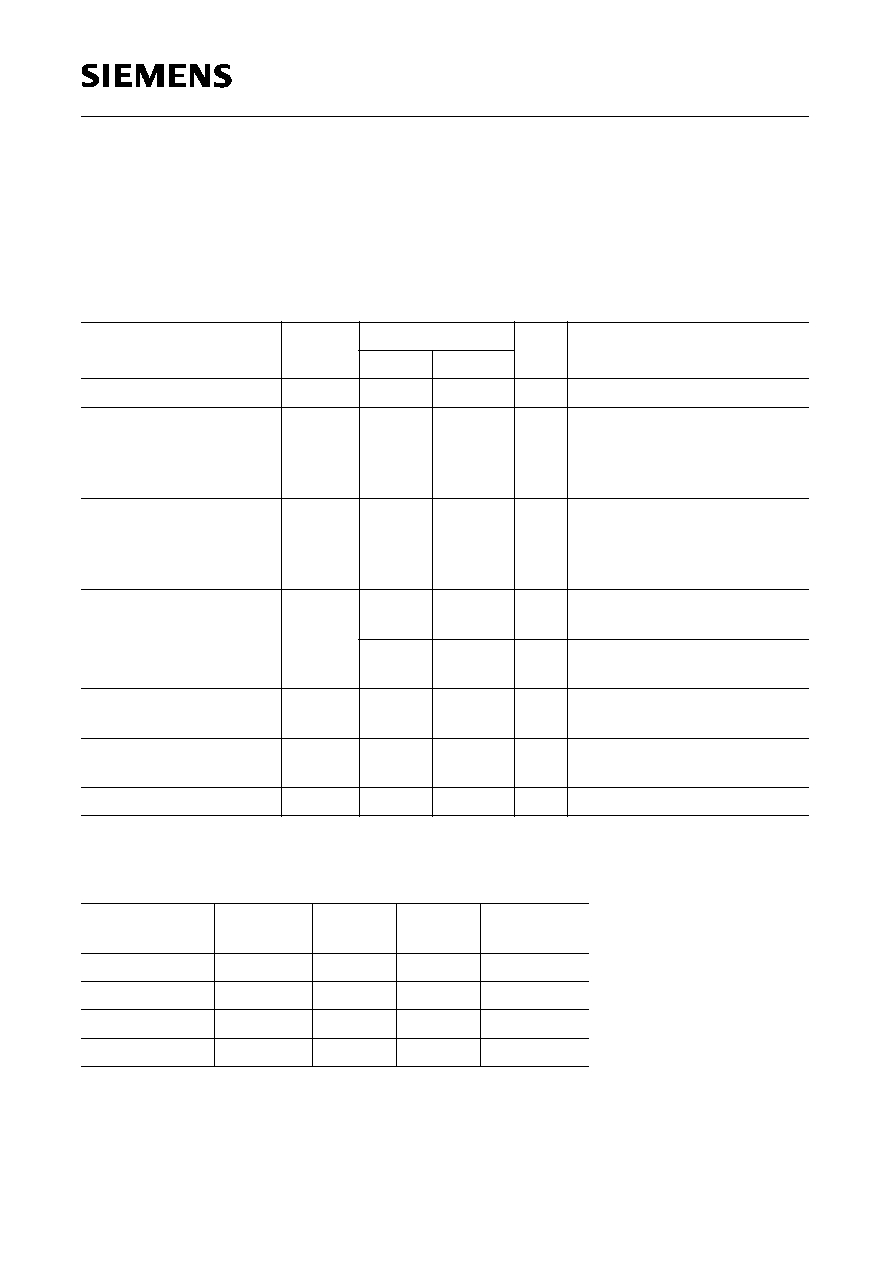
Semiconductor Group
66
1997-12-01
C505 / C505C
C505A / C505CA
A/D Converter Characteristics of C505A and C505CA
V
CC
= 5 V + 10%, ≠ 15%;
V
SS
= 0 V
T
A
= 0 to 70
∞
C for the SAB- versions
T
A
= ≠ 40 to 85
∞
C for the SAF- versions
T
A
= ≠ 40 to 110
∞
C for the SAH- versions
T
A
= ≠ 40 to 125
∞
C for the SAK- versions
4 V
V
AREF
V
CC
+
0.1 V;
V
SS
≠
0.1 V
V
AGND
V
SS
+ 0.2 V
Notes see next page.
Clock calculation table:
Further timing conditions :
t
ADC
min = 500 ns
t
IN
= 1 /
f
OSC
=
t
CLP
Parameter
Symbol
Limit Values
Unit
Test Condition
min.
max.
Analog input voltage
V
AIN
V
AGND
V
AREF
V
1)
Sample time
t
S
≠
64
◊
t
IN
32
◊
t
IN
16
◊
t
IN
8
◊
t
IN
ns
Prescaler
˜
32
Prescaler
˜
16
Prescaler
˜
8
Prescaler
˜
4
2)
Conversion cycle time
t
ADCC
≠
384
◊
t
IN
192
◊
t
IN
96
◊
t
IN
48
◊
t
IN
ns
Prescaler
˜
32
Prescaler
˜
16
Prescaler
˜
8
Prescaler
˜
4
3)
Total unadjusted error
T
UE
≠
±
2
LSB
V
SS
+ 0.5 V
V
AIN
V
CC
-0.5 V
4)
≠
±
4
LSB
V
SS
<
V
AIN
<
V
CC
+ 0.5 V
V
CC
- 0.5 V
<
V
AIN
<
V
CC
4)
Internal resistance of
reference voltage source
R
AREF
≠
t
ADC
/ 250
- 0.25
k
t
ADC
in [ns]
5) 6)
Internal resistance of
analog source
R
ASRC
≠
t
S
/ 500
- 0.25
k
t
S
in [ns]
2) 6)
ADC input capacitance
C
AIN
≠
50
pF
6)
Clock Prescaler
Ratio
ADCL1, 0
t
ADC
t
S
t
ADCC
˜
32
1 1
32
◊
t
IN
64
◊
t
IN
384
◊
t
IN
˜
16
1 0
16
◊
t
IN
32
◊
t
IN
192
◊
t
IN
˜
8
0 1
8 x
t
IN
16
◊
t
IN
96
◊
t
IN
˜
4
0 0
4 x
t
IN
8
◊
t
IN
48
◊
t
IN

Semiconductor Group
67
1997-12-01
C505 / C505C
C505A / C505CA
Notes:
1)
V
AIN
may exeed
V
AGND
or
V
AREF
up to the absolute maximum ratings. However, the conversion result in
these cases will be X000
H
or X3FF
H
, respectively.
2) During the sample time the input capacitance
C
AIN
must be charged/discharged by the external source. The
internal resistance of the analog source must allow the capacitance to reach their final voltage level within
t
S
.
After the end of the sample time
t
S
, changes of the analog input voltage have no effect on the conversion
result.
3) This parameter includes the sample time
t
S
, the time for determining the digital result and the time for the
calibration. Values for the conversion clock
t
ADC
depend on programming and can be taken from the table on
the previous page.
4) T
UE
is tested at
V
AREF
= 5.0 V,
V
AGND
= 0 V,
V
CC
= 4.9 V. It is guaranteed by design characterization for all
other voltages within the defined voltage range.
If an overload condition occurs on maximum 2 unused analog input pins and the absolute sum of input
overload currents on all analog input pins does not exceed 10 mA, an additional conversion error of 1/2 LSB
is permissible.
5) During the conversion the ADC's capacitance must be repeatedly charged or discharged. The internal
resistance of the reference source must allow the capacitance to reach their final voltage level within the
indicated time. The maximum internal resistance results from the programmed conversion timing.
6) Not 100% tested, but guaranteed by design characterization.

Semiconductor Group
68
1997-12-01
C505 / C505C
C505A / C505CA
AC Characteristics (12 MHz, 0.5 Duty Cycle)
V
CC
= 5 V + 10%, ≠ 15%;
V
SS
= 0 V
T
A
= 0 to 70
∞
C for the SAB- versions
T
A
= ≠ 40 to 85
∞
C for the SAF- versions
T
A
= ≠ 40 to 110
∞
C for the SAH- versions
T
A
= ≠ 40 to 125
∞
C for the SAK- versions
(
C
L
for port 0, ALE and PSEN outputs = 100 pF;
C
L
for all other outputs = 80 pF)
Program Memory Characteristics
*)
Interfacing the C505 to devices with float times up to 37 ns is permissible. This limited bus contention will not
cause any damage to port 0 drivers.
Parameter
Symbol
Limit Values
Unit
12 MHz clock
0.5 Duty Cycle
Variable Clock
1/CLP = 2 MHz to 12 MHz
min.
max.
min.
max.
ALE pulse width
t
LHLL
43
≠
CLP - 40
≠
ns
Address setup to ALE
t
AVLL
17
≠
CLP/2 - 25
≠
ns
Address hold after ALE
t
LLAX
17
≠
CLP/2 - 25
≠
ns
ALE to valid instruction in
t
LLIV
≠
80
≠
2 CLP - 87
ns
ALE to PSEN
t
LLPL
22
≠
CLP/2 - 20
≠
ns
PSEN pulse width
t
PLPH
95
≠
3/2 CLP
- 30
≠
ns
PSEN to valid instruction in
t
PLIV
≠
60
≠
3/2 CLP
- 65
ns
Input instruction hold after PSEN
t
PXIX
0
≠
0
≠
ns
Input instruction float after PSEN
t
PXIZ
*)
≠
32
≠
CLP/2 - 10
ns
Address valid after PSEN
t
PXAV
*)
37
≠
CLP/2 - 5
≠
ns
Address to valid instruction in
t
AVIV
≠
148
≠
5/2 CLP
- 60
ns
Address float to PSEN
t
AZPL
0
≠
0
≠
ns

Semiconductor Group
69
1997-12-01
C505 / C505C
C505A / C505CA
AC Characteristics (12 MHz, 0.5 Duty Cycle, cont'd)
External Data Memory Characteristics
Parameter
Symbol
Limit Values
Unit
12 MHz clock
0.5 Duty Cycle
Variable Clock
1/CLP = 2 MHz to 12 MHz
min.
max.
min.
max.
RD pulse width
t
RLRH
180
≠
3 CLP - 70
≠
ns
WR pulse width
t
WLWH
180
≠
3 CLP - 70
≠
ns
Address hold after ALE
t
LLAX2
56
≠
CLP - 27
≠
ns
RD to valid data in
t
RLDV
≠
118
≠
5/2 CLP- 90
ns
Data hold after RD
t
RHDX
0
≠
0
≠
ns
Data float after RD
t
RHDZ
≠
63
≠
CLP - 20
ns
ALE to valid data in
t
LLDV
≠
200
≠
4 CLP - 133
ns
Address to valid data in
t
AVDV
≠
220
≠
9/2 CLP - 155 ns
ALE to WR or RD
t
LLWL
75
175
3/2 CLP - 50
3/2 CLP + 50 ns
Address valid to WR
t
AVWL
70
≠
2 CLP - 97
≠
ns
WR or RD high to ALE high
t
WHLH
17
67
CLP/2 - 25
CLP/2 + 25
ns
Data valid to WR transition
t
QVWX
5
≠
CLP/2 - 37
≠
ns
Data setup before WR
t
QVWH
170
≠
7/2 CLP - 122 ≠
ns
Data hold after WR
t
WHQX
15
≠
CLP/2 - 27
≠
ns
Address float after RD
t
RLAZ
≠
0
≠
0
ns
External Clock Drive Characteristics
Parameter
Symbol
Limit Values
Unit
Variable Clock
Freq. = 2 MHz to 12 MHz
min.
max.
Oscillator period
CLP
83.3
500
ns
High time
TCL
H
20
CLP-TCL
L
ns
Low time
TCL
L
20
CLP-TCL
H
ns
Rise time
t
R
≠
12
ns
Fall time
t
F
≠
12
ns
Oscillator duty cycle
DC
0.5
0.5
≠
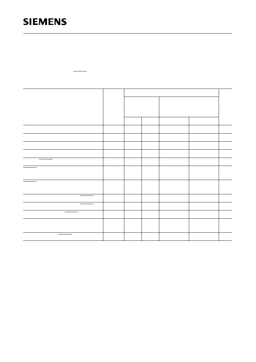
Semiconductor Group
70
1997-12-01
C505 / C505C
C505A / C505CA
AC Characteristics (16 MHz, 0.4 to 0.6 Duty Cycle)
V
CC
= 5 V +10%, ≠ 15%;
V
SS
= 0 V
T
A
= 0 to 70
∞
C for the SAB- versions
T
A
= 40 to 85
∞
C for the SAF- versions
(
C
L
for port 0, ALE and PSEN outputs = 100 pF;
C
L
for all other outputs = 80 pF)
Program Memory Characteristics
*)
Interfacing the C505 to devices with float times up to 20 ns is permissible. This limited bus contention will not
cause any damage to port 0 drivers.
Parameter
Symbol
Limit Values
Unit
16-MHz clock
Duty Cycle
0.4 to 0.6
Variable Clock
1/CLP= 2 MHz to 16 MHz
min.
max.
min.
max.
ALE pulse width
t
LHLL
48
≠
CLP - 15
≠
ns
Address setup to ALE
t
AVLL
10
≠
TCL
Hmin
-15
≠
ns
Address hold after ALE
t
LLAX
10
≠
TCL
Hmin
-15
≠
ns
ALE to valid instruction in
t
LLIV
≠
75
≠
2 CLP - 50
ns
ALE to PSEN
t
LLPL
10
≠
TCL
Lmin
-15
≠
ns
PSEN pulse width
t
PLPH
73
≠
CLP+
TCL
Hmin
-15
≠
ns
PSEN to valid instruction in
t
PLIV
≠
38
≠
CLP+
TCL
Hmin
- 50
ns
Input instruction hold after PSEN
t
PXIX
0
≠
0
≠
ns
Input instruction float after PSEN
t
PXIZ
*)
≠
15
≠
TCL
Lmin
-10
ns
Address valid after PSEN
t
PXAV
*)
20
≠
TCL
Lmin
- 5
≠
ns
Address to valid instruction in
t
AVIV
≠
95
≠
2 CLP +
TCL
Hmin
-55
ns
Address float to PSEN
t
AZPL
-5
≠
-5
≠
ns
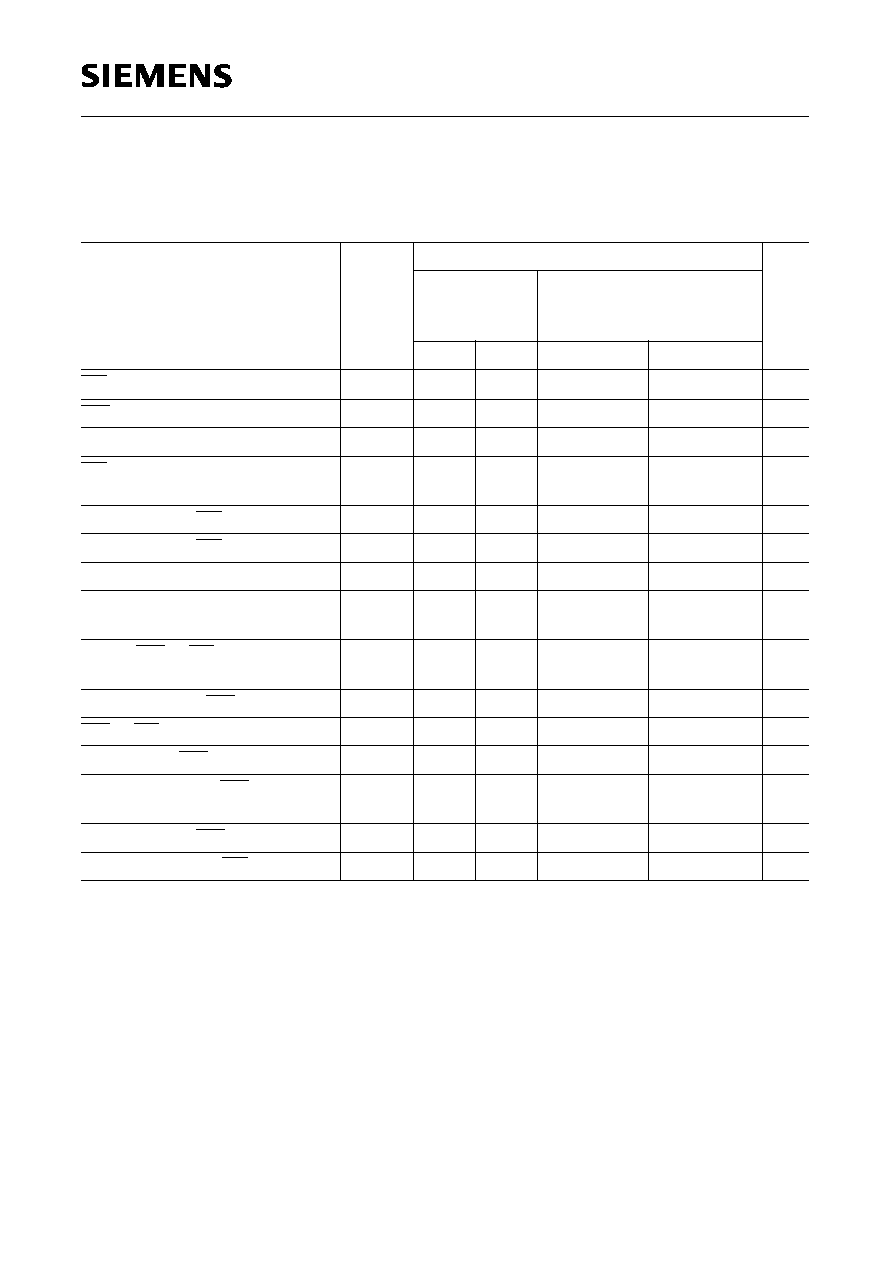
Semiconductor Group
71
1997-12-01
C505 / C505C
C505A / C505CA
AC Characteristics (16 MHz, 0.4 to 0.6 Duty Cycle, cont'd)
External Data Memory Characteristics
Parameter
Symbol
Limit Values
Unit
16-MHz clock
Duty Cycle
0.4 to 0.6
Variable Clock
1/CLP= 2 MHz to 16 MHz
min.
max.
min.
max.
RD pulse width
t
RLRH
158
≠
3 CLP - 30
≠
ns
WR pulse width
t
WLWH
158
≠
3 CLP - 30
≠
ns
Address hold after ALE
t
LLAX2
48
≠
CLP - 15
≠
ns
RD to valid data in
t
RLDV
≠
100
≠
2 CLP+
TCL
Hmin
- 50
ns
Data hold after RD
t
RHDX
0
≠
0
≠
ns
Data float after RD
t
RHDZ
≠
51
≠
CLP - 12
ns
ALE to valid data in
t
LLDV
≠
200
≠
4 CLP - 50
ns
Address to valid data in
t
AVDV
≠
200
≠
4 CLP +
TCL
Hmin
-75
ns
ALE to WR or RD
t
LLWL
73
103
CLP +
TCL
Lmin
- 15
CLP+
TCL
Lmin
+ 15
ns
Address valid to WR
t
AVWL
95
≠
2 CLP - 30
≠
ns
WR or RD high to ALE high
t
WHLH
10
40
TCL
Hmin
- 15
TCL
Hmin
+ 15
ns
Data valid to WR transition
t
QVWX
5
≠
TCL
Lmin
- 20
≠
ns
Data setup before WR
t
QVWH
163
≠
3 CLP +
TCL
Lmin
- 50
≠
ns
Data hold after WR
t
WHQX
5
≠
TCL
Hmin
- 20
≠
ns
Address float after RD
t
RLAZ
≠
0
≠
0
ns
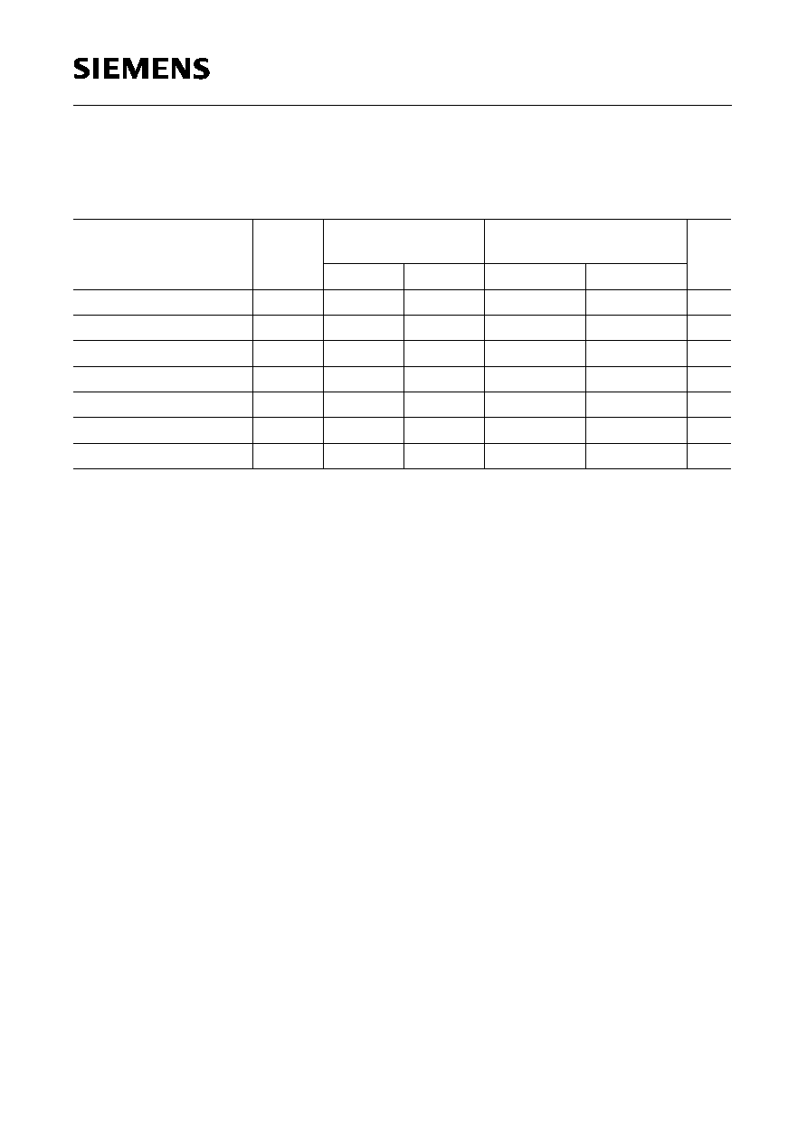
Semiconductor Group
72
1997-12-01
C505 / C505C
C505A / C505CA
AC Characteristics (16 MHz, 0.4 to 0.6 Duty Cycle, cont'd)
Note: The 16 MHz values in the tables are given as an example for a typical duty cycle variation
of the oscillator clock from 0.4 to 0.6.
External Clock Drive Characteristics
Parameter
Symbol
CPU Clock = 16 MHz
Duty Cycle 0.4 to 0.6
Variable CPU Clock
1/CLP = 2 to 16 MHz
Unit
min.
max.
min.
max.
Oscillator period
CLP
62.5
62.5
62.5
500
ns
High time
TCL
H
25
≠
25
CLP - TCL
L
ns
Low time
TCL
L
25
≠
25
CLP - TCL
H
ns
Rise time
t
R
≠
10
≠
10
ns
Fall time
t
F
≠
10
≠
10
ns
Oscillator duty cycle
DC
0.4
0.6
25 / CLP
1 - 25 / CLP
≠
Clock cycle
TCL
25
37.5
CLP * DC
min
CLP * DC
max
ns
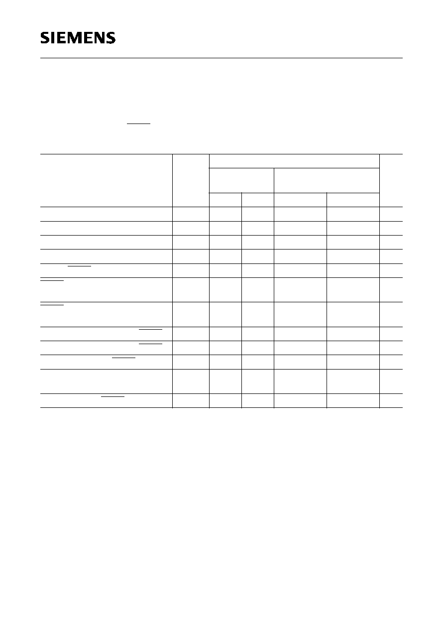
Semiconductor Group
73
1997-12-01
C505 / C505C
C505A / C505CA
AC Characteristics (20 MHz, 0.5 Duty Cycle)
V
CC
= 5 V + 10%, ≠ 15%;
V
SS
= 0 V
T
A
= 0 to 70
∞
C for the SAB- versions
T
A
= ≠ 40 to 85
∞
C for the SAF- versions
(
C
L
for port 0, ALE and PSEN outputs = 100 pF;
C
L
for all other outputs = 80 pF)
Program Memory Characteristics
*)
Interfacing the C505 to devices with float times up to 20 ns is permissible. This limited bus contention will not
cause any damage to port 0 drivers.
Parameter
Symbol
Limit Values
Unit
20 MHz clock
0.5 Duty Cycle
Variable Clock
1/CLP = 2 MHz to 20 MHz
min.
max.
min.
max.
ALE pulse width
t
LHLL
35
≠
CLP - 15
≠
ns
Address setup to ALE
t
AVLL
10
≠
CLP/2 - 15
≠
ns
Address hold after ALE
t
LLAX
10
≠
CLP/2 - 15
≠
ns
ALE to valid instruction in
t
LLIV
≠
55
≠
2 CLP - 45
ns
ALE to PSEN
t
LLPL
10
≠
CLP/2 - 15
≠
ns
PSEN pulse width
t
PLPH
60
≠
3/2 CLP
- 15
≠
ns
PSEN to valid instruction in
t
PLIV
≠
25
≠
3/2 CLP
- 50
ns
Input instruction hold after PSEN
t
PXIX
0
≠
0
≠
ns
Input instruction float after PSEN
t
PXIZ
*)
≠
20
≠
CLP/2 - 5
ns
Address valid after PSEN
t
PXAV
*)
20
≠
CLP/2 - 5
≠
ns
Address to valid instruction in
t
AVIV
≠
65
≠
5/2 CLP
- 60
ns
Address float to PSEN
t
AZPL
- 5
≠
- 5
≠
ns

Semiconductor Group
74
1997-12-01
C505 / C505C
C505A / C505CA
AC Characteristics (20 MHz, 0.5 Duty Cycle, cont'd)
External Data Memory Characteristics
Parameter
Symbol
Limit Values
Unit
20 MHz clock
0.5 Duty Cycle
Variable Clock
1/CLP = 2 MHz to 20 MHz
min.
max.
min.
max.
RD pulse width
t
RLRH
120
≠
3 CLP - 30
≠
ns
WR pulse width
t
WLWH
120
≠
3 CLP - 30
≠
ns
Address hold after ALE
t
LLAX2
35
≠
CLP - 15
≠
ns
RD to valid data in
t
RLDV
≠
75
≠
5/2 CLP- 50
ns
Data hold after RD
t
RHDX
0
≠
0
≠
ns
Data float after RD
t
RHDZ
≠
38
≠
CLP - 12
ns
ALE to valid data in
t
LLDV
≠
150
≠
4 CLP - 50
ns
Address to valid data in
t
AVDV
≠
150
≠
9/2 CLP - 75
ns
ALE to WR or RD
t
LLWL
60
90
3/2 CLP - 15
3/2 CLP + 15 ns
Address valid to WR
t
AVWL
70
≠
2 CLP - 30
≠
ns
WR or RD high to ALE high
t
WHLH
10
40
CLP/2 - 15
CLP/2 + 15
ns
Data valid to WR transition
t
QVWX
5
≠
CLP/2 - 20
≠
ns
Data setup before WR
t
QVWH
125
≠
7/2 CLP - 50
≠
ns
Data hold after WR
t
WHQX
5
≠
CLP/2 - 20
≠
ns
Address float after RD
t
RLAZ
≠
0
≠
0
ns
External Clock Drive Characteristics
Parameter
Symbol
Limit Values
Unit
Variable Clock
Freq. = 2 MHz to 20 MHz
min.
max.
Oscillator period
CLP
50
500
ns
High time
TCL
H
15
CLP-TCL
L
ns
Low time
TCL
L
15
CLP-TCL
H
ns
Rise time
t
R
≠
10
ns
Fall time
t
F
≠
10
ns
Oscillator duty cycle
DC
0.5
0.5
≠
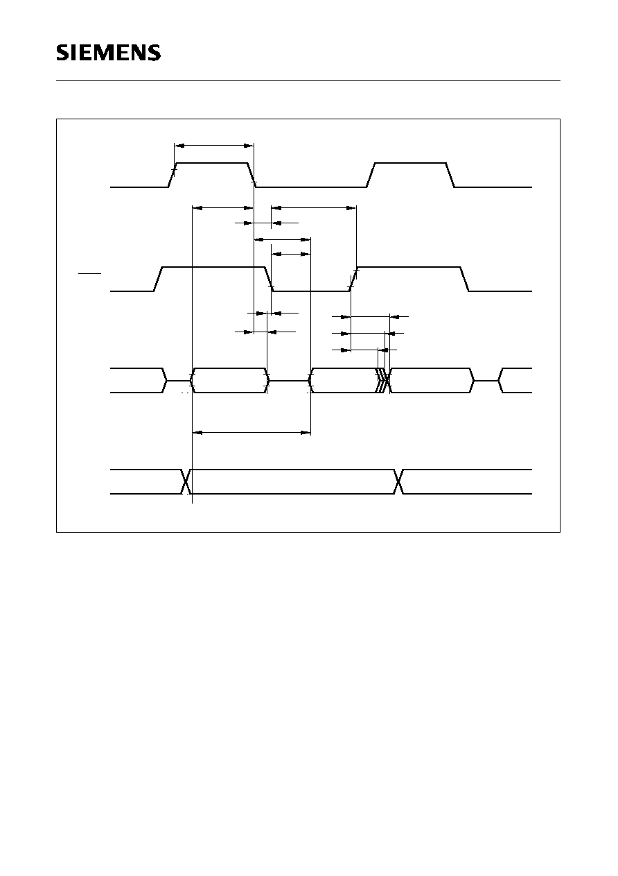
Semiconductor Group
75
1997-12-01
C505 / C505C
C505A / C505CA
Figure 31
Program Memory Read Cycle
MCT00096
ALE
PSEN
Port 2
LHLL
t
A8 - A15
A8 - A15
A0 - A7
Instr.IN
A0 - A7
Port 0
t
AVLL
PLPH
t
t
LLPL
t
LLIV
t
PLIV
t
AZPL
t
LLAX
t
PXIZ
t
PXIX
t
AVIV
t
PXAV
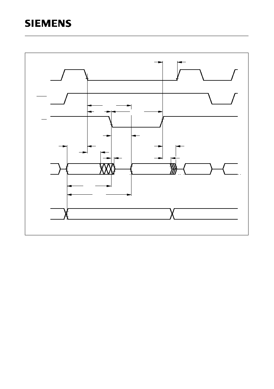
Semiconductor Group
76
1997-12-01
C505 / C505C
C505A / C505CA
Figure 32
Data Memory Read Cycle
MCT00097
ALE
PSEN
Port 2
WHLH
t
Port 0
RD
t
LLDV
t
RLRH
t
LLWL
t
RLDV
t
AVLL
t
LLAX2
t
RLAZ
t
AVWL
t
AVDV
t
RHDX
t
RHDZ
A0 - A7 from
Ri or DPL
from PCL
A0 - A7
Instr.
IN
Data IN
A8 - A15 from PCH
P2.0 - P2.7 or A8 - A15 from DPH
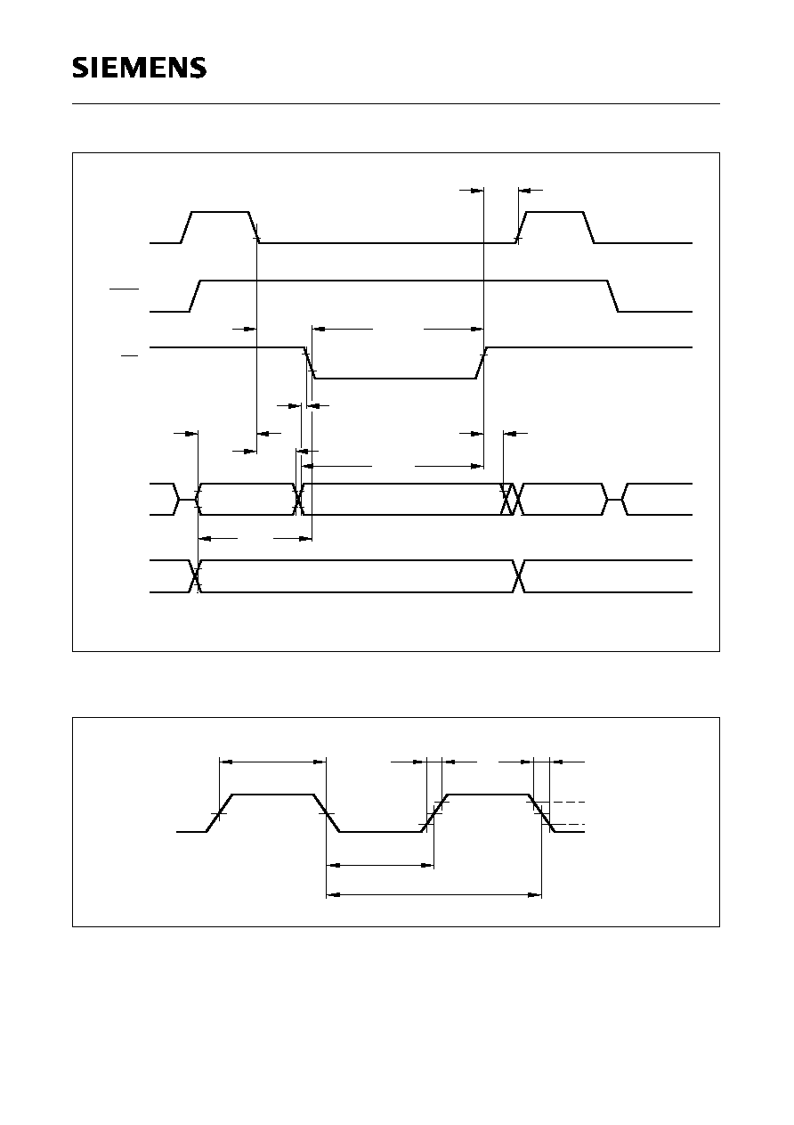
Semiconductor Group
77
1997-12-01
C505 / C505C
C505A / C505CA
Figure 33
Data Memory Write Cycle
Figure 34
External Clock Drive on XTAL1
MCT00098
ALE
PSEN
Port 2
WHLH
t
Port 0
WR
t
WLWH
t
LLWL
t
QVWX
t
AVLL
t
LLAX2
t
QVWH
t
AVWL
t
WHQX
A0 - A7 from
Ri or DPL
from PCL
A0 - A7
Instr.IN
Data OUT
A8 - A15 from PCH
P2.0 - P2.7 or A8 - A15 from DPH
TCL
H
TCL
L
CLP
t
R
t
F
0.2 V
CC
0.7
CC
V
- 0.1
MCT03310
XTAL1
Semiconductor Group
78
1997-12-01
C505 / C505C
C505A / C505CA
AC Characteristics of Programming Mode (C505A and C505CA only)
V
CC
= 5 V
±
10 %;
V
PP
= 11.5 V
±
5 %;
T
A
= 25
∞
C
±
10
∞
C
Parameter
Symbol
Limit Values
Unit
min.
max.
ALE pulse width
t
PAW
35
≠
ns
PMSEL setup to ALE rising edge
t
PMS
10
≠
Address setup to ALE, PROG, or PRD falling
edge
t
PAS
10
≠
ns
Address hold after ALE, PROG, or PRD
falling edge
t
PAH
10
≠
ns
Address, data setup to PROG or PRD
t
PCS
100
≠
ns
Address, data hold after PROG or PRD
t
PCH
0
≠
ns
PMSEL setup to PROG or PRD
t
PMS
10
≠
ns
PMSEL hold after PROG or PRD
t
PMH
10
≠
ns
PROG pulse width
t
PWW
100
≠
µ
s
PRD pulse width
t
PRW
100
≠
ns
Address to valid data out
t
PAD
≠
75
ns
PRD to valid data out
t
PRD
≠
20
ns
Data hold after PRD
t
PDH
0
≠
ns
Data float after PRD
t
PDF
≠
20
ns
PROG high between two consecutive PROG
low pulses
t
PWH1
1
≠
µ
s
PRD high between two consecutive PRD low
pulses
t
PWH2
100
ns
XTAL clock period
t
CLKP
83.3
500
ns
Semiconductor Group
79
1997-12-01
C505 / C505C
C505A / C505CA
Figure 35
Programming Code Byte - Write Cycle Timing
t
PAW
t
PMS
PAH
t
PAS
t
A8-A14
A0-A7
D0-D7
PCS
t
PWW
t
PCH
t
t
PWH
MCT03642
H, H
PALE
PMSEL1,0
Port 2
Port 0
PROG
Notes: PRD must be high during a programming write cycle.
Semiconductor Group
80
1997-12-01
C505 / C505C
C505A / C505CA
Figure 36
Verify Code Byte - Read Cycle Timing
t
PAW
t
PMS
PAH
t
PAS
t
A8-A14
A0-A7
PAD
t
D0-D7
t
PDH
t
PDF
PRD
t
PCS
t
PRW
t
PCH
t
t
PWH
MCT03643
H, H
PALE
PMSEL1,0
Port 2
Port 0
PRD
PROG must be high during a programming read cycle.
Notes:
Semiconductor Group
81
1997-12-01
C505 / C505C
C505A / C505CA
Figure 37
Lock Bit Access Timing
Figure 38
Version Byte Read Timing
H, L
H, L
D0, D1
D0, D1
t
PCS
PMS
t
PMH
t
t
PCH
PWW
t
PMS
t
PRD
t
t
PDH
PDF
t
PMH
t
PRW
t
MCT03644
PMSEL1,0
Port 0
PROG
PRD
PALE should be low during a lock bit read / write cycle.
Note:
e. g. FD
D0-7
t
PCS
PMS
t
t
PDH
PDF
t
PMH
t
MCT03645
Port 2
Port 0
PRD
PMSEL1,0
L, H
H
PRW
t
PRD
t
PCH
t
PROG must be high during a programming read cycle.
Note:
Semiconductor Group
82
1997-12-01
C505 / C505C
C505A / C505CA
ROM/OTP Verification Characteristics for C505
ROM Verification Mode 1 (C505-2R and C505C-2R only)
Figure 39
ROM Verification Mode 1
Parameter
Symbol
Limit Values
Unit
min.
max.
Address to valid data
t
AVQV
≠
5 CLP
ns
P1.0 - P1.7
P2.0 - P2.6
Port 0
Address
Data OUT
Address: P1.0 - P1.7 = A0 - A7
P2.0 - P2.5 = A8 - A14
Data:
P0.0 - P0.7 = D0 - D7
Inputs: P2.6, P2.7, PSEN =
ALE, EA =
RESET =
V
SS
V
IH
V
IH2
AVQV
t
MCT03693
Semiconductor Group
83
1997-12-01
C505 / C505C
C505A / C505CA
ROM/OTP Verification Characteristics for C505 (cont'd)
ROM/OTP Verification Mode 2
Figure 40
ROM/OTP Verification Mode 2
Parameter
Symbol
Limit Values
Unit
min.
typ
max.
ALE pulse width
t
AWD
≠
CLP
≠
ns
ALE period
t
ACY
≠
6 CLP
≠
ns
Data valid after ALE
t
DVA
≠
≠
2 CLP
ns
Data stable after ALE
t
DSA
4 CLP
≠
≠
ns
P3.5 setup to ALE low
t
AS
≠
t
CL
≠
ns
Oscillator frequency
1/ CLP
4
≠
6
MHz
MCT02613
t
ACY
t
AWD
t
DSA
DVA
t
t
AS
Data Valid
ALE
Port 0
P3.5

Semiconductor Group
84
1997-12-01
C505 / C505C
C505A / C505CA
Figure 41
AC Testing: Input, Output Waveforms
Figure 42
AC Testing : Float Waveforms
Figure 43
Recommended Oscillator Circuits for Crystal Oscillator
AC Inputs during testing are driven at
V
CC
- 0.5 V for a logic '1' and 0.45 V for a logic '0'.
Timing measurements are made at
V
IHmin
for a logic '1' and
V
ILmax
for a logic '0'.
0.45 V
V
CC
0.2
-0.1
+0.9
0.2
CC
V
Test Points
MCT00039
V
CC
-0.5 V
For timing purposes a port pin is no longer floating when a 100 mV change from load voltage
occurs and begins to float when a 100 mV change from the loaded
V
OH
/
V
OL
level occurs.
I
OL
/
I
OH
±
20 mA
MCT00038
V
Load
V
Load
-0.1 V
+0.1 V
Load
V
Timing Reference
Points
V
OH
-0.1 V
+0.1 V
OL
V
MCS03311
C
2 - 20
MHz
XTAL2
XTAL1
XTAL1
XTAL2
N.C.
External Oscillator
Signal
Crystal Oscillator Mode
Driving from External Source
Crystal Mode: C = 20 pF 10 pF (incl. stray capacitance)
C

Semiconductor Group
85
1997-12-01
C505 / C505C
C505A / C505CA
Figure 44
P-MQFP-44 Package Outline
GPM05622
P-MQFP-44-1 (SMD)
(Plastic Metric Quad Flat Package)
Sorts of Packing
Package outlines for tubes, trays etc. are contained in our
Data Book "Package Information"
Dimensions in mm
SMD = Surface Mounted Device