
Semiconductor Group
1
Type
Ordering Code
Package
SDA 3302-5
Q67000-H5112
P-DIP-18-5
SDA 3302-5X
Q67000-H5111
P-DSO-20-1 (SMD)
SDA 3302-5X6
Q67000-H5110
P-DSO-16-1 (SMD)
SDA 3302-5X
Q67006-H5111
P-DSO-20-1 Tape & Reel (SMD)
SDA 3302-5X6
Q67006-H5110
P-DSO-16-1 Tape & Reel (SMD)
02.97
GHz PLL with
I
2
C Bus
and Four Chip Addresses
SDA 3302 Family
Bipolar IC
Preliminary Data
Features
q
1-chip system for MPU
control
(I
2
C bus)
q
4 programmable chip addresses
q
Short pull-in time for quick channel
switch-over and optimized loop
stability
q
Charge pump output with switch
off option
q
Up to 3*) high current band switch
outputs (20 mA)
q
Up to 4*) output ports (5 mA)
*) depending on version
P-DIP-18-5
P-DSO-20-1
P-DSO-16-1

Semiconductor Group
2
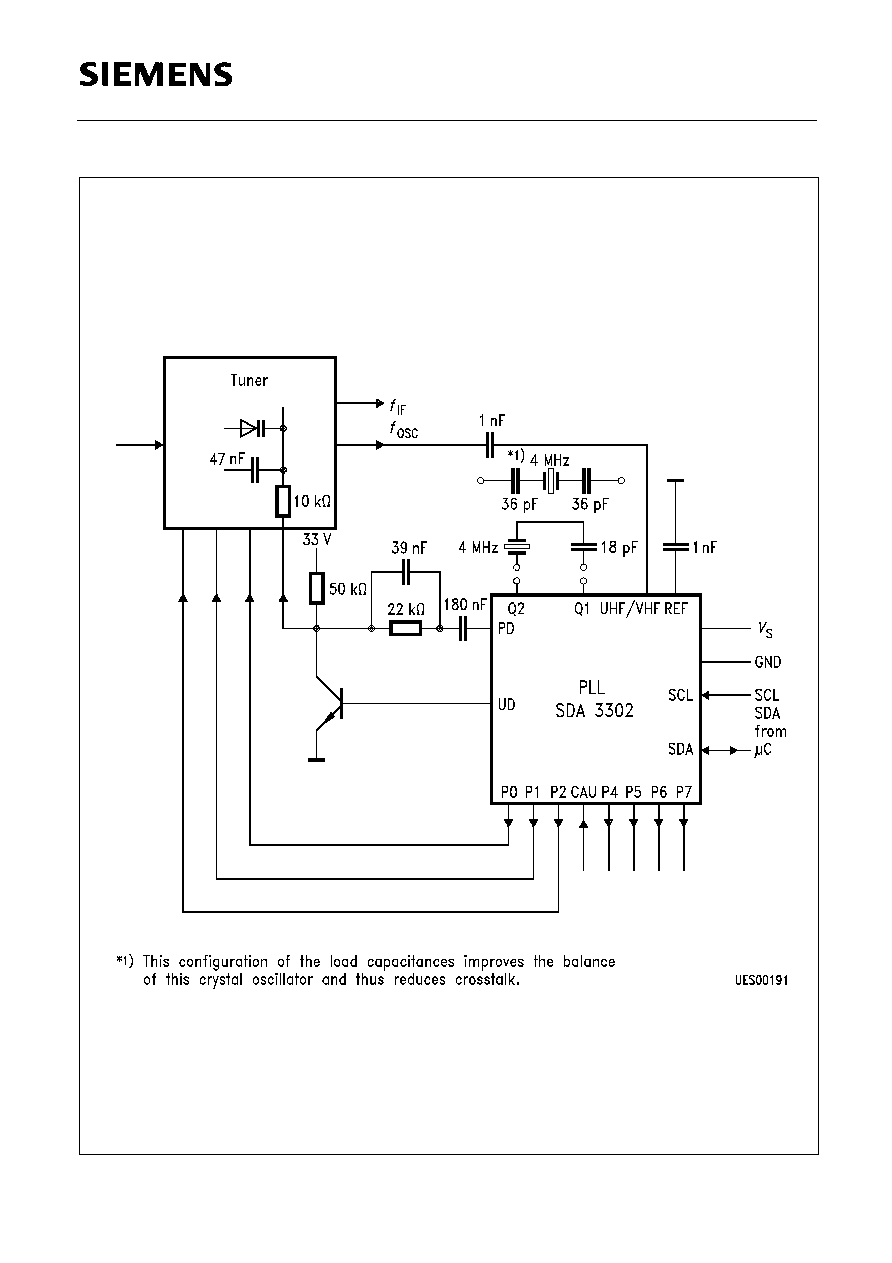
Functional Description
Combined with a VCO (tuner) the SDA 3302 device, with four hardware-switched chip
addresses, forms a digitally programmable phase-locked loop for use in television sets with
PLL frequency-synthesis tuning.
The PLL permits precise crystal-controlled setting of the frequency of the tuner oscillators
between 16 and 1300 MHz in increments of 62.5 kHz. The tuning process is controlled by a
microprocessor via an
I
2
C bus. The crystal oscillator generates a sinusoidal signal suppressing
the higher-order harmonics, which reduces the moir� noise considerably.
Circuit Description
Tuning Section (refer to block diagram)
UHF/VHF
The tuner signal is capacitively coupled at the UHF/VHF input and
subsequently amplified. The reference input REF should be decoupled to
ground using a capacitor of low series inductance. The signal passes
through an asynchronous divider with a fixed ratio of
P
= 8, an adjustable
divider with ratio
N
= 256 through 32767 and is then compared in a digital
phase/frequency detector to a reference frequency
f
REF
of 7.8125 kHz. The
latter is derived from a balanced, low-impedance 4 MHz crystal oscillator
Q1, Q2
(pin Q1, Q2), whose output signal is divided by
Q
= 512.
The phase detector has two outputs UP and DOWN that drive the two current
sources
I
+ and
I
� of a charge pump. If the negative edge of the divided VCO
signal appears prior to the negative edge of the reference signal, the
I
+
current source pulses for the duration of the phase difference. In the reverse
case the
I
� current source pulses.
PD, UD
When the two signals are in phase, the charge-pump output (PD) goes high-
impedance (PLL is locked). An active low-pass filter integrates the current
pulses to generate the tuning voltage for the VCO (internal amplifier an
external transistor at the UD output and an external RC circuitry). The
charge-pump output can also be set to high-impedance state when control
bit T0 = 1. Here it should be noted, however, that the tuning voltage can alter
over a long period in the high-impedance state as a result of self-discharge
in the peripheral circuitry. UD can be disconnected internally by the control
bit OS to enable external adjustments.
By means of a control bit 5I the pump current can be switched between two
values by software. This switchover permits alteration of the control
response of the PLL in the locked-in state. In this way different VCO gains in
the different TV bands can be compensated for example.
REF
SDA 3302 Family

Semiconductor Group
3
Circuit Description (cont'd)
P0-P2
The software-switched outputs (P0, P1, P2) can be used for direct band
selection (20-mA current output).
P4-P7
P4, P5, P6 and P7 are open-collector outputs for a variety of different
purposes. The test bit T1 = 1 switches the test signals
f
REF
(4 MHz/512) and
Cy (divided input signal) to P6 and P7.
CAS
Four different chip addresses can be set by appropriate connection of pin
CAS.
I
2
C-Bus Interface
SCL, SDA
Data are exchanged between the processor and the PLL on the
I
2
C bus. The
clock is produced by the processor (input SCL), while pin SDA works as an
input or output depending on the direction of the data (open collector;
external pullup resistor). Both inputs have hysteresis and a lowpass
characteristic, which enhances the noise immunity of the
I
2
C bus.
The data from the processor are applied to an
I
2
C bus controller and filed in
registers according to their function. When the bus is free, both lines are in
the marking state (SDA, SCL are high). Each telegram begins with a start
condition and ends with the stop condition. Start condition: SDA goes low
while SCL remains high; stop condition: SDA goes high while SCL remains
high. All further data exchanges occur while SCL is low and are accepted by
the controller with the positive clock edge.
For what follows, refer to the table of logic allocations.
All telegrams are transmitted byte by byte, followed by a ninth clock pulse,
during which the controller puts the SDA line on low (acknowledge condition).
The first byte consists of seven address bits, with which the processor
selects the PLL from a number of peripheral devices (chip select). The eighth
bit is always low. In the data portion of the telegram the first bit of the first or
third data byte determines whether a divider ratio or control information
follows. In each case the byte following the first byte must be of the same
data type (or a stop condition).
V
S
, GND
When the supply voltage is applied, a power-on reset circuit prevents the PLL
from putting the SDA line on low, which would block the bus.
SDA 3302 Family

Semiconductor Group
4
Circuit Description (cont'd)
Logic Allocations
Divider Ratio
N
= 16384
�
n14 + 8192
�
n13 + 4096
�
n12 + 2048
�
n11 + 1024
�
n10 + 512
�
n9 + 256
�
n8 +
+ 128
�
n7 + 64
�
n6 + 32
�
n5 + 16
�
n4 + 8
�
n3 + 4
�
n2 + 2
�
n1
+ n0
Band Selection
P2-P0 = 1
Open-collector output is active.
Port Outputs
P7-P4 = 1
Open-collector output is active.
Pump Current Switchover
5I = 1
High current.
UD Disable
OS = 1
V
D
is disabled.
Test Mode
T1, T0 = 0,0
Normal mode
T1 = 1
P6 =
f
REF
; P7 = Cy
T0 = 1
Tristate charge pump PD is in high-impedance.
MSB
A = Acknowledge
Address byte
1
1
0
0
0
MA1
MA0
0
A
Prog. divider byte 1
0
n14
n13
n12
n11
n10
n9
n8
A
Prog. divider byte 2
n7
n6
n5
n4
n3
n2
n1
n0
A
Control info. byte 1
1
5I
T1
T0
1
1
1
OS
A
Control info. byte 2
P7
P6
P5
P4
X
P2
P1
P0
A
SDA 3302 Family

Semiconductor Group
5
Circuit Description (cont'd)
Chip-Address Switching
Pulse Diagram
Telegram Examples
Start-Addr-DR1-DR2-CW1-CW2-Stop
Start
= start condition
Start-Addr-CW1-CW2-DR1-DR2-Stop
Addr
= address
Start-Addr-DR1-DR2-CW1-Stop
DR1
= divider ratio 1st byte
Start-Addr-CW1-CW2-DR1-Stop
DR2
= divider ratio 2nd byte
Start-Addr-DR1-DR2-Stop
CW1
= control word 1st byte
Start-Addr-CW1-CW2-Stop
CW2
= control word 2nd byte
Start-Addr-DR1-Stop
Stop
= stop condition
MA1
MA0
Voltage on CAS
0
0
(0-0.1)
V
S
0
1
open
1
0
(0.4-0.6)
V
S
1
1
(0.9-1)
V
S
SDA 3302 Family

Semiconductor Group
6
Pin Configuration (SDA 3302-5)
(top view)
P-DIP-18-5
SDA 3302 Family

Semiconductor Group
7
Pin Definitions and Functions (SDA 3302-5)
Pin No.
Symbol
Function
1
PD
Active-filter input/charge-pump output
2
Q1
Crystal
3
Q2
Crystal
4
SDA
Data input/output for
I
2
C bus
5
SCL
Clock input for
I
2
C bus
6
P7
Port output (open collector)
7
P6
Port output (open collector)
8
P5
Port output (open collector)
9
P4
Port output (open collector)
10
CAS
Chip-address switchover
11
P2
Port output (open collector)
12
P1
Port output (open collector)
13
P0
Port output (open collector)
14
V
S
Supply voltage
15
UHF/VHF
Signal input
16
REF
Amplifier reference input
17
GND
Ground
18
UD
Output active filter
SDA 3302 Family
Semiconductor Group
8
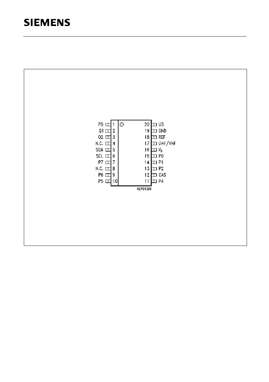
Pin Configuration (SDA 3302-5X)
(top view)
P-DSO-20-1
SDA 3302 Family

Semiconductor Group
9
Pin Definitions and Functions (SDA 3302-5X)
Pin No.
Symbol
Function
1
PD
Active-filter input/charge-pump output
2
Q1
Crystal
3
Q2
Crystal
4
N.C.
Not connected
5
SDA
Data input/output for
I
2
C bus
6
SCL
Clock input for
I
2
C bus
7
P7
Port output (open collector)
8
N.C.
Not connected
9
P6
Port output (open collector)
10
P5
Port output (open collector)
11
P4
Port output (open collector)
12
CAS
Chip-address switchover
13
P2
Port output (open collector)
14
P1
Port output (open collector)
15
P0
Port output (open collector)
16
V
S
Supply voltage
17
UHF/VHF
Signal input
18
REF
Amplifier reference input
19
GND
Ground
20
UD
Active-filter output
SDA 3302 Family

Semiconductor Group
10
Pin Configuration (SDA 3302-5X6)
(top view)
P-DSO-16-1
SDA 3302 Family

Semiconductor Group
11
Pin Definitions and Functions (SDA 3302-5X6)
Pin No.
Symbol
Function
1
PD
Active-filter input/output pump output
2
Q1
Crystal
3
Q2
Crystal
4
SDA
Data input/output for
I
2
C bus
5
SCL
Clock input for
I
2
C bus
6
P7
Port output (open collector)
7
P6
Port output (open collector)
8
P5
Port output (open collector)
9
P4
Port output (open collector)
10
CAS
Chip-address switchover
11
P1
Port output (open collector)
12
V
S
Supply voltage
13
UHF/VHF
Signal input
14
REF
Amplifier reference input
15
GND
Ground
16
UD
Output active filter
SDA 3302 Family

Semiconductor Group
12
Pin Definitions and Functions, Reference List
SDA 3302
P-DIP-18-5
Pin No.
SDA 3302X
P-DSO-20-1
Pin No.
SDA 3302X6
P-DSO-16-1
Pin No.
Symbol
Function
1
1
1
PD
Input active-filter input charge
pump output
2
2
2
Q1
Crystal
3
3
3
Q2
Crystal
-
4
-
N.C.
Not connected
4
5
4
SDA
Data input/output for
I
2
C bus
5
6
5
SCL
Clock input for
I
2
C bus
6
7
6
P7
Port output (open collector)
-
8
-
N.C.
Not connected
7
9
7
P6
Port output (open collector)
8
10
8
P5
Port output (open collector)
9
11
9
P4
Port output (open collector)
10
12
10
CAS
Chip-address switchover
11
13
-
P2
Port output (open collector)
12
14
11
P1
Port output (open collector)
13
15
-
P0
Port output (open collector)
14
16
12
V
S
Supply voltage
15
17
13
UHF/VHF
Signal input
16
18
14
REF
Amplifier reference input
17
19
15
GND
Ground
18
20
16
UD
Output active filter
SDA 3302 Family

Semiconductor Group
13
Block Diagram SDA 3302-5
Pin nos. refer to P-DIP-18 package only. For other packages, see reference list on page 16
SDA 3302 Family

Semiconductor Group
14
2) Pin nos. refer to P-DIP-18 package
Absolute Maximum Ratings
T
A
= 25
�
C
Parameter
Symbol
2)
Limit Values
Unit
Remarks
min.
max.
Supply voltage
V
S
� 0.3
6
V
Output PD
V
1
� 0.3
V
S
V
Crystal Q1
V
2
� 0.3
V
S
V
Crystal Q2
V
3
� 0.3
V
S
V
Bus input/output SDA
V
4
� 0.3
6
V
Bus input SCL
V
5
� 0.3
6
V
Port output P7, P6, P5, P4
V
6, 7, 8, 9
� 0.3
16
V
Chip-address switchover
V
10
� 0.3
V
S
V
Port output P2, P1, P0
V
11, 12, 13
� 0.3
16
V
open collector
Signal input UHF/VHF
V
15
� 0.3
0.3
V
for
V
S
= 0 V
Reference input REF
V
16
� 0.3
0.3
V
for
V
S
= 0 V
Output active filter UD
V
18
� 0.3
V
S
V
Bus output SDA
I
4L
� 1
5
mA
open collector
Port output P7, P6, P5, P4
I
6L, 7L, 8L, 9L
� 1
5
mA
open collector
Port output P2, P1, P0
I
11L, 12L, 13L
� 1
20
mA
open collector
Chip temperature
T
C
125
�
C
Total port output current
Z
IL
25
mA
Storage temperature
T
stg
� 40
125
�
C
Thermal resistance (system-air)
R
thSA
80
K/W
SDA 3302 Family

Semiconductor Group
15
Absolute Maximum Ratings
T
A
= 25
�
C
Parameter
Symbol
2)
Limit Values
Unit
Remarks
min.
max.
Operating Range
Supply voltage
V
S
4.5
5.5
V
Ambient temperature
T
A
� 20
80
�
C
Input frequency
f
15
16
1300
MHz
Crystal frequency
f
2, 3
4
MHz
Programmable divider factor
N
256
32767
1) Design note: no 100 % final inspection.
2) Pin nos. refer to P-DIP-18 package
SDA 3302 Family

Semiconductor Group
16
Characteristics
V
S
= 5 V;
T
A
= 25
�
C
Parameter
Symbol
2)
Limit Values
Unit
Test Condition
Test
Circuit
min.
typ.
max.
Current
consumption
I
S
35
mA
V
S
= 5 V
1
Crystal-oscillator
frequency
f
2, 3
3.99975 4.000 4.00025 MHz
series capaci-
tance 18 pF;
f
xtal
= 4 MHz
1
Oscillator level
1)
(Voltage across
crystal)
V
2, 3
2.6
Vpp
Margin from 1st
1)
and 2nd harmonic
20
dB
Input Sensitivity UHF/VHF
a
15
a
15
a
15
� 27/10
� 27/10
� 27/10
3/315
3/315
3/315
3)
f
15
= 70-500 MHz
f
15
= 1000 MHz
f
15
= 1100 MHz
2
2
2
Band-Select Outputs P0-P2 (switch with open collector)
Reserve current
I
13H
10
�
A
V
13H
= 13.5 V
3
Residual voltage
V
13L
0.5
V
I
13H
= 20 mA
3
Port Outputs P4-P7 (switch with open collector)
Reserve current
I
9H
10
�
A
V
9H
= 13.5 V
4
Residual voltage
V
9L
0.5
V
I
9L
= 1.7 mA
4
Note: The sum of the currents in ports P0-P7 must not exceed 25 mA
Phase-Detector Output PD
Pump current
I
1H
�
90
�
230
�
300
�
A
5
I
= HIGH;
V
1
= 2 V
Pump current
I
1H
�
22
�
50
�
75
�
A
5
I
= LOW;
V
1
= 2 V
Output voltage
V
1L
1.0
2.5
V
locked
1) Design note: no 100 % final inspection.
2) Pin nos. refer to P-DIP-18 package
3) dBm/mV
rms
into 50
SDA 3302 Family

Semiconductor Group
17
Output Active Filter UD (T0 = 1)
Output current
�
I
18
500
�
A
V
18
= 0.8 V;
I
IH
= 90
�
A
5
Output voltage
V
18
100
mV
V
1L
= 0 V
5
Output voltage
V
18
500
mV
OS = 1
5
Chip-Address Switchover
Input current
I
10H
50
�
A
V
10H
= 5 V
7
Input current
� I
10H
50
�
A
V
10H
= 0 V
7
Bus Inputs SCL, SDA
Input voltage
V
5H
V
5L
3
5.5
5.5
V
V
6
6
Input current
I
5H
10
�
A
V
5H
=
V
S
6
Input current
�
I
5L
20
�
A
V
5L
= 0 V
6
Output SDA (open collector)
Reverse current
I
4H
10
�
A
V
4H
= 5.5 V
6
Output voltage
V
4L
0.4
V
I
4L
= 3 mA
6
Edges SCL, SDA
Rise time
t
R
1
�
s
6
Fall time
t
F
0.3
�
s
6
Shift Clock SCL
Frequency
f
5
0
100
kHz
6
H-pulse width
t
5H
4
�
s
6
L-pulse width
t
5L
4.7
�
s
6
2) Pin nos. refer to P-DIP-18 package
Characteristics (cont'd)
V
S
= 5 V;
T
A
= 25
�
C
Parameter
Symbol
2)
Limit Values
Unit
Test Condition
Test
Circuit
min.
typ.
max.
SDA 3302 Family

Semiconductor Group
18
Start
Setup time
t
SUSta
4.7
�
s
6
Hold time
t
HDSta
4
�
s
6
Stop
Setup time
t
SUsto
4.7
�
s
6
Bus free
t
BUF
4.7
�
s
6
Data Exchange
Setup time
t
SUDat
0.25
�
s
6
Hold time
t
HDDat
0
�
s
6
Input hysteresis
1)
SCL, SDA
300
mV
Lowpass cutoff
1)
frequency
SCL, SDA
500
kHz
1) Design note: no 100 % final inspection.
2)
Pin nos. refer to P-DIP-18 package
Characteristics (cont'd)
V
S
= 5 V;
T
A
= 25
�
C
Parameter
Symbol
2)
Limit Values
Unit
Test Condition
Test
Circuit
min.
typ.
max.
SDA 3302 Family

Semiconductor Group
19
Test Circuit 1
SDA 3302 Family

Semiconductor Group
20
Test Circuit 2
Test Circuit 3
SDA 3302 Family

Semiconductor Group
21
Test Circuit 4
Test Circuit 5
SDA 3302 Family
Semiconductor Group
22
Test Circuit 6
Test Circuit 7
I
2
C Bus Timing Diagram
SDA 3302 Family
Semiconductor Group
23
Application Circuit
SDA 3302 Family

Semiconductor Group
24
Application Circuit
Calculation of Loop Filter
Loop bandwidth
R
=
(
I
p
�
K
VCO
) / (
C
1
�
P
�
N
)
Attenuation:
= 0.5
�
R
�
R
�
C
1
P
= prescaler
N
= programmable divider
I
p
= pump current
K
VCO
= tuner slope
R
,
C
1
= loop filter
Example for channel 47:
P
= 8,
N
= 11520,
I
p
= 100
�
A;
K
VCO
= 18.7 MHz/V,
R
= 22 k
,
C
1
= 180 nF,
R
= 336 Hz,
f
r
= 54 Hz,
= 0.67
Standard dimensioning:
C
2
=
C
1/5
Note: The high-impedance port outputs and CAS can be blocked against external noise with
a capacitor of 1 nF.
SDA 3302 Family

Semiconductor Group
25
Input Sensitivity
I
2
C Bus Noise Immunity
The sinusoidal noise pulses are applied via a coupling capacitance of 33 pF to SCL and SDA
inputs.
SDA 3302 Family

Semiconductor Group
26
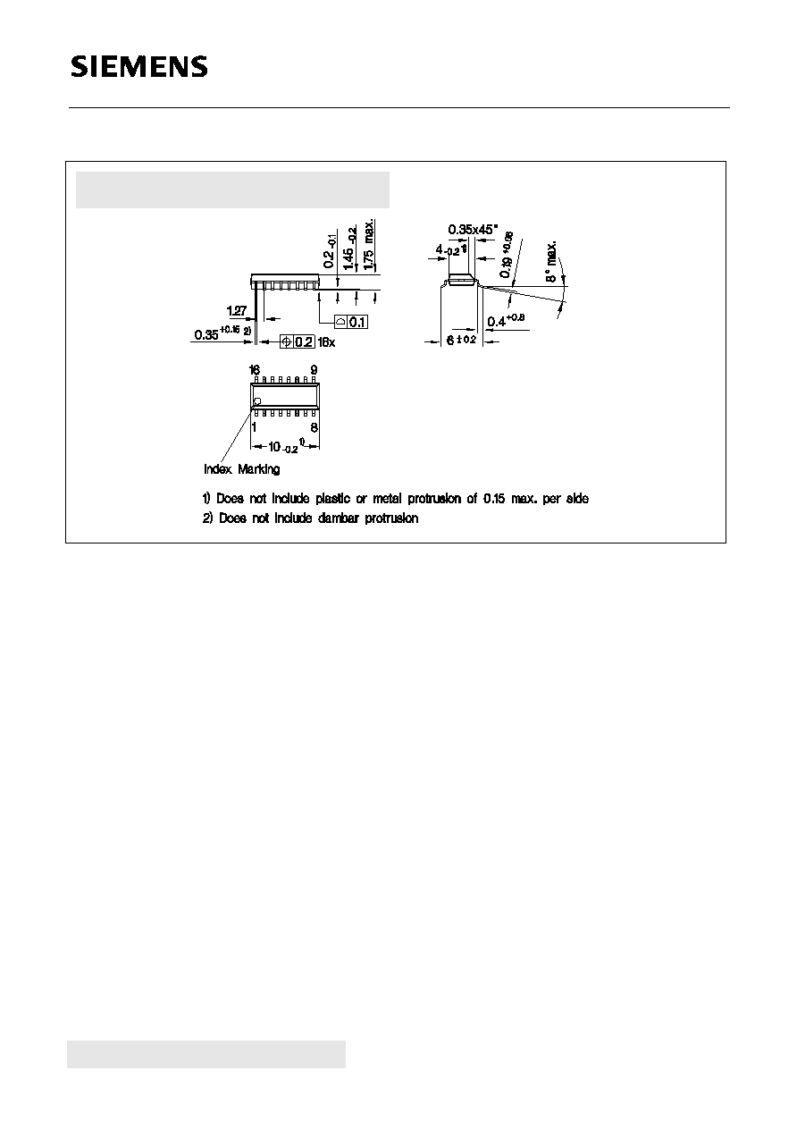
Package Outlines
Plastic-Package, P-DIP-18-5
(Plastic Dual In-Line Package)
GPD05586
Plastic-Package, P-DSO-20-1 (SMD)
(Plastic Dual Small Outline Package)
GPS05094
SDA 3302 Family
Semiconductor Group
27
SDA 3302 Family
Sorts of Packing
Package outlines for tubes, trays etc. are contained in our
Data Book "Package Information"
SMD = Surface Mounted Device
Dimensions in mm
Plastic-Package, P-DSO-16-1 (SMD)
(Plastic Dual Small Outline Package)
GPS051
19