
ICs for Consumer Electronics
SDA 525X to SDA 525X-2 V2.0
Delta Specification V2.0
1998-10-08
SDA 525X to SDA 525X-2
Revision History:
Current Version: 1998-10-08
Previous Version:
1998-03-10
Page
(in previous
Version)
Page
(in current
Version)
Subjects (major changes since last revision)
-
15
"VS sampling" inserted
-
17
"RGB and blanking skew" inserted
4, 5
4, 5
SDA 5254-57-2 with 10 pages optional
4, 5
4, 5
Also SDA 5253-2 available
14
14
Hardware compatibility, topics 5 to 8 added
18
21
Timing changed to 18 MHz
19
22
Changes in application circuit (Iref, CVBS, FIL3)
Edition 1998-10-08
Published by Siemens AG,
Bereich Halbleiter, Marketing-
Kommunikation, Balanstra�e 73,
81541 M�nchen
�
Siemens AG 1998.
All Rights Reserved.
Attention please!
As far as patents or other rights of third parties are concerned, liability is only assumed for components, not for
applications, processes and circuits implemented within components or assemblies.
The information describes the type of component and shall not be considered as assured characteristics.
Terms of delivery and rights to change design reserved.
For questions on technology, delivery and prices please contact the Semiconductor Group Offices in Germany or
the Siemens Companies and Representatives worldwide (see address list).
Due to technical requirements components may contain dangerous substances. For information on the types in
question please contact your nearest Siemens Office, Semiconductor Group.
Siemens AG is an approved CECC manufacturer.
Packing
Please use the recycling operators known to you. We can also help you � get in touch with your nearest sales
office. By agreement we will take packing material back, if it is sorted. You must bear the costs of transport.
For packing material that is returned to us unsorted or which we are not obliged to accept, we shall have to invoice
you for any costs incurred.
Components used in life-support devices or systems must be expressly authorized for such purpose!
Critical components
1
of the Semiconductor Group of Siemens AG, may only be used in life-support devices or
systems
2
with the express written approval of the Semiconductor Group of Siemens AG.
1 A critical component is a component used in a life-support device or system whose failure can reasonably be
expected to cause the failure of that life-support device or system, or to affect its safety or effectiveness of that
device or system.
2 Life support devices or systems are intended (a) to be implanted in the human body, or (b) to support and/or
maintain and sustain human life. If they fail, it is reasonable to assume that the health of the user may be endan-
gered.

SDA 525X-2
Table of Contents
Page
Semiconductor Group
3
1998-10-08
1
General Description . . . . . . . . . . . . . . . . . . . . . . . . . . . . . . . . . . . . . . . . .4
2
Complete Feature List Including New Features . . . . . . . . . . . . . . . . . . .4
3
Block Diagram . . . . . . . . . . . . . . . . . . . . . . . . . . . . . . . . . . . . . . . . . . . . . .6
4
Pin Configuration . . . . . . . . . . . . . . . . . . . . . . . . . . . . . . . . . . . . . . . . . . .7
4.1
P-MQFP-80-1, ROMless-Version (top view) . . . . . . . . . . . . . . . . . . . . . . . .7
4.2
P-LCC-84-2, Emulator-Version (top view) . . . . . . . . . . . . . . . . . . . . . . . . . .8
4.3
P-SDIP-52-1, ROM-Versions (top view) . . . . . . . . . . . . . . . . . . . . . . . . . . .9
4.4
P-MQFP-64-1, ROM-Versions (top view) . . . . . . . . . . . . . . . . . . . . . . . . .10
5
Pin Correspondence . . . . . . . . . . . . . . . . . . . . . . . . . . . . . . . . . . . . . . . .11
6
Differences of SDA 525x-2 Compared to SDA 525x . . . . . . . . . . . . . . .14
6.1
Hardware-Compatibility . . . . . . . . . . . . . . . . . . . . . . . . . . . . . . . . . . . . . . .14
6.2
Software-Compatibility . . . . . . . . . . . . . . . . . . . . . . . . . . . . . . . . . . . . . . . .14
6.3
Improved Performance Sync- and Data-Slicer . . . . . . . . . . . . . . . . . . . . .14
6.4
Crystal-locked Display-PLL . . . . . . . . . . . . . . . . . . . . . . . . . . . . . . . . . . . .14
6.5
Improved Interface to External RAM . . . . . . . . . . . . . . . . . . . . . . . . . . . . .14
6.6
No UART . . . . . . . . . . . . . . . . . . . . . . . . . . . . . . . . . . . . . . . . . . . . . . . . . .15
6.7
VS Sampling . . . . . . . . . . . . . . . . . . . . . . . . . . . . . . . . . . . . . . . . . . . . . . .15
6.8
RGB and Blanking Skew . . . . . . . . . . . . . . . . . . . . . . . . . . . . . . . . . . . . . .17
7
Registers of SDA 525x-2 . . . . . . . . . . . . . . . . . . . . . . . . . . . . . . . . . . . . .18
7.1
Address Space of SDA 525x-2 . . . . . . . . . . . . . . . . . . . . . . . . . . . . . . . . .20
8
Software Changes . . . . . . . . . . . . . . . . . . . . . . . . . . . . . . . . . . . . . . . . . .21
9
Timing . . . . . . . . . . . . . . . . . . . . . . . . . . . . . . . . . . . . . . . . . . . . . . . . . . . .21
10
Application Circuit . . . . . . . . . . . . . . . . . . . . . . . . . . . . . . . . . . . . . . . . . .22

SDA 525X-2
Semiconductor Group
4
1998-10-08
1
General Description
As its predecessors SDA 525x the SDA 525x-2 contains a slicer for VPS and TTX, an
accelerating acquisition hardware module, a display generator for "Level 1.5" TTX data,
and an 8 bit microcontroller running at 333 ns cycle time. The controller with dedicated
hardware guarantees flexibility, does most of the internal processing of TTX acquisition,
transfers data to/from the external memory interface and receives/transmits data via I
2
C
user interface. The block diagram shows the internal organization of the SDA 525x-2.
The slicer combined with dedicated hardware stores TTX data in a VBI buffer of
746 Byte. The microcontroller firmware performs all the acquisition tasks (hamming- and
parity-checks, page search and evaluation of header control bits) once per field.
This delta specification describes the differences of the SDA 525x-2 compared to the
SDA 525x as described in the preliminary data sheet 1997-09-01.
2
Complete Feature List Including
New Features
New features compared to SDA 525x-Specification, version 06/96 are printed in
italic
and bold
. As described in the errata sheet 03/97, release 1.0, the newer versions of the
SDA 525x and the SDA 525x-2 will
not have a serial port (UART)
any more.
� Acquisition:
� Feature selection via special function register
� Simultaneous reception of TTX, VPS, and WSS
� Fixed framing code for VPS and TTX
� Acquisition during VBI
� Direct access to VBI RAM buffer
� Acquisition of packets x/26, x/27, 8/30 (firmware)
� Assistance of all relevant checks (firmware)
� 1-bit framing code error tolerance (switchable)
� Display:
� Features selectable via special function register
� 50/60 Hz display
(optional 100 Hz)
� Level 1.5 serial attribute display pages
� Blanking and contrast reduction output
� 8 direct addressable display pages for SDA 5250-2, SDA 5254-2 to SDA 5257-2
(optional 10 pages)
� 1 direct addressable display page for SDA 5251-2 to SDA 5253-2
� 12
�
10 character matrix
� 96 character ROM (standard G0 character set)
�
156
national option characters for
12
languages (for European version)
� 288 characters for X/26 display
� 64 block mosaic graphic characters
� 32 characters for OSD in expanded character ROM + 32 characters
inside OSD box

SDA 525X-2
Semiconductor Group
5
1998-10-08
� Conceal/reveal
� Transparent foreground/background - inside/outside of a box
� Contrast reduction inside/outside of a box
� Cursor (color changes from foreground to background color)
� Flash (flash rate 1s,
not depending on field rate
)
� Programmable horizontal and vertical sync delay
� Full screen background color in outer screen
� Double size/double width/double height characters
� Synchronization:
� Display synchronization to sandcastle or Horizontal Sync (HS)
and Vertical Sync (VS)
� Microcontroller:
� 8 bit C500-CPU (8051 compatible)
� CPU-clock 18 MHz,
external 6-MHz-crystal
� 333 ns instruction cycle
� Parallel 8-bit data and 16 ... 19-bit address bus (ROMless-Version)
� Eight 16-bit data pointer registers (DPTR)
� Two 16-bit timers
� Watchdog timer
� Capture compare timer for infrared remote control decoding
� 256 bytes on-chip RAM
� 8 KByte on-chip display-RAM (access via MOVX) SDA 5250-2, SDA 5254-2 to
SDA 5257-2
(optional 10 Kbyte)
� 1 Kbyte on-chip display-RAM (access via MOVX) for SDA 5251-2 to SDA 5253-2
� 1 Kbyte on-chip ACQ-buffer-RAM (access via MOVX)
� 1 Kbyte on-chip extended-RAM (access via MOVX) for SDA 5250-2 and
SDA 5254-2 to SDA 5257-2
� 6 channel 8-bit pulse width modulation unit
� 2 channel 14-bit pulse width modulation unit
� 4 multiplexed ADC inputs with 8-bit resolution
� One 8-bit I/O port with open drain output and optional I
2
C-Bus emulation
� Two 8-bit multifunctional I/O ports
� One 4-bit port working as digital or analog inputs
� One 3-bit I/O port with optional RAM/ROM address expansion up to 512 Kbyte
(ROMless-Version)
� P-SDIP-52-1/P-MQFP-64-1 package for ROM-Versions (SDA 5251-2 to
SDA 5253-2, SDA 5254-2 to SDA 5257-2)
� P-MQFP-80-1 package for ROMless-Version (SDA 5250M-2)
� P-LCC-84-2 package for Emulator-Version (SDA 5250-2)
� 5 V supply voltage
SDA 525X-2
Semiconductor Group
6
1998-10-08
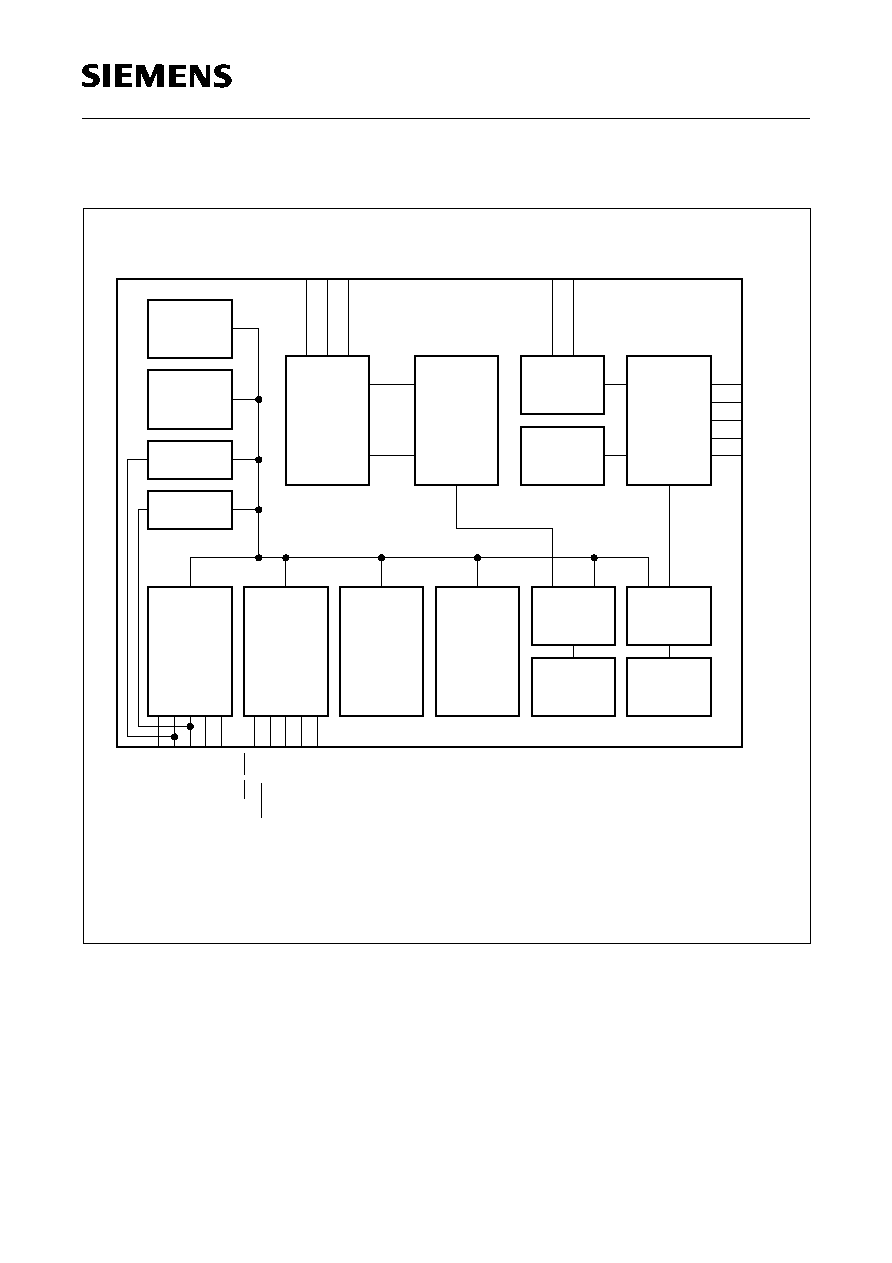
3
Block Diagram
Figure 1
Differences compared to SDA 525x according to preliminary specification 06/96:
1. UART is not supported.
2. RGB-outputs deliver a current instead of a voltage.
3. Instead of FIL1SLC/FIL2SLC/FIL3SLC only FIL3 is needed with changed external
device dimensions.
4. LCIN and LCOUT are not needed any more.
UES09854
C500
CPU
(8051-comp.)
incl.
Timer 0/1
256 Kbyte
Management
Unit
(MMU)
Memory
Extended
1 Kbyte
Data
RAM
ROM
Memory
Program
VBI Buffer
1 Kbyte
Dual Port
Interface
Interface
RAM
Display
Dual Port
Display
Generator
Display
ROM
448*12*10
Timing
Character
Acquisition
PWM
ADC
Watchdog
Timer
Capture
Timer
Compare
TTX, VPS
Slicer
TTC
TTD
R
B
COR
G
BLAN
CVBS
FIL3
I
VS
HS/SC
P3
P1
XTAL1, XTAL2
P2
P0
A(16:0)
PSEN, ALE
RD, WR
D(7:0)
P4.1(A18), P4.0(A17)
2)
3)
4)
1)
Only ROM-versions
Only ROMless-version
2)
Only SDA 5250-2 and
3)
8 K (opt. 10 K) byte for SDA 5250-2
4)
8 K for SDA 5254-2 to SDA 5257-2
1 Kbyte for SDA 5251-2 and SDA 5252-2
SDA 5254-2 to SDA 5257-2
1)
REF
SDA 525X-2
Semiconductor Group
7
1998-10-08
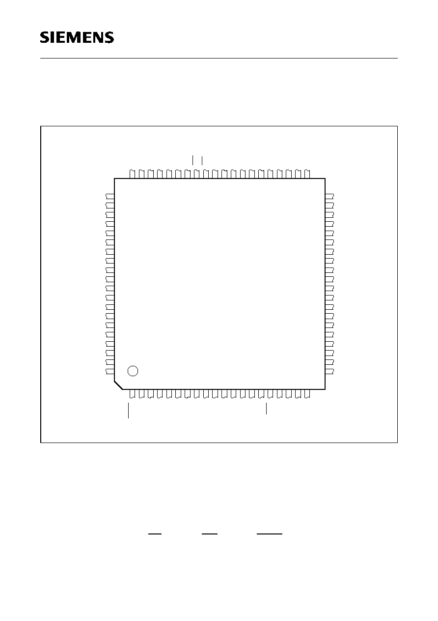
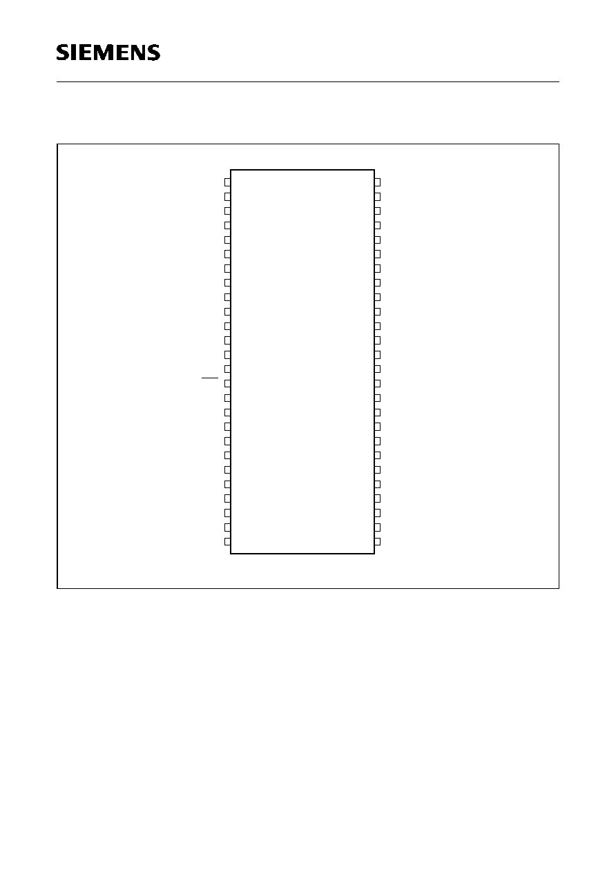
4
Pin Configuration
4.1
P-MQFP-80-1, ROMless-Version (top view)
Figure 2
Differences compared to SDA 525x according to preliminary specification 06/96:
1. RGB-outputs deliver a current instead of a voltage (Pins 45, 46, 47).
2. Instead of FIL1SLC/FIL2SLC/FIL3SLC only FIL3 is needed with changed external
device dimensions (Pin 69). Former FIL1SLC and FIL2SLC remain "not connected"
(Pins 70, 71).
3. LCIN and LCOUT are not needed any more and are now used for RD and WR (see 4.)
4. P-MQFP-80-1 now has RD (Pin 52), WR (53) and PSEN (1) Pins to connect external
RAM.
`n.c.' = `not connected' means: Pins must be left open.
UEP09855
73
P3.4
P3.3
P3.2
CVBS
P3.7
P3.6
P3.5
P1.5
P3.1
P1.7
P3.0
P1.6
2
78
80
79
1
77
76
75
74
3 4 5
P1.2
P1.4
P1.3
P1.0
P1.1
9
6 7 8
11
10
12
P2.3
FIL3
N.C.
N.C.
P2.2
P2.1
P2.0
P0.6
P0.7
64
69
71
72
70
68
67
66
65
P0.3
59
60
62
63
61
58 57 56
P0.1
P0.2
P0.0
RD
52
55 54 53
HS/SC
VS/P4.7
WR
51 50 49
COR
28
A9
A18/P4.1
RST
XTAL2
XTAL1
A17/P4.0
ALE
A16
16
13 14 15
18
17
19
23
21
22
20
24
25
26
27
A12
A15
A14
A7
A13
A6
A8
R
45
48 47 46
B
BLAN
G
44 43 42
D2
D3
D4
37
A0
32
29
30
31
33
34
35
36
A3
A11
A5
A4
A2
A10
D7
A1
41
40
38
39
D1
D0
D6
V
SSA
DDA
V
P0.5
SS
V
DD
V
PSEN
D5
V
DD
V
SS
P0.4
SDA 5250M-2
REF
I
SDA 525X-2
Semiconductor Group
8
1998-10-08
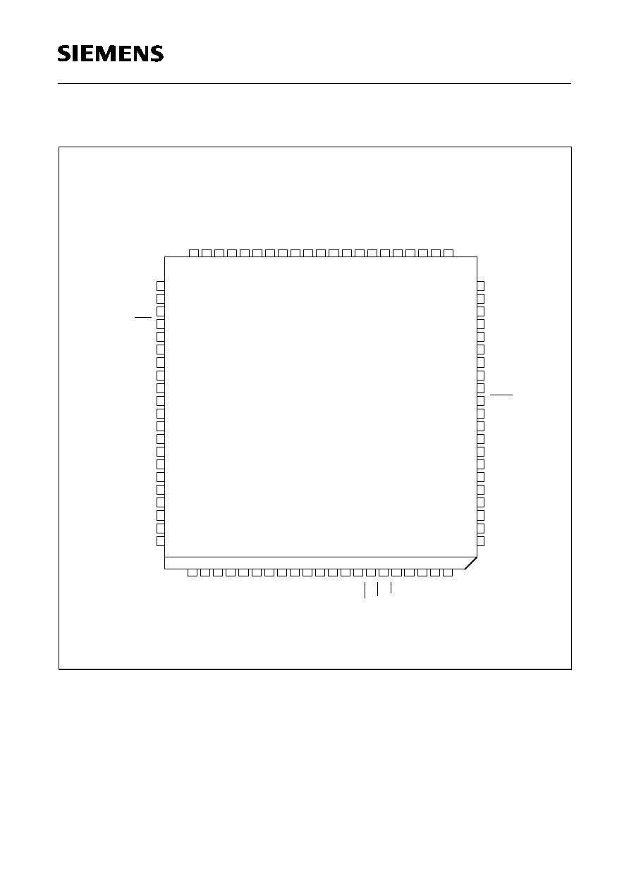
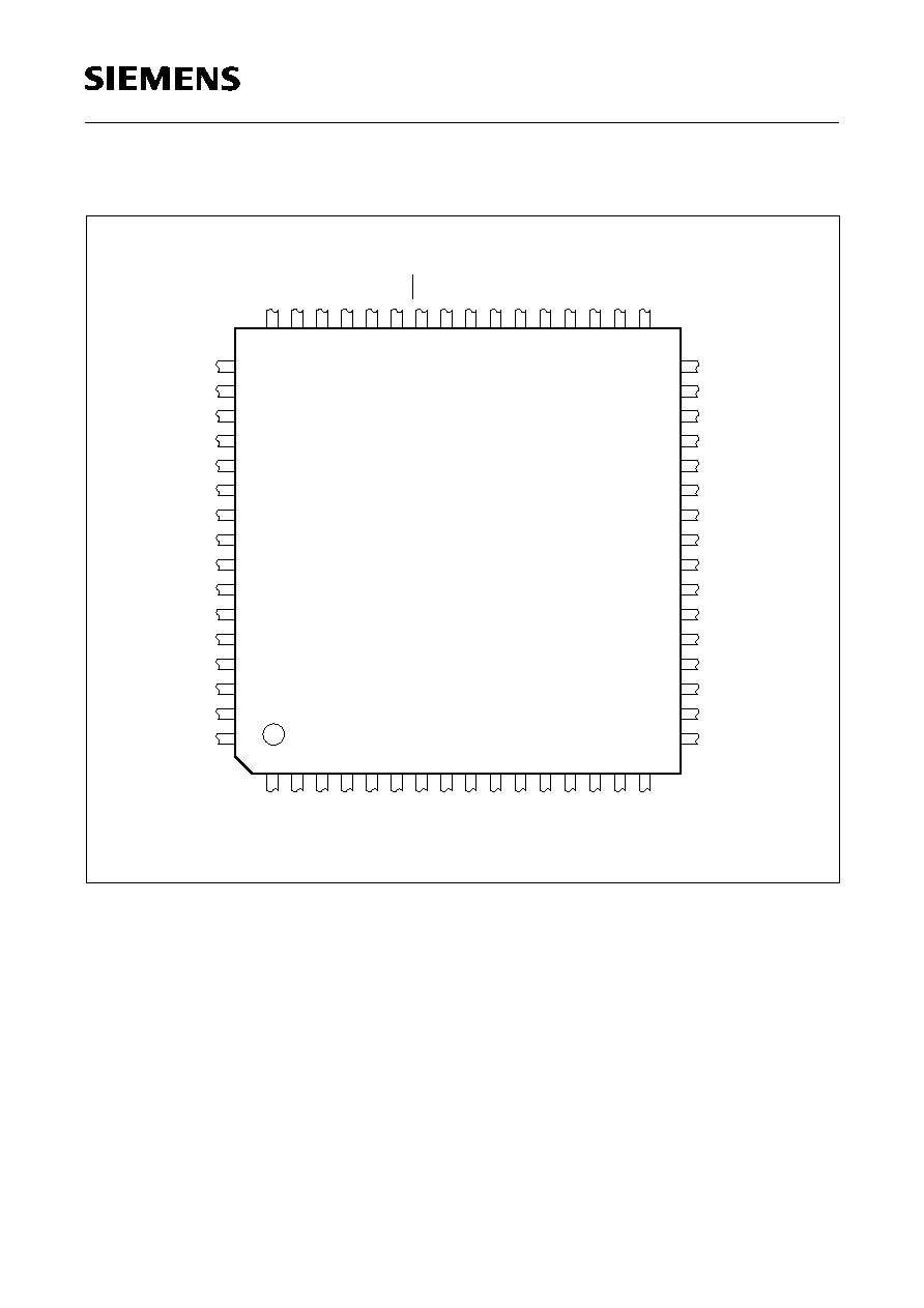
4.2
P-LCC-84-2, Emulator-Version (top view)
Figure 3
Differences compared to SDA 525x according to preliminary specification 06/96:
1. RGB-outputs deliver a current instead of a voltage (Pins 37, 38, 39).
2. Instead of FIL1SLC/FIL2SLC/FIL3SLC only FIL3 is needed with changed external
device dimensions (Pin 63). Former FIL1SLC and FIL2SLC remain "not connected"
(Pins 64, 65).
3. LCIN and LCOUT are not needed any more and remain "not connected" (Pins 44, 45).
`n. c.' = `not connected' means: Pins must be left open.
UEP09856
N.C.
D5
D0
D6
A0
D7
A1
A2
A10
A3
PSEN
32
D4
D1
33
D3
D2
COR
B
BLAN
N.C.
A14
A6
A4
A11
A5
A9
A8
A7
A13
A12
A16
12
11
A17/P4.0
ALE
RD
XTAL2
WR
RST
XTAL1
2
84
P0.4
HS/SC
VS/P4.7/ODD-EVEN
P0.0
P0.1
P0.2
P0.3
P0.6
54
P0.5
P0.7
STOP_OCF
ENE
P2.3/ANA3
P2.2/ANA2
P2.0/ANA0
FIL3
P3.0/ODD-EVEN
P1.2
P1.3
P1.4
P1.5
P1.6
P1.7
P3.3
CVBS
N.C.
N.C.
P3.7
P3.6
P3.5
P3.4
P3.1
75
74
P3.2
SDA 5250-2
34
35
36
37
38
39
40
41
42
43
44
45
46
47
48
49
50
51
52
53
73
72
71
70
69
68
67
66
65
64
63
62
61
60
59
58
57
56
55
10
9
8
7
6
5
4
3
83
82
81
80
79
78
77
76
1
13
14
15
16
17
18
19
20
21
22
23
24
25
26
27
28
29
30
31
A15
SS
V
G
R
SSA
V
P2.1/ANA1
SS
V
A18/P4.1
P1.1
P1.0
DD
V
DDA
V
REF
I
DD
V
SDA 525X-2
Semiconductor Group
9
1998-10-08
4.3
P-SDIP-52-1, ROM-Versions (top view)
Figure 4
Differences compared to SDA 525x according to preliminary specification 06/96:
1. RGB-outputs deliver a current instead of a voltage (Pins 47, 48, 49).
2. Instead of FIL1SLC/FIL2SLC/FIL3SLC only FIL3 is needed with changed external
device dimensions (Pin 25). Former FIL1SLC and FIL2SLC remain "not connected"
(Pins 26, 27).
3. LCIN and LCOUT are not needed any more and remain "not connected" (Pins 38, 39).
`n. c.' = `not connected' means: Pins must be left open.
UEP09857
P3.0
COR
38
30
29
15
RST
P3.7
P3.6
I
REF
V
SS
DD
1
2
3
4
5
6
7
8
9
10
42
41
40
39
P3.2
P0.0
P0.1
P0.2
VS/P4.7
P0.3
R
P0.4
G
P0.5
B
P0.6
BLAN
P0.7
P3.1
P3.5
V
XTAL1
P4.0
14
13
12
11
43
44
45
46
47
48
28
27
21
17
18
19
20
16
22
25
24
23
26
31
36
32
33
34
35
37
51
50
49
52
XTAL2
N.C.
P1.2
P1.1
P1.0
P1.7
P1.6
P1.5
P1.4
P1.3
FIL3
V
SS
N.C.
P3.4
HS/SC
P3.3
CVBS
P2.0
P2.1
P2.2
P2.3
N.C.
DD
V
SSA
V
N.C.
V
DDA
SDA 5251-2
SDA 5252-2
SDA 5254-2
SDA 5255-2
SDA 5256-2
SDA 5257-2
SDA 525X-2
Semiconductor Group
10
1998-10-08
4.4
P-MQFP-64-1, ROM-Versions (top view)
Figure 5
Differences compared to SDA 525x according to preliminary specification 06/96:
1. RGB-outputs deliver a current instead of a voltage (Pins 19, 20, 21).
2. Instead of FIL1SLC/FIL2SLC/FIL3SLC only FIL3 is needed with changed external
device dimensions (Pin 55). Former FIL1SLC and FIL2SLC remain "not connected"
(Pins 56, 57).
3. LCIN and LCOUT are not needed any more and remain "not connected" (Pins 7, 8).
`n. c.' = `not connected' means: Pins must be left open.
UEP10218
39
XTAL1
10
P3.6
P2.2
N.C.
P2.1
P2.3
CVBS
P3.3
62
64
63
1
61
60
59
2
3
4
N.C.
P3.7
N.C.
6
5
7
8
9
FIL3
N.C.
N.C.
P1.0
P1.1
P1.2
P1.3
55
57
58
56
54
53
52
P1.5
47
48
51
50
49
45
46
P1.6
N.C.
42
43
44
N.C.
P1.7
RST
40
41
P4.0
XTAL2
P3.5
N.C.
N.C.
P3.4
P3.2
13
11 12
14 15
HS/SC
19
17
18
16
20
21
22
R
N.C.
VS/P4.7
G
B
BLAN
36
37
38
34
35
P0.0
26
23
24
25
27
28
29
P0.7
P3.0
COR
P3.1
P0.6
P0.5
P0.4
33
30
32
31
P0.1
P0.3
P0.2
SS
V
V
SS
V
DD
V
DD
P2.0
N.C.
V
DD
V
DD
V
SS
V
SS
P1.4
SSA
V
DDA
V
N.C.
I
REF
SDA 5251M-2
SDA 5252M-2
SDA 5254M-2
SDA 5255M-2
SDA 5256M-2
SDA 5257M-2
SDA 525X-2
Semiconductor Group
11
1998-10-08
5
Pin Correspondence
Table 1
Pin Correspondence P-SDIP-52-1, P-MQFP-64-1, P-MQFP-80-1, P-MQFP-80-1,
P-LCC-84-2
Symbol
Pin No.
P-SDIP-52-1
Pin No.
P-MQFP-64-1
Pin No.
P-MQFP-80-1
Pin No.
P-MQFP-80-1
Pin No.
P-LCC-84-2
Changes compared
to SDA 525x
P0.0
P0.1
P0.2
P0.3
P0.4
P0.5
P0.6
P0.7
9
8
7
6
5
4
3
2
34
33
31
30
29
28
27
26
56
57
58
59
60
61
62
63
58
59
60
61
62
63
64
65
48
49
50
51
52
53
54
55
P1.0
P1.1
P1.2
P1.3
P1.4
P1.5
P1.6
P1.7
23
22
21
20
19
18
17
16
53
52
51
50
48
47
46
44
11
10
9
8
7
6
5
4
13
12
11
10
9
8
7
6
84
83
82
81
80
79
78
77
P2.0
P2.1
P2.2
P2.3
34
33
32
31
1
63
62
61
67
66
65
64
69
68
67
66
61
60
59
58
XTAL2
13
40
14
16
3
6 MHz crystal
XTAL1
12
39
15
17
4
6 MHz crystal
RST
15
42
16
18
5
V
DD
V
SS
11, 37
10, 35
5, 6, 37, 38
2, 3, 35, 36
13, 51
12, 50
15, 53
14, 52
2, 43
1, 42
R
G
B
BLAN
COR
47
48
49
50
51
19
20
21
22
23
45
46
47
48
49
47
48
49
50
51
37
38
39
40
41
current output
current output
current output
P3.0
P3.1
P3.2
P3.3
P3.4
P3.5
P3.6
P3.7
52
1
44
36
43
42
41
40
24
25
15
4
14
13
10
9
3
2
80
79
78
77
76
75
5
4
2
1
80
79
78
77
76
75
74
73
72
71
70
69
SDA 525X-2
Semiconductor Group
12
1998-10-08
LCIN and LCOUT are not needed any longer.
HS/SC
VS/P4.7/
ODD-EVEN
CVBS
45
46
30
16
18
60
54
55
74
56
57
76
46
47
68
New ext. comp.
values
I
REF
29
59
73
75
67
New ext. comp.
values
V
DDA
V
SSA
28
24
58
24
72
68
74
70
66
62
FIL3
25
55
69
71
63
New ext. comp.
values, FIL1/2 not
needed
P4.0
14
41
18
20
9
Table 1
Pin Correspondence P-SDIP-52-1, P-MQFP-64-1, P-MQFP-80-1, P-MQFP-80-1,
P-LCC-84-2 (cont'd)
Symbol
Pin No.
P-SDIP-52-1
Pin No.
P-MQFP-64-1
Pin No.
P-MQFP-80-1
Pin No.
P-MQFP-80-1
Pin No.
P-LCC-84-2
Changes compared
to SDA 525x
SDA 525X-2
Semiconductor Group
13
1998-10-08
Additional Pin Correspondence P-MQFP-80-1 and P-LCC-84-2
Table 2
Pin Correspondence P-MQFP-80-1, P-MQFP-80-1, P-LCC-84-2
Symbol
Pin No.
P-MQFP-80-1
Pin No.
P-MQFP-80-1
Pin No.
P-LCC-84-2
Changes vs. SDA 525x
A0
A1
A2
A3
A4
A5
A6
A7
A8
A9
A10
A11
A12
A13
A14
A15
A16
37
35
34
32
31
29
27
25
26
28
33
30
23
24
22
21
19
39
37
36
34
33
31
29
27
28
30
35
32
25
26
24
23
21
29
27
26
24
22
20
18
16
17
19
25
21
14
15
13
12
10
D0
D1
D2
D3
D4
D5
D6
D7
39
41
43
44
42
40
38
36
41
43
45
46
44
42
40
38
31
33
35
36
34
32
30
28
STOP_OCF
ENE
RD
WR
ALE
PSEN
�
�
52
53
17
1
�
�
54
55
19
3
56
57
7
6
8
23
new for MQFP
new for MQFP
new for MQFP
P4.1
20
22
11

SDA 525X-2
Semiconductor Group
14
1998-10-08
6
Differences of SDA 525x-2 Compared to SDA 525x
This delta specification describes the differences of the SDA 525x-2 compared to the
SDA 525x as described in the preliminary data sheet 1997-09-01.
6.1
Hardware-Compatibility
TVT-2 is pin-compatible to previous versions of TVT. However, some variations in
external components become necessary (see Application Circuit in Chapter 10):
1. The LC-oscillator is not necessary any longer.
2. The filters 1 and 2 are not needed any longer. Only filter 3 is needed but with different
external device dimensions.
3. Since the RBG outputs deliver a current, a voltage divider can be replaced by a single
resistor (see TVText Design Guide).
4. The external crystal is now 6 MHz instead of 18 MHz.
5. The CVBS-pin needs different dimensioning of the external components due to
changes in the internal clamping circuit.
6. The Iref-pin needs different dimensioning of the external components and an
additional blocking capacitor.
7. To avoid clock cross-talk and to improve the slicer performance use filter circuits at
the power supply pins to decouple digital and analog supplies.
8. Due to a reworked analog concept with the advantage of a more stable circuits and
better performance the power consumption has increased. For the Romless version
a maximum overall IDD-current of 95mA can be reached, for ROM versions up to
100mA.
Furthermore, the MQFP-80-packages now have RD, WR, and PSEN pins to connect to
external RAM.
6.2
Software-Compatibility
Only slight software changes may be necessary due to some register changes (see
chapter 7).
6.3
Improved Performance Sync- and Data-Slicer
Due to crystal locked PLLs the robustness of the sync- and data-slicer is improved.
6.4
Crystal-locked Display-PLL
The display clock will be locked to the internal PLL locked to the single external
6-MHz-crystal and, by this, will have very low jitter. Furthermore, the display width will
not vary. Procedures to adjust the display clock have to be disabled.
6.5
Improved Interface to External RAM
The SDA 5250M-2 (ROMless version P-MQFP-80-1) can also be used with external
RAM, because the pins RD, WR and PSEN are available. Furthermore, optional banking
SDA 525X-2
Semiconductor Group
15
1998-10-08
of external XDATA-memory will be possible, controlled by A16, A17, A18. This offers a
maximum of flexibility for 128-page-acquisition (see separate application note).
6.6
No UART
As described already in the errata sheet 03/97, release 1.0, the newer versions of the
SDA 525x and the SDA 525x-2 will not support a serial port (UART) any more.
6.7
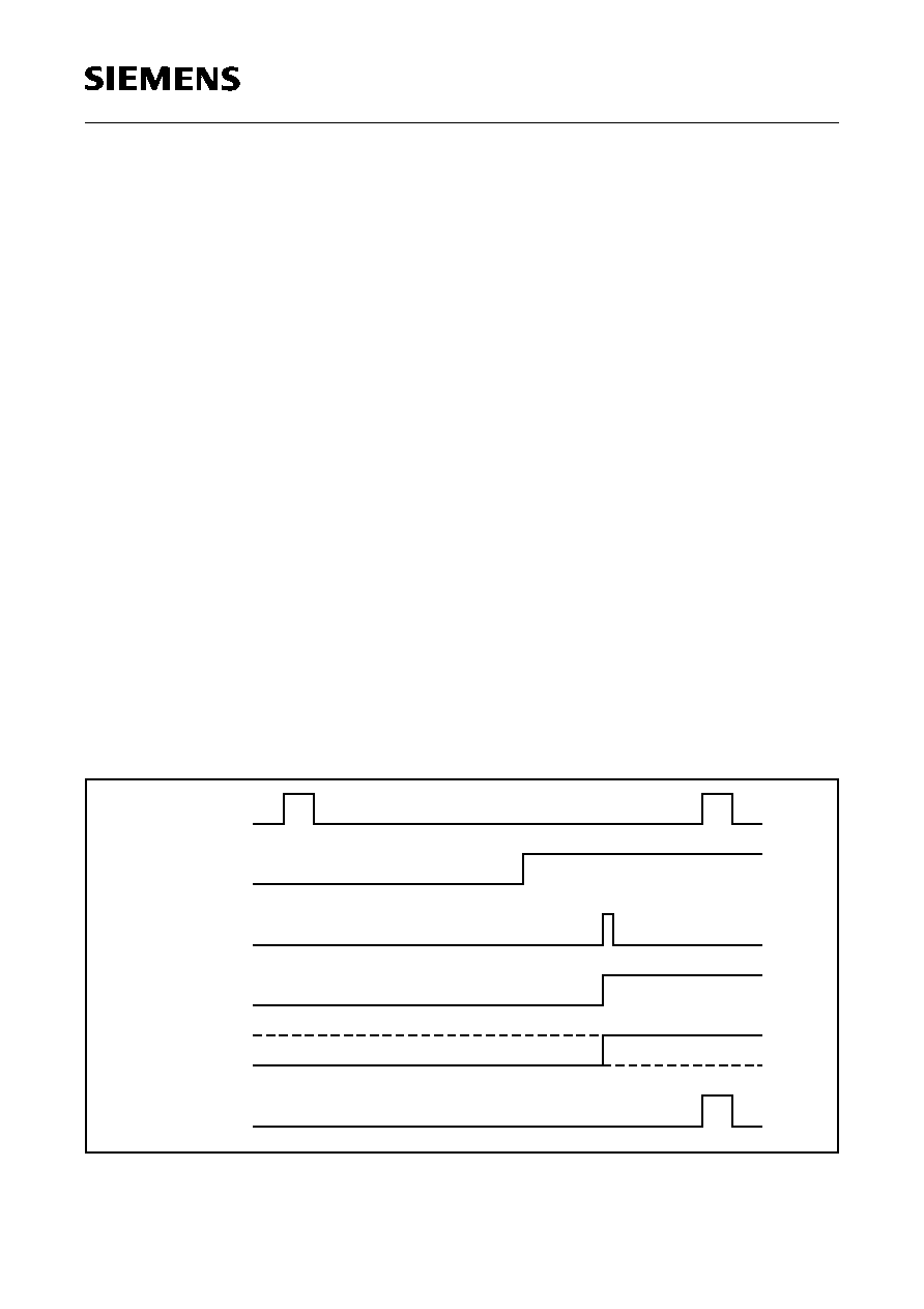
VS Sampling
The internal sampling time of the vertical sync pulse coming from either the VS pin or
from the sandcastle signal applied at the pin HS/SC is most important for a stable
display. Because the VSYNC inside a TV set is often delayed by external components,
the real relation-chip of the VS-phase and the appropriate picture frame may get lost.
The sampling time of the SDA 525x is derived from an internal display signal which can
only be modified by programming different horizontal offset values (DHD-Register). This
has the side-effect that depending on the desired horizontal offset the sampling point is
also varied and may show an unstable display. To avoid this dependency, the
SDA 525x-2 has a separate register to determine the VS sampling point with respect to
the HS pulse, which may be varied over a whole line in steps of 8
�
s. External
components for VS delaying are no more necessary and can be removed if the
programmed VS sampling points fits to the external timing between HS, VS and the
actual frame (even/odd). To get a better timing resolution in 100 Hz-applications a
special bit has been implemented to reduce the intervals between the possible sampling
points from 8 to 4
�
s. The register bits are described below. The following diagram shows
the internal VS processing in principle.
Figure 6
Internal VS Processing
HS
VS
Sample Point
Sampled VS
Field
Internal VS
UED11012
SDA 525X-2
Semiconductor Group
16
1998-10-08
Default after reset: 02
H
DAFR1
SFR Address B1
H
Following table gives an overview of the sampling point equivalents of the SDA 525x and
the SDA 525x-2 at a selected pixel frequency of 12 MHz.
(MSB)
(LSB)
-
-
-
-
VS100
VD.2
VD.1
VD.0
Bit 7 ... 4
Must be set to 0
VD
Vertical Delay: Reset value 0010, corresponds to 20
microsecond delay.
If VS100 = 0, delay can be set to 4, 12, 20, 28, 36, 44, 52,
60
�
s
If VS100 = 1, delay can be set to 2, 6, 10, 14, 18, 22, 26, 30
�
s
VS100
For VD bits selects the sampling mode
0 = 50 Hz
1 = 100 Hz
Sample Point in
�
s Equivalent DHD-Setup
for SDA 525x (decimal)
Equivalent Register Setup for
SDA 525x-2 (binary)
4
12
20
28
36
44
52
60
not possible
207
111
15
not possible
not possible
not possible
not possible
000
001
010
011
100
101
110
111
SDA 525X-2
Semiconductor Group
17
1998-10-08
6.8
RGB and Blanking Skew
In some applications the BLANK line is delayed by external components and/or special
video ICs and thus gets a delay with respect to the RGB- and COR lines which corrupts
the display by means of white and black vertical stripes at the beginning and at the end
of an OSD menu. To reduce this skew to an acceptable value, the RGB- and COR-lines
can be delayed by multiple of a pixel duration.
Default after reset: 00
H
DAFR2
SFR Address B2
H
(MSB)
(LSB)
-
-
-
-
-
-
RGBD.1
RGBD.0
Bit 7 ... 2
Must be set to 0
RGBD1 ... 0
= 00
= 01
= 10
= 11
RGB Delay in pixels counts
No delay
one pixel delay
two pixels delay
three pixel delay
SDA 525X-2
Semiconductor Group
18
1998-10-08
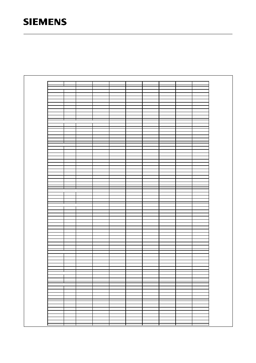
7
Registers of SDA 525x-2
It is very important, that registers not named or marked by "
xxxx
" here may in no case
be used in any way!
continued on next page ...
Register SDA 525x-2
Name
Address
Bit7
Bit6
Bit5
Bit4
Bit3
Bit2
Bit1
Bit0
Common Functions
AFR
A6
CDC
WDT
0
0
0
0
0
0
ACC
E0
ACC.7
ACC.6
ACC.5
ACC.4
ACC.3
ACC.2
ACC.1
ACC.0
B
F0
B.7
B.6
B.5
B.4
B.3
B.2
B.1
B.0
PSW
D0
CY
AC
F0
RS1
RS0
OV
F1
P
SP
81
SP.7
SP.6
SP.5
SP.4
SP.3
SP.2
SP.1
SP.0
DPH
83
DPH.7
DPH.6
DPH.5
DPH.4
DPH.3
DPH.2
DPH.1
DPH.0
DPL
82
DPL.7
DPL.6
DPL.5
DPL.4
DPL.3
DPL.2
DPL.1
DPL.0
DPSEL
A2
DPSEL.2
DPSEL.1
DPSEL.0
PCON
87
SMOD
PDS
IDLS
PDE
IDLE
Emulation Functions (Emulation Version only)
EMREG
FE
EM.7
EM.6
EM.5
EM.4
EM.3
EM.2
EM.1
EM.0
Acquisition
ACQSIR
C0
EVENEN
EVENST
LIN24EN
LIN24ST
AVIREN
AVIRST
AHIREN
AHIRST
ACQMS1
C1
OSDACQ
WSSE
VPSE
NTSC
CRIC.1
CRIC.0
ENERT
TTXE
ACQMS2
C2
TEST.4
TEST.3
TEST.2
TEST.1
TEST.0
Display Generator
DHD
C3
HD.7
HD.6
HD.5
HD.4
HD.3
HD.2
HD.1
HD.0
DVD
C4
VD.5
VD.4
VD.3
VD.2
VD.1
VD.0
DTCR
C5
CORI
CORO
ICRP
IBP
TRFI
TRFO
TRBI
TRBO
DMODE1
C6
ST_TOP
ST_DIS
CON
DH.1
DH.0
BD_24
BD_1_23
BD_0
DMODE2
C7
DCHAP.2
DCHAP.1
DCHAP.0
C10
C7
TTXSIR
C8
VSY
HSY
PCLK
DVIREN
DVIRST
DHIREN
DHIRST
LANGC
C9
OSD_64
LANGC.6
LANGC.5
LANGC.4
LANGC.3
LANGC.2
LANGC.1
LANGC.0
DCCP
CA
DC_EN
DCCP:5
DCCP.4
DCCP:6
DCCP.5
DCCP:7
DCCP.6
DCRP
CB
TRBOS
COROS
DCRP.4
DCRP.3
DCRP.2
DCRP.1
DCRP.0
DTIM
CC
BG_R
BG_G
BG_B
EO_P30
EO_VS
SANDC
LIN9
LIN8
SCCON
CE
CORTM
SCCH.2
SCCH.1
SCCH.0
FL5MX
SCCL.2
SCCL.1
SCCL.0
DMOD
D6
BG_MODE
VPS_TM
HG_MOD
DH_MODE
DSDW
Analog to Digital Converter
ADCON
D8
xxxx
xxxx
IADC
BSY
ADM
0
MX1
MX0
ADDAT
D9
AD7
AD6
AD5
AD4
AD3
AD2
AD1
AD0
DAPR
DA
Pulse Width Modulator
PWME
F8
E7
E6
E5
E4
E3
E2
E1
E0
PWCL
F7
PWCL.7
PWCL.6
PWCL.5
PWCL.4
PWCL.3
PWCL.2
PWCL.1
PWCL.0
PWCH
F9
PWCH.7
PWCH.6
PWCH.5
PWCH.4
PWCH.3
PWCH.2
PWCH.1
PWCH.0
PWCOMP0
F1
COMP0.7
COMP0.6
COMP0.5
COMP0.4
COMP0.3
COMP0.2
COMP0.1
COMP0.0
PWCOMP1
F2
COMP1.7
COMP1.6
COMP1.5
COMP1.4
COMP1.3
COMP1.2
COMP1.1
COMP1.0
PWCOMP2
F3
COMP2.7
COMP2.6
COMP2.5
COMP2.4
COMP2.3
COMP2.2
COMP2.1
COMP2.0
PWCOMP3
F4
COMP3.7
COMP3.6
COMP3.5
COMP3.4
COMP3.3
COMP3.2
COMP3.1
COMP3.0
PWCOMP4
F5
COMP4.7
COMP4.6
COMP4.5
COMP4.4
COMP4.3
COMP4.2
COMP4.1
COMP4.0
PWCOMP5
F6
COMP5.7
COMP5.6
COMP5.5
COMP5.4
COMP5.3
COMP5.2
COMP5.1
COMP5.0
PWCOMP6
FB
COMP6.7
COMP6.6
COMP6.5
COMP6.4
COMP6.3
COMP6.2
COMP6.1
COMP6.0
PWEXT6
FA
EXT6.7
EXT6.6
EXT6.5
EXT6.4
EXT6.3
EXT6.2
EXT6.1
EXT6.0
PWCOMP7
FD
COMP7.7
COMP7.6
COMP7.5
COMP7.4
COMP7.3
COMP7.2
COMP7.1
COMP7.0
PWEXT7
FC
EXT7.7
EXT7.6
EXT7.5
EXT7.4
EXT7.3
EXT7.2
EXT7.1
EXT7.0
Port Functions
P0
80
P0.7
P0.6
P0.5
P0.4
P0.3
P0.2
P0.1
P0.0
P1
90
P1.7
P1.6
P1.5
P1.4
P1.3
P1.2
P1.1
P1.0
P2
A0
P2.3
P2.2
P2.1
P2.0
P3
B0
P3.7
P3.6
P3.5
P3.4
P3.3
P3.2
P3.1
P3.0
P4
E8
P4.1
P4.0
Serial Interface
SCON
98
xxxx
xxxx
xxxx
xxxx
xxxx
xxxx
xxxx
xxxx
SBUF
99
xxxx
xxxx
xxxx
xxxx
xxxx
xxxx
xxxx
xxxx
Interrupt Controller
IE
A8
EA
EADC
ETSI
xxxx
ETI
EX1
ET0
EX0
IP0
A9
IP0.6
IP0.5
IP0.4
IP0.3
IP0.2
IP0.1
IP0.0
IP1
AA
IP1.6
IP1.5
IP1.4
IP1.3
IP1.2
IP1.1
IP1.0
IRCON
AB
EX1R
EX1F
EX0R
EX0F
Timer 0/1
TMOD
89
GATE
C/T
M1
M0
GATE
C/T
M1
M0
TCON
88
TF1
TR1
TF0
TR0
IE1
IT1
IE0
IT0
TH1
8D
TH1.7
TH1.6
TH1.5
TH1.4
TH1.3
TH1.2
TH1.1
TH1.0
TH0
8C
TH0.7
TH0.6
TH0.5
TH0.4
TH0.3
TH0.2
TH0.1
TH0.0
TL1
8B
TL1.7
TL1.6
TL1.5
TL1.4
TL1.3
TL1.2
TL1.1
TL1.0
TL0
8A
TL0.7
TL0.6
TL0.5
TL0.4
TL0.3
TL0.2
TL0.1
TL0.0
SDA 525X-2
Semiconductor Group
19
1998-10-08
Differences compared to SDA 525x according to preliminary specification 06/96:
1. The serial interface is not supported any longer. By this, registers SCON and SBUF
are no longer available. The "Serial Interrupt Enable Flag" ES of the Interrupt Enable
register (Bit 4 of A8) must not be written (default after reset = 0).
2. The functions and bits Prescaler Control (PSC) and ADC sample time (STADC) of the
Special Function Register ADCON are not available any more. Bits 7 and 6 of D8 must
be 0.
3. The registers following must not be written. The software needs to be checked
accordingly.
SBUF (99):
Bits 0 to 7
SCON (98):
Bits 0 to 7
ACQMS2 (C2):
Bits 0 to 7
DMODE2 (C7):
Bits 5 to 7
ADCON (D8):
Bits 6 and 7
IE (A8):
Bit 4
The allowed bits of DMODE2, ADCON and IE have to be changed with the commands
ANL or ORL.
Register SDA 525x-2
Name
Address
Bit7
Bit6
Bit5
Bit4
Bit3
Bit2
Bit1
Bit0
Watchdog Timer
WDCON
A7
WDTS
SWDT
WDTREL
86
WDTREL.7
WDTREL.6
WDTREL.5
WDTREL.4
WDTREL.3
WDTREL.2
WDTREL.1
WDTREL.0
WDTL
84
WDTL.7
WDTL.6
WDTL.5
WDTL.4
WDTL.3
WDTL.2
WDTL.1
WDTL.0
WDTH
85
WDTH.7
WDTH.6
WDTH.5
WDTH.4
WDTH.3
WDTH.2
WDTH.1
WDTH.0
Infrared Capture-/Compare Timer
RELL
E1
RELL.7
RELL.6
RELL.5
RELL.4
RELL.3
RELL.2
RELL.1
RELL.0
RELH
E2
RELH.7
RELH.6
RELH.5
RELH.4
RELH.3
RELH.2
RELH.1
RELH.0
CAPL
E3
CAPL.7
CAPL.6
CAPL.5
CAPL.4
CAPL.3
CAPL.2
CAPL.1
CAPL.0
CAPH
E4
CAPH.7
CAPH.6
CAPH.5
CAPH.4
CAPH.3
CAPH.2
CAPH.1
CAPH.0
IRTCON
E5
OV
PR
PLG
REL
RUN
RISE
FALL
SEL
Memory Management Unit (ROM-less versions only)
MEX1
94
CB18
CB17
CB16
NB18
NB17
NB16
MEX2
95
MM
MB18
MB17
MB16
SF
IB18
IB17
IB16
=
Register Bit read-only
xxxx
=
Register Bit not available
=
Register Bit write-only
and not needed any longer
SDA 525X-2
Semiconductor Group
20
1998-10-08
7.1
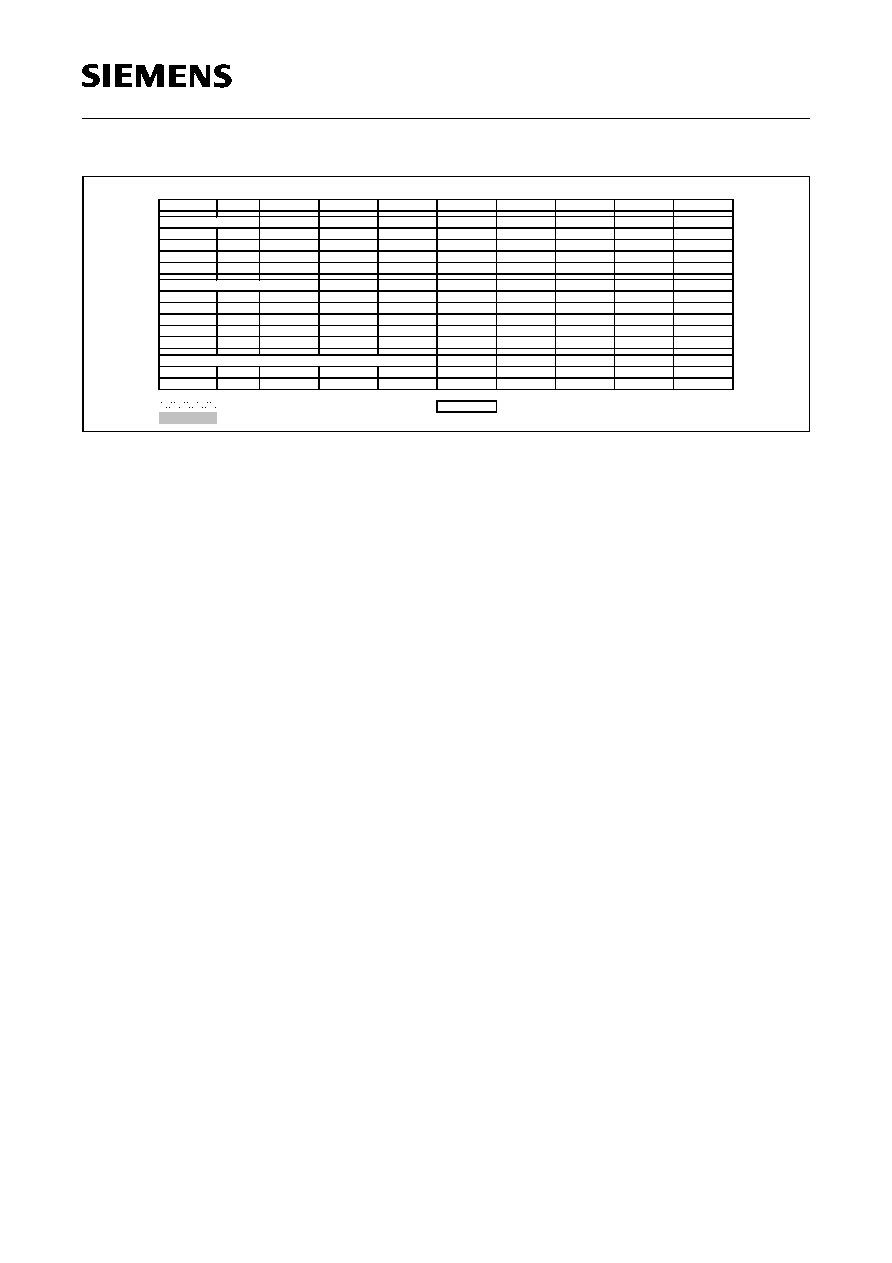
Address Space of SDA 525x-2
The registers of the SDA 525x-2 sorted by address are listed in the table following:
The address space for MOVX is distributed as follows:
0000 - 7FFF: reserved for external SRAM (32k)
8000 - 9FFF: reserved for future extensions (8k)
A000 - BFFF: read access to Pixel-ROM via MOVX-command (8k)
C000 - DFFF: display-chapters 1 to 8 (8k)
E000 - E7FF: display-chapters 9 and 10 (2k)
(optional)
Register SDA 525x-2 sorted by address
Address
Name
Address
Bit7
Bit6
Bit5
Bit4
Bit3
Bit2
Bit1
Bit0
decimal
hex
128
P0
80
P0.7
P0.6
P0.5
P0.4
P0.3
P0.2
P0.1
P0.0
129
SP
81
SP.7
SP.6
SP.5
SP.4
SP.3
SP.2
SP.1
SP.0
130
DPL
82
DPL.7
DPL.6
DPL.5
DPL.4
DPL.3
DPL.2
DPL.1
DPL.0
131
DPH
83
DPH.7
DPH.6
DPH.5
DPH.4
DPH.3
DPH.2
DPH.1
DPH.0
132
WDTL
84
WDTL.7
WDTL.6
WDTL.5
WDTL.4
WDTL.3
WDTL.2
WDTL.1
WDTL.0
133
WDTH
85
WDTH.7
WDTH.6
WDTH.5
WDTH.4
WDTH.3
WDTH.2
WDTH.1
WDTH.0
134
WDTREL
86
WDTREL.7
WDTREL.6
WDTREL.5
WDTREL.4
WDTREL.3
WDTREL.2
WDTREL.1
WDTREL.0
135
PCON
87
SMOD
PDS
IDLS
PDE
IDLE
136
TCON
88
TF1
TR1
TF0
TR0
IE1
IT1
IE0
IT0
137
TMOD
89
GATE
C/T
M1
M0
GATE
C/T
M1
M0
138
TL0
8A
TL0.7
TL0.6
TL0.5
TL0.4
TL0.3
TL0.2
TL0.1
TL0.0
139
TL1
8B
TL1.7
TL1.6
TL1.5
TL1.4
TL1.3
TL1.2
TL1.1
TL1.0
140
TH0
8C
TH0.7
TH0.6
TH0.5
TH0.4
TH0.3
TH0.2
TH0.1
TH0.0
141
TH1
8D
TH1.7
TH1.6
TH1.5
TH1.4
TH1.3
TH1.2
TH1.1
TH1.0
144
P1
90
P1.7
P1.6
P1.5
P1.4
P1.3
P1.2
P1.1
P1.0
148
MEX1
94
CB18
CB17
CB16
NB18
NB17
NB16
149
MEX2
95
MM
MB18
MB17
MB16
SF
IB18
IB17
IB16
160
P2
A0
P2.3
P2.2
P2.1
P2.0
162
DPSEL
A2
DPSEL.2
DPSEL.1
DPSEL.0
166
AFR
A6
CDC
WDT
0
0
0
0
0
0
167
WDCON
A7
WDTS
SWDT
168
IE
A8
EA
EADC
ETSI
xxxx
ETI
EX1
ET0
EX0
169
IP0
A9
IP0.6
IP0.5
IP0.4
IP0.3
IP0.2
IP0.1
IP0.0
170
IP1
AA
IP1.6
IP1.5
IP1.4
IP1.3
IP1.2
IP1.1
IP1.0
171
IRCON
AB
EX1R
EX1F
EX0R
EX0F
176
P3
B0
P3.7
P3.6
P3.5
P3.4
P3.3
P3.2
P3.1
P3.0
192
ACQSIR
C0
EVENEN
EVENST
LIN24EN
LIN24ST
AVIREN
AVIRST
AHIREN
AHIRST
193
ACQMS1
C1
OSDACQ
WSSE
VPSE
NTSC
CRIC.1
CRIC.0
ENERT
TTXE
194
ACQMS2
C2
LIN5EN
LIN5ST
TEST.4
TEST.3
TEST.2
TEST.1
TEST.0
195
DHD
C3
HD.7
HD.6
HD.5
HD.4
HD.3
HD.2
HD.1
HD.0
196
DVD
C4
VD.5
VD.4
VD.3
VD.2
VD.1
VD.0
197
DTCR
C5
CORI
CORO
ICRP
IBP
TRFI
TRFO
TRBI
TRBO
198
DMODE1
C6
ST_TOP
ST_DIS
CON
DH.1
DH.0
BD_24
BD_1_23
BD_0
199
DMODE2
C7
DCHAP.2
DCHAP.1
DCHAP.0
C10
C7
200
TTXSIR
C8
VSY
HSY
PCLK
DVIREN
DVIRST
DHIREN
DHIRST
201
LANGC
C9
OSD_64
LANGC.6
LANGC.5
LANGC.4
LANGC.3
LANGC.2
LANGC.1
LANGC.0
202
DCCP
CA
DC_EN
DCCP:5
DCCP.4
DCCP:6
DCCP.5
DCCP:7
DCCP.6
203
DCRP
CB
TRBOS
COROS
DCRP.4
DCRP.3
DCRP.2
DCRP.1
DCRP.0
204
DTIM
CC
BG_R
BG_G
BG_B
EO_P30
EO_VS
SANDC
LIN9
LIN8
206
SCCON
CE
CORTM
SCCH.2
SCCH.1
SCCH.0
FL5MX
SCCL.2
SCCL.1
SCCL.0
208
PSW
D0
CY
AC
F0
RS1
RS0
OV
F1
P
214
DMOD
D6
BG_MODE
VPS_TM
HG_MOD
DH_MODE
DSDW
216
ADCON
D8
xxxx
xxxx
IADC
BSY
ADM
0
MX1
MX0
217
ADDAT
D9
AD7
AD6
AD5
AD4
AD3
AD2
AD1
AD0
218
DAPR
DA
224
ACC
E0
ACC.7
ACC.6
ACC.5
ACC.4
ACC.3
ACC.2
ACC.1
ACC.0
225
RELL
E1
RELL.7
RELL.6
RELL.5
RELL.4
RELL.3
RELL.2
RELL.1
RELL.0
226
RELH
E2
RELH.7
RELH.6
RELH.5
RELH.4
RELH.3
RELH.2
RELH.1
RELH.0
227
CAPL
E3
CAPL.7
CAPL.6
CAPL.5
CAPL.4
CAPL.3
CAPL.2
CAPL.1
CAPL.0
228
CAPH
E4
CAPH.7
CAPH.6
CAPH.5
CAPH.4
CAPH.3
CAPH.2
CAPH.1
CAPH.0
229
IRTCON
E5
OV
PR
PLG
REL
RUN
RISE
FALL
SEL
232
P4
E8
P4.1
P4.0
240
B
F0
B.7
B.6
B.5
B.4
B.3
B.2
B.1
B.0
241
PWCOMP0
F1
COMP0.7
COMP0.6
COMP0.5
COMP0.4
COMP0.3
COMP0.2
COMP0.1
COMP0.0
242
PWCOMP1
F2
COMP1.7
COMP1.6
COMP1.5
COMP1.4
COMP1.3
COMP1.2
COMP1.1
COMP1.0
243
PWCOMP2
F3
COMP2.7
COMP2.6
COMP2.5
COMP2.4
COMP2.3
COMP2.2
COMP2.1
COMP2.0
244
PWCOMP3
F4
COMP3.7
COMP3.6
COMP3.5
COMP3.4
COMP3.3
COMP3.2
COMP3.1
COMP3.0
245
PWCOMP4
F5
COMP4.7
COMP4.6
COMP4.5
COMP4.4
COMP4.3
COMP4.2
COMP4.1
COMP4.0
246
PWCOMP5
F6
COMP5.7
COMP5.6
COMP5.5
COMP5.4
COMP5.3
COMP5.2
COMP5.1
COMP5.0
247
PWCL
F7
PWCL.7
PWCL.6
PWCL.5
PWCL.4
PWCL.3
PWCL.2
PWCL.1
PWCL.0
248
PWME
F8
E7
E6
E5
E4
E3
E2
E1
E0
249
PWCH
F9
PWCH.7
PWCH.6
PWCH.5
PWCH.4
PWCH.3
PWCH.2
PWCH.1
PWCH.0
250
PWEXT6
FA
EXT6.7
EXT6.6
EXT6.5
EXT6.4
EXT6.3
EXT6.2
EXT6.1
EXT6.0
251
PWCOMP6
FB
COMP6.7
COMP6.6
COMP6.5
COMP6.4
COMP6.3
COMP6.2
COMP6.1
COMP6.0
252
PWEXT7
FC
EXT7.7
EXT7.6
EXT7.5
EXT7.4
EXT7.3
EXT7.2
EXT7.1
EXT7.0
253
PWCOMP7
FD
COMP7.7
COMP7.6
COMP7.5
COMP7.4
COMP7.3
COMP7.2
COMP7.1
COMP7.0
254
EMREG
FE
EM.7
EM.6
EM.5
EM.4
EM.3
EM.2
EM.1
EM.0

SDA 525X-2
Semiconductor Group
21
1998-10-08
E800 - F3FF: reserved for future extensions (3k)
F400 - F7FF: VBI buffer (1k)
F800 - FBFF: CPU RAM (1k)
FC00- FFFF: reserved for future extensions (1k)
8
Software Changes
All calls of the subroutine "adjust_horizontal" (inside the module IFRDEMO.C51 on the
Firmware Demo Disk) must be removed from the external controller software. This
routine was developed to adjust the display to the middle of the screen according to
tolerances of the LC-oscillator. This oscillator is not used any more. The pixel clock is
derived from the single external crystal. However, customers who are using SDA 525x-2
without emulating with SDA 5250-2 or 5250M-2 need to use some adjustment routine for
their first circuits. As soon as the correct adjustment is known, it can be used as a fixed
value for initialization or for future software.
Furthermore, due to some changes in the special function registers, the software needs
to be checked. The changes are in detail:
1. The serial interface is not supported any longer. By this, registers SCON and SBUF
are no longer available. The "Serial Interrupt Enable Flag" ES of the Interrupt Enable
register (Bit 4 of A8) must not be written (default after reset = 0).
2. The functions and bits Prescaler Control (PSC) and ADC sample time (STADC) of the
Special Function Register ADCON are not available any more. Bits 7 and 6 of D8 must
be 0.
3. The registers following must not be written. The software needs to be checked
accordingly.
SBUF (99):
Bits 0 to 7
SCON (98):
Bits 0 to 7
ACQMS2 (C2):
Bits 0 to 7
DMODE2 (C7):
Bits 5 to 7
ADCON (D8):
Bits 6 and 7
IE (A8):
Bit 4
The allowed bits of DMODE2, ADCON and IE have to be changed with the commands
ANL or ORL.
9
Timing
Although the frequency of the external quarz is now 6 MHz, all the internal timings
correspond to that of the SDA525x with an 18 MHz quarz. This is achieved by an internal
PLL.
SDA 525X-2
Semiconductor Group
22
1998-10-08
10
Application Circuit
Use of SDA 525x-2 (Design Step B) as replacement for SDA 525x:
(For more detailed application hints refer to 'TVText Design Guide V1.5')
Figure 7
33 nF
2.7 k
+5 V
Only ROMless Versions
3 x 220
UED09862
F
SSA
V
V
DDA
REF
F
100 nF
27 k
H
�
10
10
�
COR
Blank
B
G
SS
V
DD
V
10
�
SC
FIL3
100 nF
�
10 H
+5 V
Sandcastle
10 k
10
+5 V
�
F
33 pF
6 MHz
33 pF
I/O Port 1 (PWM)
I/O Port 0 (Open-Drain)
I/O Port 3
Input Port 2 (ADC)
P2.0-7
P3.0-7
CVBS
SDA 525X-2
R
XTAL2
RST
8
A0-18
P0.0-7
P1.0-7
XTAL1
D0-7
A
D
EPROM
4
8
8
1 M
330 nF
CVBS
V
DDA
10 nF

SDA 525X-2
Semiconductor Group
23
1998-10-08
Necessary changes compared to SDA 525x according to preliminary data sheet
1998-02-18 are:
1. RGB-outputs deliver a current instead of a voltage. Any voltage divider can be
replaced by a single resistor. This resistor will have a different dimension. The nominal
output current is 5.2 mA with a resistor of 27 k
at the
I
REF
-pin.
2. Instead of FIL1SLC/FIL2SLC/FIL3SLC only FIL3 is needed with changed external
device dimensions. Former FIL1SLC and FIL2SLC remain "not connected". For best
slicer performance FIL3 is tied to
V
DDA
. FIL3 may be tied to
V
SSA
, if a ripple free
V
DDA
is available.
3. LCIN and LCOUT are not needed any more and are not connected or used for RD and
WR in the P-MQFP-80-1-package, respectively.
4. P-MQFP-80-1 now has RD (Pin 52), WR (53) and PSEN (1) Pins to connect external
RAM.
5. The 18-MHz-crystal is replaced by a 6-MHz type.
`n. c.' = `not connected' means: Pins must be left open.