
Data Sheet 1997-09-01
ICs for Consumer Electronics
MEGATEXT and MEGATEXT PLUS ICs
SDA 5273 / SDA 5275
SDA 5273-2 / SDA 5275-2
Data Classification
Maximum Ratings
Maximum ratings are absolute ratings; exceeding only one of these values may cause irreversible
damage to the integrated circuit.
Characteristics
The listed characteristics are ensured over the operating range of the integrated circuit. Typical
characteristics specify mean values expected over the production spread. If not otherwise specified,
typical characteristics apply at
T
A
= 25
∞
C and the given supply voltage.
Operating Range
In the operating range the functions given in the circuit description are fulfilled.
For detailed technical information about
"Processing Guidelines"
and
"Quality Assurance"
for
ICs, see our
"Short Form Catalog".
MEGATEXT
Æ
and MEGATEXT PLUS ICs
SDA 5273 / SDA 5275
SDA 5273-2 / SDA 5275-2
Revision History:
1997-09-01
Previous Releases:
11.96
Page
Subjects (changes since last revision)
20
Now also covers SDA 5275-2 and SDA 5273-2 versions;
Reset/chip initialization update
Published by
Siemens AG, Bereich Halbleiter, Marketing-Kommunikation,
Balanstraþe 73, 81541 M¸nchen
© Siemens AG 1997. All Rights Reserved.
As far as patents or other rights of third parties are concerned, liability is only assumed for components, not
for applications, processes and circuits implemented within components or assemblies.
The information describes the type of component and shall not be considered as assured characteristics.
Terms of delivery and rights to change design reserved.
For questions on technology, delivery and prices please contact the Semiconductor Group Offices in Ger-
many or the Siemens Companies and Representatives worldwide (see address list).
Due to technical requirements components may contain dangerous substances. For information on the
types in question please contact your nearest Siemens Office, Semiconductor Group.
Siemens AG is an approved CECC manufacturer.
Packing
Please use the recycling operators known to you. We can also help you - get in touch with your nearest
sales office. By agreement we will take packing material back, if it is sorted. You must bear the costs of
transport.
For packing material that is returned to us unsorted or which we are not obliged to accept, we shall have to
invoice you for any costs incurred.
Edition 1997-09-01

SDA 5273 / 75
SDA 5273-2 / 75-2
Semiconductor Group
3
1997-09-01
Contents
Page
1
Features
. . . . . . . . . . . . . . . . . . . . . . . . . . . . . . . . . . . . . . . . . . . . . . . . . . . . .4
1.1
Pin Definitions and Functions . . . . . . . . . . . . . . . . . . . . . . . . . . . . . . . . . . . . .6
1.2
Pin Definitions and Functions . . . . . . . . . . . . . . . . . . . . . . . . . . . . . . . . . . . . .9
2
Electrical Characteristics
. . . . . . . . . . . . . . . . . . . . . . . . . . . . . . . . . . . . . .12
3
Diagrams
. . . . . . . . . . . . . . . . . . . . . . . . . . . . . . . . . . . . . . . . . . . . . . . . . . . .21
4
Package Outlines
. . . . . . . . . . . . . . . . . . . . . . . . . . . . . . . . . . . . . . . . . . . . .29
MEGATEXT
Æ
is a registered trademark of Siemens AG
MEGATEXT
Æ
and MEGATEXT PLUS ICs
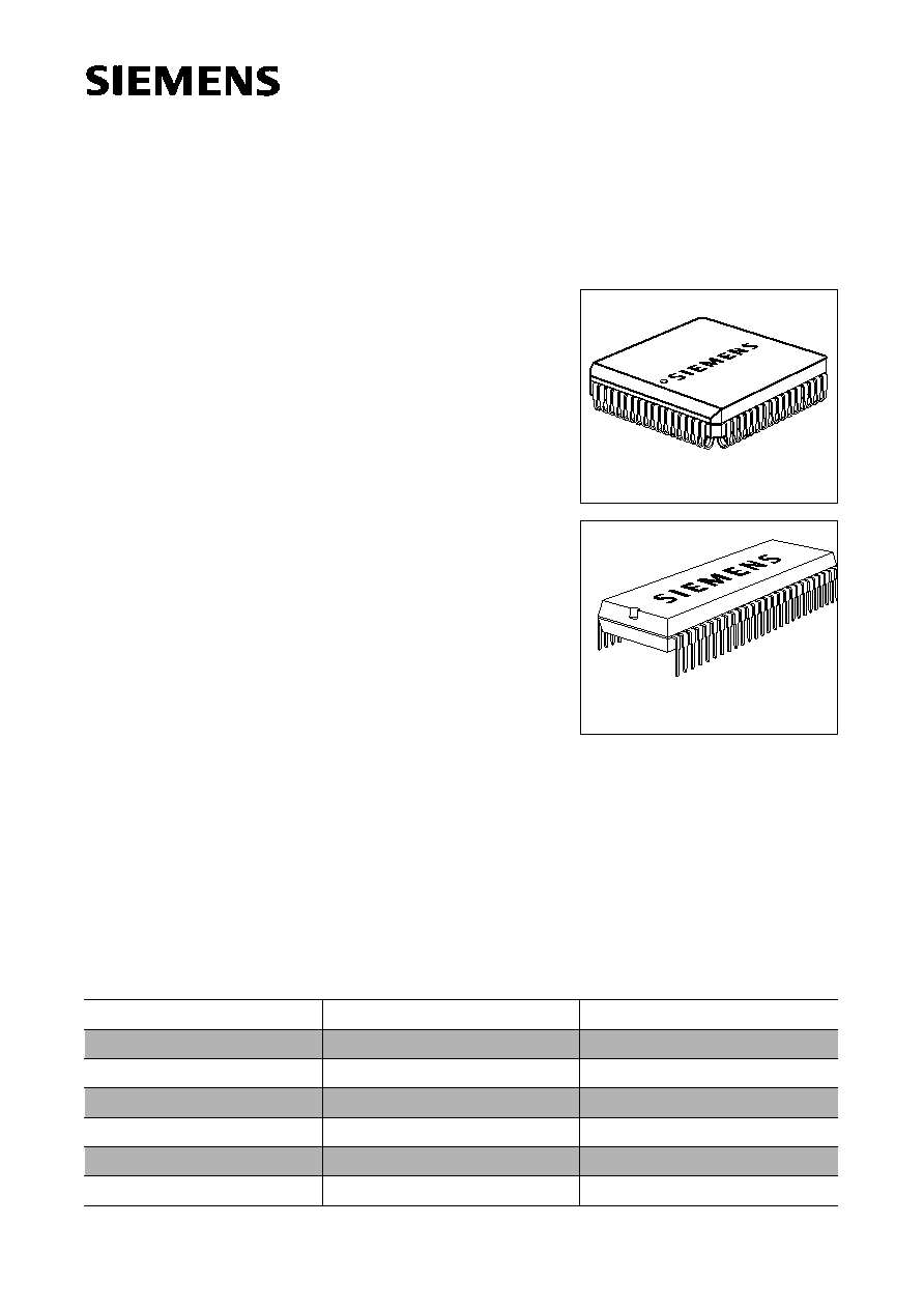
Preliminary Data
CMOS IC
SDA 5273 / 75
SDA 5273-2 / 75-2
P-LCC-68-1
P-SDIP-52-1
1
Features
q
Single chip teletext IC
q
Analog CVBS-input with onchip clamping circuitry
q
Slicer
q
Supports level 1, 2.5 and 3.5 ETSI teletext standard
q
Stores up to 14 teletext pages on chip
q
Stores up to 2048 teletext pages with external
16 M memory
q
SDA 5275: full level 2.5 processing
q
Analog RGB-output
q
41 latin script languages
q
12
◊
10 character size
q
Parallel display attributes
q
64 from 4096 colors selectable
q
Enhanced flash modes
q
Dynamically redefinable character set (DRCS, PCS)
q
Pixel graphics
q
Fullscreen display (64
◊
32 or 80
◊
24 character positions)
q
Horizontal and vertical scrolling
q
Graphic cursors
q
4:3 and 16:9 display
q
Multinorm display (50/60/100/120 Hz)
q
RISC-processor
q
Firmware downloadable
q
I
2
C / 3 wire UART-interface (1 Mbit/s)
q
Independent clocks for acquisition and display
q
Tools for greatly simplified software development
q
24-Kbyte on-chip reconfigurable DRAM
q
44160-bit character ROM
q
One external crystal for all standards
Type
Ordering Code
Package
SDA 5273 / 75 P
on request
P-LCC-68-1
SDA 5273 / 75 S
on request
P-SDIP-52-1
SDA 5273-2 / 75-2P
on request
P-LCC-68-1
SDA 5273-2 / 75-2S
on request
P-SDIP-52-1
SDA 5273C / 73-2C P
on request
P-LCC-68-1
SDA 5273C / 73-2C S
on request
P-SDIP-52-1
Semiconductor Group
4
1997-09-01
SDA 5273 / 75
SDA 5273-2 / 75-2
Semiconductor Group
5
1997-09-01
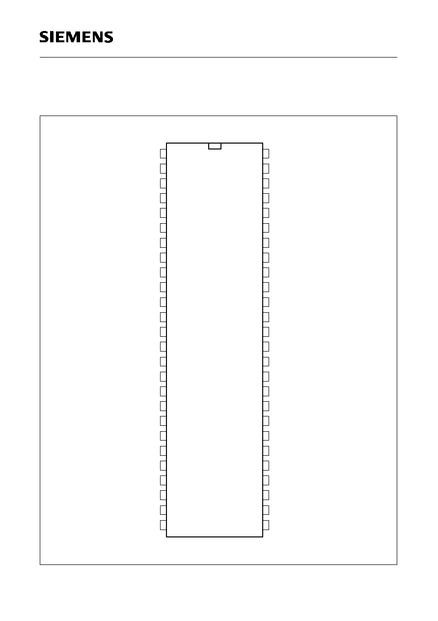
Pin Configuration
(top view)
UEP04657
10
9
8
7
6
5
4
3
2
1
12
11
27
28
13
14
V
DD
TM
GPO
OUT
HS
VS/VCS
15
16
17
18
19
20
36
35
34
33
32
31
30
29
40
39
38
37
CVBS
SDA
SCL
CORQ
BLAN
B
G
R
RGB-GND
CASQ
3
D
2
D
D0
D1
23
22
21
24
25
26
0
11
A
10
A
48
49
50
51
41
42
43
44
45
46
52
47
O
CLK-
TCSQ/FLD
XIN
X
1
2
NTQ
CEN
1
SS
V
A9
WEQ
RASQ
V
SSA 2
V
SS2
V
BB
V
SS3
V
SS4
A
A1
A2
A3
A4
A5
A6
A7
A8
A
DD
V
1
SSA
V
2
DD
V
3
DD
V
REF
V
4
DD
V
RES
/N.C.
P-SDIP-52-1
SDA 5273 / 75
SDA 5273-2 / 75-2
Semiconductor Group
6
1997-09-01
1.1
Pin Definitions and Functions
Pin No.
P-SDIP-52-1
Symbol
Function
1
CLK-IO
System clock input/output
2
TCSQ/FLD
Composite sync output/ field output
3
VS/VCS
Vertical sync input/output
4
HS
Horizontal sync input/output
5
XOUT
20.5-MHz crystal oscillator output
6
XIN
20.5-MHz crystal oscillator input
7
GPO
General purpose output
8
TM
Testpin, leave open or connect to
V
SS
9
CVBS
CVBS-video signal input
10
V
DD1
+ 5 V digital supply
11
V
DDA
+ 5 V analog supply
12
V
SSA1
Analog ground
13
V
DD2
+ 5 V digital supply
14
RES
Chip reset
15
V
DD3
+ 5 V digital supply
16
V
REF
+ 3 V reference voltage input
17
V
DD4
+ 5 V digital supply
18
A8
External DRAM-address
19
A7
External DRAM-address
20
A6
External DRAM-address
21
A5
External DRAM-address
22
A4
External DRAM-address
23
A3
External DRAM-address
24
A2
External DRAM-address
25
A1
External DRAM-address
26
A0
External DRAM-address
27
A9
External DRAM-address
28
A10
External DRAM-address
29
A11
External DRAM-address
30
RASQ
Row address strobe (DRAM)
31
WEQ
Write enable (DRAM)
32
D1
External DRAM-data
SDA 5273 / 75
SDA 5273-2 / 75-2
Semiconductor Group
7
1997-09-01
1.1 Pin Definitions and Functions
(cont'd)
1)
Depends on version. Please refer to the respective Delta Specification.
Pin No.
P-SDIP-52-1
Symbol
Function
33
D0
External DRAM-data
34
D2
External DRAM-data
35
D3
External DRAM-data
36
V
SS4
0 V digital supply
37
CASQ
Column address strobe
38
V
SS3
0 V digital supply
39
V
BB
Substrate bias voltage N.C.
1)
40
V
SS2
0 V digital supply
41
V
SSA2
Analog ground
42
RGB-GND
RGB-ground
43
V
SS1
0 V digital supply
44
R
Analog red display output
45
G
Analog green display output
46
B
Analog blue display output
47
BLAN
Blanking signal open drain output
48
CORQ
Contrast reduction open drain output
49
SCL
Bidirectional
I
2
C Bus clock port
50
SDA
Bidirectional
I
2
C Bus data port
51
I
2
CEN
I
2
C Bus enable
52
INTQ
Interrupt request output to ext. controller

SDA 5273 / 75
SDA 5273-2 / 75-2
Semiconductor Group
8
1997-09-01
Pin Configuration
(top view)
UEP05514
27
A7
A6
28
A5
29
A4
30
A3
31
A2
32
A1
33
A0
34
A9
35
A10
36
A11
37
RASQ
38
WEQ
39
D1
40
D0
41
D2
42 43
61
62
63
64
65
66
67
68
1
2
3
4
5
6
7
8
9
10
11
12
13
14
15
16
17
18
19
20
21
22
24
25
26
CVBS
44
45
46
47
48
49
50
51
52
53
54
55
56
57
58
59
60
GPO
XOUT
VS/VCS
SDA
CORQ
BLAN
B
CASQ
N.C.
N.C.
V
D3
N.C.
N.C.
RES
N.C.
N.C.
N.C.
N.C.
G
V
2
CEN
V
DDA
V
DD3
V
DD4
V
SS1
SS3
SS4
HS
R
SCL
TM
XIN
TCSQ/FLD
CLK-IO
INTQ
RGB-GND
SSA2
V
BB
SS2
V
V
V
DD1
SSA1
V
V
DD2
N.C.
A8
23
REF
V
/N.C.
N.C.
N.C.
N.C.
N.C.
N.C.
N.C.
N.C.
P-LCC-68-1

SDA 5273 / 75
SDA 5273-2 / 75-2
Semiconductor Group
9
1997-09-01
1.2
Pin Definitions and Functions
Pin No.
P-LCC-68-1
Symbol
Function
1
INTQ
Interrupt request output to ext. controller
2
CLK-IO
System clock input/output
3
TCSQ/FLD
Composite sync output/ field output
4
VS/VCS
Vertical sync input/output
5
HS
Horizontal sync input/output
6
XOUT
20.5-MHz crystal oscillator output
7
XIN
20.5-MHz crystal oscillator input
8
GPO
General purpose output
9
TM
Testpin, leave open or connect
V
SS
10
CVBS
CVBS-video signal input
11
V
DD1
+ 5 V digital supply
12
V
DDA
+ 5 V analog supply
13
V
SSA1
Analog ground
14
N.C.
Not connected
15
N.C.
Not connected
16
V
DD2
+ 5 V digital supply
17
RES
Chip reset
18
N.C.
Not connected
19
N.C.
Not connected
20
N.C.
Not connected
21
V
DD3
+ 5 V digital supply
22
N.C.
Not connected
23
V
REF
+ 3 V reference voltage input
24
N.C.
Not connected
25
V
DD4
+ 5 V digital supply
26
A8
External DRAM-address
27
A7
External DRAM-address
28
A6
External DRAM-address
29
A5
External DRAM-address
30
A4
External DRAM-address
31
A3
External DRAM-address
32
A2
External DRAM-address
SDA 5273 / 75
SDA 5273-2 / 75-2
Semiconductor Group
10
1997-09-01
1.2 Pin Definitions and Functions (cont'd)
1)
Depends on version. Please refer to the respective Delta Specification.
Pin No.
P-LCC-68-1
Symbol
Function
33
A1
External DRAM-address
34
A0
External DRAM-address
35
A9
External DRAM-address
36
A10
External DRAM-address
37
A11
External DRAM-address
38
RASQ
Row address strobe (DRAM)
39
WEQ
Write enable (DRAM)
40
D1
External DRAM-data
41
D0
External DRAM-data
42
D2
External DRAM-data
43
D3
External DRAM-data
44
V
SS4
0 V digital supply
45
CASQ
Column address strobe
46
N.C.
Not connected
47
N.C.
Not connected
48
N.C.
Not connected
49
V
SS3
0 V digital supply
50
N.C.
Not connected
51
N.C.
Not connected
52
N.C.
Not connected
53
N.C.
Not connected
54
N.C.
Not connected
55
V
SS2
0 V digital supply
56
V
BB
Substrate bias voltage N.C.
1)
57
N.C.
Not connected
58
V
SSA2
Analog ground
59
RGB-GND
RGB-ground
60
V
SS1
0 V digital supply
61
R
Analog red display output
62
G
Analog green display output
63
B
Analog blue display output

SDA 5273 / 75
SDA 5273-2 / 75-2
Semiconductor Group
11
1997-09-01
1.2 Pin Definitions and Functions (cont'd)
Pin No.
P-LCC-68-1
Symbol
Function
64
BLAN
Blanking signal open drain output
65
CORQ
Contrast reduction open drain output
66
SCL
Bidirectional
I
2
C Bus clock port
67
SDA
Bidirectional
I
2
C Bus data port
68
I
2
CEN
I
2
C Bus enable
SDA 5273 / 75
SDA 5273-2 / 75-2
Semiconductor Group
12
1997-09-01
2
Electrical Characteristics
Absolute Maximum Ratings
Parameter
Symbol
Limit Values
Unit
Test Condition
min.
typ.
max.
Supply voltage
V
DD
0
6.0
V
Ambient temperature
T
A
0
70
∞
C
Storage temperature
T
stg
≠ 20
125
∞
C
Power consumption
P
tot
1.8
W
Electrostatic discharge
2000
V
100 pF, 1 k
HBM
according to
MIL-standard 883
method 3015.7
Characteristics
T
A
= 0 to 70
∞
C
Parameter
Symbol
Limit Values
Unit
Test Condition
min.
typ.
max.
Supply Voltages
V
DDD
4.7
5.0
5.3
V
V
DDA
4.7
5.0
5.3
V
V
DDD
=
V
DDA
!
Supply Currents
I
DDD
200
mA
20 pF load per pin
I
DDA
60
mA
Inputs
Tristate of Outputs:
I
2
CEN, HS, VS, GPO, RES, D0-D3
H-input voltage
V
IH
2.0
V
DDD
V
L-input voltage
V
IL
≠ 1.0
0.8
V
Input capacitance
C
I
7
pF
Input leakage current
I
L
10
µ
A
V
IH
= 5.5 V
Input current RES
I
IH
100
µ
A
V
IH
= 5.5 V

SDA 5273 / 75
SDA 5273-2 / 75-2
Semiconductor Group
13
1997-09-01
Characteristics (cont`d)
T
A
= 0 to 70
∞
C
Parameter
Symbol
Limit Values
Unit
Test Condition
min.
typ.
max.
Outputs
TTL-Outputs: A0-A11, D0-D3, RASQ, CASQ, WEQ, HS, VS, GPO, INTQ, TCSQ
H-output voltage
V
OH
2.4
V
DDD
V
≠
I
OH
= 0.2 mA
L-output voltage
V
OL
0
0.4
V
I
OL
= 1.6 mA
Load capacitance
C
L
50
pF
Transition period
t
r
,
t
f
15
ns
Open Drain Outputs: BLAN, CORQ
Sink current
I
OL
5
mA
low level output
L-output voltage
V
OL
0.4
V
I
OL
= 2 mA
H-output voltage
V
OH
V
DDD
V
BLAN = 1: display MEGATEXT RGB-outputs
BLAN = 0; display other source
CORQ = 1; switch contrast reduction OFF
CORQ = 0; switch contrast reduction ON
Sourcefollower Output: CVBS at pin TCSQ
DC-offset to CVBS-input
1.2
V
Gain
G
0.9
Output current
I
O
0.9
mA
CVBS = 1 V, TCSQ = 0 V
Output impedance
R
O
200
CVBS = 1 V
Edge response
t
r
1
µ
s
10 to 90 %, 1 Vpp,
C
L
= 50 pF
Sync Timing: HS, VS, TCSQ
Sync Output Waveforms
Pulse width HS
t
WH
2
µ
s
Pulse width VS
t
WH
1
line
VCS-waveform
see diagram 6a, b
TCSQ-waveform
see diagram 6a, b
SDA 5273 / 75
SDA 5273-2 / 75-2
Semiconductor Group
14
1997-09-01
Characteristics (cont'd)
T
A
= 0 to 70
∞
C
Parameter
Symbol
Limit Values
Unit
Test Condition
min.
typ.
max.
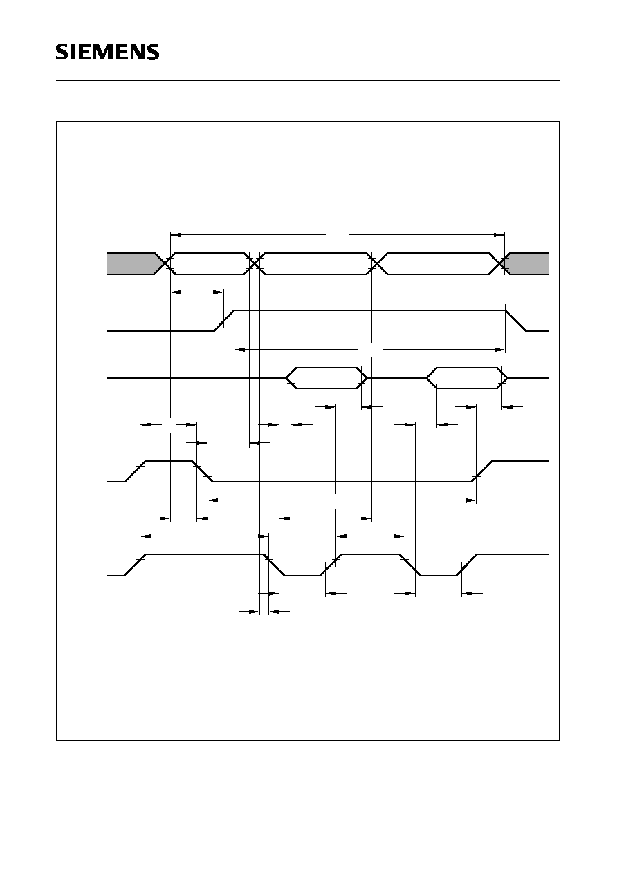
Output Timing: HS, VS, TCSQ
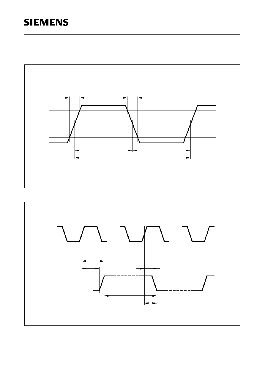
Hold and delay time with respect to 24-MHz system clock output:
Delay time
t
OD
20
ns
see diagram 2
Hold time
t
OH
0
ns
see diagram 2
Hold and delay time with respect to 24-MHz external system clock input:
Delay time
not specified
Hold time
not specified
Input Timing: HS, VS
No synchronous input mode specified!
Clock Input/Output (see diagram 1)
Clock Input
H-input voltage
V
IH
2.0
V
DDD
V
L-input voltage
V
IL
≠ 1.0
0.8
V
Input capacitance
C
I
7
pF
Input leakage current
I
l
10
µ
A
V
IH
= 5.5 V
Period
T
c
40
24-MHz clock
T
c
35
27-MHz clock
Transition time
t
CR
,
t
CL
3
ns
Symmetry ratio
t
CH
/t
C
0.43
0.57
Clock Output
H-output voltage
V
OH
2.4
V
DDD
V
≠
I
OH
= 0.2 mA
L-output voltage
V
OL
0
0.4
V
I
OL
= 1.6 mA
Load capacitance
C
L
50
pF
Period
T
C
41.7
ns
20.5-MHz crystal
Transition time
t
CR
,
t
CF
5
ns
Symmetry ratio
t
CH
/t
C
0.3
0.5
ns

SDA 5273 / 75
SDA 5273-2 / 75-2
Semiconductor Group
15
1997-09-01
Characteristics (cont'd)
For modes with external clock MEGATEXT may only be operated in freerun mode as sync master. HS may not
be used as an input in these cases.
The RGB-output voltage is proportional to
V
REF
.
T
A
= 0 to 70
∞
C
Parameter
Symbol
Limit Values
Unit
Test Condition
min.
typ.
max.
RGB-Outputs
V
REF
= 3 V
no resistive load
RGB-GND = 0 V
Pin capacitance
C
P
7
V
Output voltage range
0
2.2
V
RGB-amplitude
1.1
1.25
1.55
V
R83:
RGB-GAIN (4:0) = 1F
H
DC-offset voltage
0.7
0.8
1.0
V
R83:
RGB-LEVL (2:0) = 7
Clamp level
0
V
DAC-resolution
4
bit
Diff. non-linearity
≠ 0.5
0.5
LSB
R83:
RGB-GAIN (4:0) = 1F
H
RGB-LEVL (2:0) = 0
Int. non-linearity
≠ 0.5
0.5
LSB
Output tracking
≠ 0.5
0.5
LSB
Output resistance
R
O
270
3-dB bandwidth
10
MHz
C
L
= 50 pF
Bus Connection: SDA, SCL, I
2
CEN (see diagram 4)
Inputs: SDA, SCL
H-input voltage
V
IH
3.0
V
DDD
V
L-input voltage
V
IL
≠ 1.0
1.5
V
Input capacitance
C
I
7
pF
Input leakage current
I
L
10
µ
A
V
IH
= 5.5 V
V
DD
= 0 V ... 5.5 V
1
2
R
O
C
L
-----------------------

SDA 5273 / 75
SDA 5273-2 / 75-2
Semiconductor Group
16
1997-09-01
Characteristics (cont'd)
T
A
= 0 to 70
∞
C
Parameter
Symbol
Limit Values
Unit
Test Condition
min.
typ.
max.
Open Drain Outputs: SDA, SCL
L-output voltage
V
OL
0
0.4
V
I
OL
= 3 mA
Sink current
I
OL
10
mA
I
2
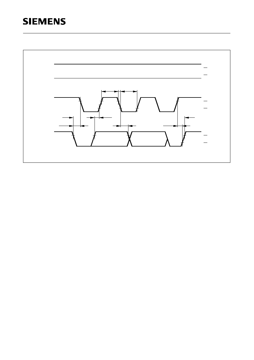
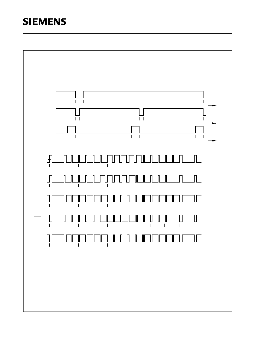
C-Mode Timing
MEGATEXT is an
I
2
C-slave transmitter/receiver.
The Siemens
I
2
C Bus specification applies.
SCL-frequency
f
SCL
0
100
kHz
I
2
CEN = high
Transition time
t
r
,
t
f
2
µ
s
Bus capacitance
C
BUS
400
pF
Bus free before start
t
BUF
4.7
µ
s
Hold time start
t
HSTA
4.0
µ
s
L-time clock
t
LOW
4.0
µ
s
H-time clock
t
HIGH
4.0
µ
s
Set-up time start
t
SUSTA
4.0
µ
s
Hold time SDA
t
HDDAT
0
µ
s
Set-up time SDA
t
SUDAT
250
ns
Set-up time SDA at stop
t
SUSTO
4.0
µ
s
Output fall time
t
FO
0.2
µ
s
3 V to 1 V
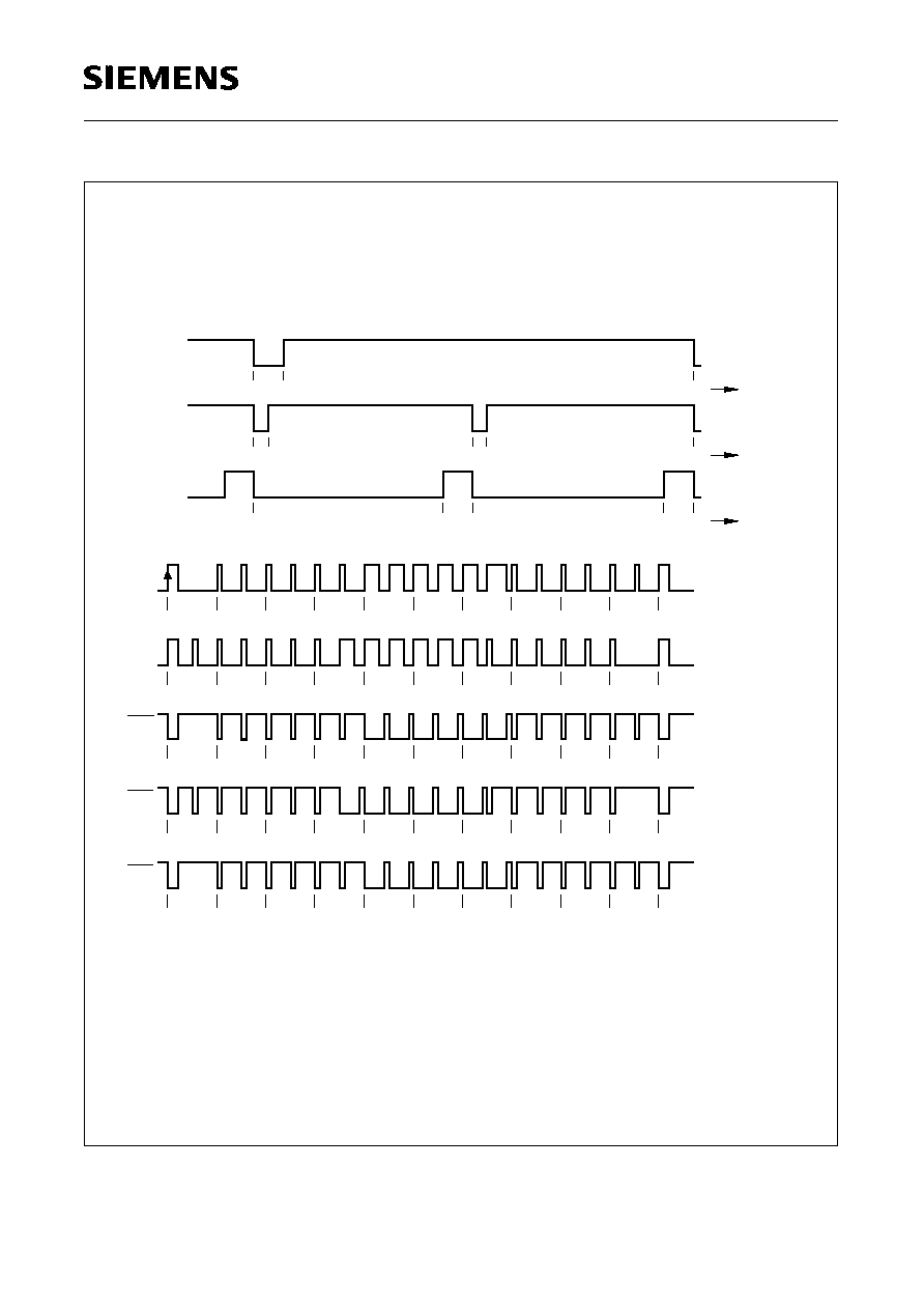
M3L-Mode Timing
The MEGATEXT M3L-Bus is specified in accordance with the standard USART-interface of micro
controller SDA 30C162.
SCL-frequency
f
SCL
0
1.0
MHz
20.48-MHz crystal
L-time clock
t
L
400
ns
H-time clock
t
H
400
ns
SCL-load capacitance
C
SCL
200
pF
Set-up time SDA-input to
SCL-falling edge
t
DSL
100
ns
Hold time SDA-input from
SCL-falling edge
t
DHH
400
ns

SDA 5273 / 75
SDA 5273-2 / 75-2
Semiconductor Group
17
1997-09-01
Characteristics (cont'd)
T
A
= 0 to 70
∞
C
Parameter
Symbol
Limit Values
Unit
Test Condition
min.
typ.
max.
M3L-Mode Timing (cont'd)
Set-up time SDA to I
2
CEN-
rising edge
t
IM
400
ns
Set up time I
2
CEN to SDA-
falling edge
t
IS
400
ns
I
2
CEN-high time
t
IH
1000
ns
Delay from SCL-falling edge
until SDA-open drain output
stage changes impedance
t
DO
400
600
ns
L-SDA level output
impedance
100
The resulting delay of SDA-output data is the sum of the open drain stage plus the time
determined by the bus capacitance and the external pullup resistor or the impedance of the
internal open drain pulldown transistor respectively.
Wait condition
I
2
CEN = 0
To force the M3L-master to interrupt the transmission sequence until MEGATEXT is ready for
more data, MEGATEXT can force down SCL after the transmission of a complete byte. At that
time the bus master has to switch its SCL-output to high impedance and check the state of SCL
afterwards.During SCL check
I
2
CEN has to be low.
Delay from SCL-rising edge
to SCL forced low for WAIT-
condition
t
DWAIT
500
750
ns
An internal pullup transistor restores SCL high level at the end of the WAIT-condition.
SCL-pullup time at the end of
WAIT
t
RWAIT
70
100
ns
Reference Voltage:
V
REF
Voltage level
V
REF
2.8
3.0
3.5
V
Input leakage current
I
l
≠ 10
10
µ
A
V
REF
= 3 V
V
REF
influences the DAC-range, the CVBS-output at pin TCSQ and the CVBS-ADC range.
SDA 5273 / 75
SDA 5273-2 / 75-2
Semiconductor Group
18
1997-09-01
Characteristics (cont'd)
The center frequency of the MEGATEXT horizontal PLL is proportional to the crystal frequency. In PAL-mode the
centre frequency is 15.625 kHz for the typical crystal frequency of 20.48 MHz. Deviations from the typical crystal
frequency will shift the range of the horizontal frequencies where the PLL is able to lock.
T
A
= 0 to 70
∞
C
Parameter
Symbol
Limit Values
Unit
Test Condition
min.
typ.
max.
CVBS-Input and ADC (
V
REF
= 3 V)
Input leakage current
I
l
≠ 1.0
1.0
µ
A
CVBS = 2 V
Input capacitance
C
P
45
pF
Ext. coupling capacitance
C
CPL
100
nF
Sensitivity of clamp level to
current leakage/injection
≠ 15
15
mV/
µ
A
I
l
= 2
µ
A
C
CPL
= 100 nF
ADC-range
1.7
2.0
V
V
REF
= 3 V
CVBS-sync amplitude
0.1
V
Crystal Oscillator: XIN, XOUT
Bias resistance between XIN,
XOUT
R
Xbias
60
120
180
k
Small signal voltage gain
G
V
8
13
100 kHz, 50 mVpp
Feedback capacitance
C
FB
4.0
pF
Pin capacitance
C
P
7.0
pF
Crystal
Nominal frequency
f
O
20.48
MHz
Effect of temperature and
accuracy of adjustment
d
f/f
O
≠ 5 %
+ 5 %
Temperature range
T
A
0
70
∞
C
Resonant impedance
Z
R
40
Equivalent parallel
C
C
L
15
pF
Crystal load
0.1
mW
Ext. capacitors
C
1,2
15
pF
SDA 5273 / 75
SDA 5273-2 / 75-2
Semiconductor Group
19
1997-09-01
Characteristics (cont'd)
T
A
= 0 to 70
∞
C
Parameter
Symbol
Limit Values
Unit
Test Condition
min.
typ.
max.
DRAM-Interface (see diagram 5)
The external DRAM is operated in page mode.
The timing of the DRAM-interface signals are specified below.
Cycle time
t
WC
420
500
550
ns
Address hold time from RAS
t
RAH
25
ns
Address hold time from CAS
t
CAH
60
ns
Address set-up time from
RAS
t
ASR
5
ns
Address set-up time from
CAS
t
ASC
5
ns
L-time RAS
t
RASP
280
ns
L-time CAS
t
CASL
70
ns
H-time RAS
t
RP
140
ns
H-time CAS
t
CP
70
ns
Refresh period
20
ms
Write Cycle
L-time WE
t
WEL
210
ns
Data set-up time to CAS
t
DS
100
ns
WE set-up time to CAS
t
RCS
0
ns
Data hold time from CAS
t
DH
55
ns
Data hold time from WE
t
OHZ
10
ns
Read Cycle
H-time WE (output enable)
t
OEL
210
ns
Access time from CAS
t
CAC
60
ns
Data hold time of DRAM
t
OFF
40
ns

SDA 5273 / 75
SDA 5273-2 / 75-2
Semiconductor Group
20
1997-09-01
Characteristics (cont'd)
T
A
= 0 to 70
∞
C
Parameter
Symbol
Limit Values
Unit
Test Condition
min.
typ.
max.
Reset/Chip Initialization
A power-on reset or a reset pulse at pin RES lead to a hardware reset and a software initialization
of registers and internal DRAM. During initialization bus transfers are not allowed.
At / after power-on a reset pulse at pin RES is necessary. RES may return to 0 after the supply
voltage reached its lower limit for chip function (4.7 V). This may be achieved by a capacitor
C
between RES and
V
DD
and by a resistor
R
between RES and
V
SS
. The dimensions of
R
and
C
depend on the worst case rise time of
V
DD
.
Initialization time after power-
on or falling edge of RES
t
INIT
25
ms
V
DD
greater 4.7 V
If the supply voltage drops below
V
DD min
, the IC has to be reset by pin RES.
Pulse width RES
100
ns
High level at pin RES causes chip reset.
In rare cases, the IC may remain in a permanent reset state after power up, depending on the
applicational context. After power up, the software should check proper operation. In case the
Megatext does not react properly, power supply should be switched off for at least 3 s. After that,
power supply can be switched on again.
Other Items
Horizontal frequency pull-in
range of CVBS-PLL:
15
15.625 16.2
kHz
PAL
20.48 MHz crystal
15.2
15.748 16.3
kHz
NTSC
20.48 MHz crystal
Horizontal frequency pull-in
range of display-PLL:
15
15.625 16.2
kHz
20.48 MHz crystal
SDA 5273 / 75
SDA 5273-2 / 75-2
Semiconductor Group
21
1997-09-01
3
Diagrams
Timing Diagram 1
Timing Diagram 2
UET04660
t
CR
t
CF
t
CH
t
CL
t
C
CLK
2.0 V
1.5 V
0.8 V
UET04662
OD
t
2.4 V
1.5 V
0.8 V
2.4 V
0.8 V
VS
HS
t
OH
OH
t
t
OD
W
t
CLK_OUT
SDA 5273 / 75
SDA 5273-2 / 75-2
Semiconductor Group
22
1997-09-01
Timing Diagram 3a
I
2
C-Bus Mode
UET04815
SCL
SDA
CEN
2
t
BUF
t
HIGH
t
LOW
f
t
V
IL
IH
V
V
IL
IH
V
V
IL
IH
V
BUF
t
t
SUSTA
SUDAT
t
t
HDDAT
SUSTO
t

SDA 5273 / 75
SDA 5273-2 / 75-2
Semiconductor Group
23
1997-09-01
Timing Diagram 3b
M3L-Bus Mode
UET04816
SCL
IS
t
SDA
CEN
2
SCL
Wait Condition
t
BUF
t
HIGH
t
LOW
f
t
t
r
t
IM
DS
t
DHH
t
t
DHH
DSL
t
t
DO
WAIT
t
DWAIT
RWAIT
t
V
IH
IL
V
V
OL
OL
V
V
IL
IH
V
V
IL
IH
V
V
IL
IH
V
BUF
t

SDA 5273 / 75
SDA 5273-2 / 75-2
Semiconductor Group
24
1997-09-01
Timing Diagram 4a
DRAM-Page Mode Write Cycle
Data from SDA 527x
Column Address
t
RASQ
CASQ
t
CP
ASR
t
ASC
t
t
CASL
D3
D0...
WEQ
A11
A0...
Row Address
t
RP
t
WE
t
RAH
DS
t
t
RASP
CAH
t
CP
CASL
t
UET04663
OHZ
Column Address
DH
t
WEL
t
WC
t
Data from SDA 527x
DS
t
t
DH
t
SDA 5273 / 75
SDA 5273-2 / 75-2
Semiconductor Group
25
1997-09-01
Timing Diagram 4b
DRAM-Page Mode Read Cycle
Data from RAM
Column Address
CAH
RAH
CASQ
RASQ
t
t
ASB
CP
ASC
t
t
CASL
t
WEQ
D3
D0...
A11
A0...
Row Address
t
RP
t
OE
t
t
CAC
t
RASP
t
CP
CASL
t
UET04664
Column Address
t
t
OFF
OEL
RC
t
Data from RAM
CAC
t
t
OFF
SDA 5273 / 75
SDA 5273-2 / 75-2
Semiconductor Group
26
1997-09-01
Timing Diagram 5a
VCS and TCS in PAL Freerun Mode
UED04865
a)
b)
c)
0
4.7
0 2.35
0
32 34.35
27.3
32
64
64
59.3
64
t [
µ
s]
]
s
µ
[
t
]
s
µ
[
t
622
623
624
625
1
2
3
4
5
6
310
311
312
313
314
315
316
317
318
319
(309)
(310)
(311)
(312)
1
2
3
4
5
6
(6)
(5)
(4)
(3)
(2)
(1)
309
310
311
312
1
2
3
4
5
6
(1)
(2)
(3)
(4)
(5)
(6)
(311)
(312)
(313)
(310)
(621)
(624)
(623)
(622)
(624)
(625)
(626)
(623)
VCS
VCS
TCS
TCS
TCS
Interlaced
Interlaced
Non-
Interlaced
-312/312 Lines
-313/312 Lines
-626/624 Lines
Main Pulse
Equalizing Pulse
Line Sync Pulse
Timing with Tolerances 100 ns
(312)
(311)
(310)
(309)
6
5
4
3
2
1
625
624
623
622
319
318
317
316
315
314
313
312
311
310
±
SDA 5273 / 75
SDA 5273-2 / 75-2
Semiconductor Group
27
1997-09-01
Timing Diagram 5b
VCS and TCS in NTSC Freerun Mode
Interlaced
Interlaced
Non-
Interlaced
-262/262 Lines
-263/262 Lines
-526/524 Lines
TCS
TCS
TCS
VCS
VCS
0
4.7
63.6
63.6
31.8
27.1
0
34.1
2.3
63.6
0
Main Pulse
Equalizing Pulse
Line Sync Pulse
UED04872
58.9
31.8
522
(259)
523
(260)
524
(261)
525
(262)
1
2
3
4
5
6
t [ s]
t [ s]
t [ s]
260
261
262
263
264
(1)
265
(2)
266
(3)
267
(4)
268
(5)
269
(6)
259
(260)
(521)
(523)
260
(261)
(522)
(524)
261
(262)
(523)
(525)
262
(263)
(524)
(526)
1
(1)
2
(2)
3
(3)
4
(4)
5
(5)
6
(6)
522
(259)
523
(260)
524
(261)
525
(262)
1
2
3
4
5
6
260
261
262
263
264
(1)
265
(2)
266
(3)
267
(4)
268
(5)
269
(6)
a)
b)
c)
µ
µ
µ

SDA 5273 / 75
SDA 5273-2 / 75-2
Semiconductor Group
28
1997-09-01
Application Circuit
UES04659
RASQ
WEQ
10
11
12
13
14
15
16
17
18
19
20
21
22
23
24
25
26
CVBS
44
45
46
47
48
49
50
51
52
53
54
55
56
57
58
59
60
GPO
XOUT
VS
SDA
SCL
CORQ
BLAN
B
V
RESET
G
V
2
CEN
V
V
SS1
SSA2
SS4
27
28
29
30
31
32
33
34
35
36
37
38
39
40
41
42
43
9
8
7
6
5
4
3
2
1
68
67
66
65
64
63
62
61
SDA 527x
10
nF
220
V
DD
ZD
V
3
220 nF
nF
100
DD
V
V
SS
4.7
k
150
150
k
4.7
V
DD
Blank
Reduction
DD
V
22 pF
HS
HS
INTQ
SCL G B
TTL
VS
TTL
CVBS
CEN
2
270
1.15 Vpp
V
DD
10
µ
F
470
Ref.
V
5
2 Vpp
20.48 MHz
XIN
TM
TCSQ
CLK
INTQ
R
TCSQ
TTL
R
SDA
Contrast
k
100
RGB-GND
BB
V
SS2
V
N.C.
N.C.
N.C.
N.C.
N.C.
N.C.
N.C.
N.C.
N.C.
CASQ
DRAM
A1
A0
A9
A10
A11
D1
D0
D2
D3
A2
A3
A4
A5
A6
A7
DD4
V
DD1
V
DDA
V
SSA1
V
DD2
V
DD3
V
REF
N.C.
N.C.
N.C.
N.C.
N.C.
N.C.
N.C.
A8
k
220
F
n
SS3
V
22 pF

SDA 5273 / 75
SDA 5273-2 / 75-2
Semiconductor Group
29
1997-09-01
4
Package Outlines
GPL05099
0.81 max
1.27
0.43 ±0.1
0.18
M
68x
D
A-B
20.32
0.1
5.08 max
3.5 ±0.2
0.5 min
0.2
1.2 x 45∞
23.3 ±0.3
24.21 ±0.07
25.28 -0.26
1)
0.38
M
D
A-B
34x
A
B
D
1
68
0.5 x 45∞
3 x
24.21 ±0.07
1)
25.28 -0.26
1.1 x 45∞
Index Marking
1) Does not include plastic or metal protrusions of 0.15 max per side
P-LCC-68-1 (SMD)
(Plastic Leaded Chip Carrier)
Sorts of Packing
Package outlines for tubes, trays etc. are contained in our
Data Book "Package Information".
Dimensions in mm
SMD = Surface Mounted Device

SDA 5273 / 75
SDA 5273-2 / 75-2
Semiconductor Group
30
1997-09-01
46.1
0.25
14.02
15.24
1.78
0.46
52
27
1
26
1.3 max
0.5 min
3.43
4.83 max
-0.3
±0.25
-0.4
±0.05
±0.1
0.25 max
+1.7
Index Marking
+0.7
15.24
M
0.25
52x
Plastic Package, P-SDIP-52-1
(Plastic Dual In-Line Package)
GPD05262
Sorts of Packing
Package outlines for tubes, trays etc. are contained in our
Data Book "Package Information".
Dimensions in mm
SMD = Surface Mounted Device