
Type
Ordering Code
Package
SDA 9251-2X
Q67100-H5063
P-DSO-28-.350 (SMD)
868352-Bit Dynamic Sequential Access Memory
for Television Applications (TV-SAM)
Preliminary Data
CMOS IC
SDA 9251-2X
P-DSO-28-.350
Features
q
212 x 64 x 16 x 4-bit organization
q
Triple port architecture
q
One 16 x 4-bit input shift register
q
Two 16 x 4-bit output shift registers
q
Shift registers independently and simultaneously
accessible
q
Continuous data flow even at maximum speed
q
33-MHz shift rate - 0.27-Gbit/s total data rate
q
All inputs and outputs TTL-compatible
q
Tristate outputs
q
Random access of groups of 16 x 4 bits for a wide range
of applications
q
Refresh-free operation possible
q
5 V
±
10 % power supply
q
0 ... 70
∞
C operating temperature range
q
Low power dissipation: 550 mW active, 28 mW standby
q
Suitable for all common TV standards
q
Allows flicker and noise reduction simultaneously
with only one field memory
q
Applications: TV, VCR, image processing,
video printers, data compressors, delay lines,
time base correctors, HDTV
Semiconductor Group
159
01.94

SDA 9251-2X
Semiconductor Group
160
Functional Description
The SDA 9251 is a triple port 868 352 bit dynamic sequential-access memory for high-data-rate
video applications. It is organized as 212 rows by 64 columns by 16 arrays by 4 bit to allow for the
storage of 4-bit planes of a TV field (NTSC, PAL, SECAM, MAC) in standard or studio quality
(13.5-MHz basic sample rate) or 4-bit planes of parts of a HDTV field. The memory is fabricated
using the same CMOS technology used for 1-Mbit standard dynamic random access memories.
The extremely high maximum data rate is achieved by three internal shift registers, each of 16-bit
length and 4-bit width, which perform a serial to parallel conversion between the asynchronous
input/output data streams and the memory array. The parallel data transfer from the 16 x 4-bit input
shift register C to an addressed location of the memory array and from the memory array to one of
the 16 x 4-bit output shift registers A or B is controlled by the serial column address (SAC) which
contains the desired column address and an instruction code (mode bits) for transfer and refresh.
Circuit Description
Memory Architecture
As shown in the block diagram, the TV-SAM comprises 64 memory arrays which are accessed in
parallel. Each memory array has a size of 212 rows by 64 columns. The rows and columns of the
64 (= 16 x 4) arrays can be randomly addressed, reading or writing 16 x 4 bits at a time. To obtain
the extremely high data rate at the 4-bit wide data input (SDC) and outputs (SQA, SQB), a parallel
to serial conversion is done using shift registers of 16-bit length and 4-bit width. In this way the
memory speed is increased by a factor of 16. (This is independent on the number of ports if the total
data rate is regarded.)
Independent operation of the serial input and the two serial outputs is guaranteed by using three
shift registers. The decoupling from the common 16 x 4-bit memory data bus is done by three
latches which allow a flexible memory timing and a flying real-time data transfer.
A real-time data transfer is necessary to ensure a continuous data flow at the data pins even at
maximum clock speed.
To save pins without loosing speed, the TV-SAM is addressed serially using a serial 8-bit row
address and a serial 8-bit column address which includes two mode control bits. The serial row and
column addresses are converted to parallel addresses internally, then latched and fed to the row
and column decoders. The internal memory controller is responsible for the timing of the memory
read/write access and the refresh operation.

SDA 9251-2X
Semiconductor Group
161
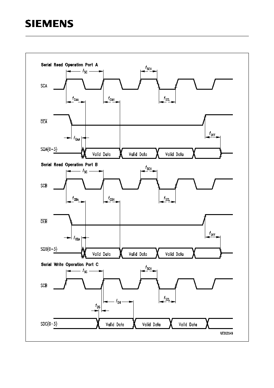
Data Input (SDC, SCB)
Data are shifted in through the serial port C (SDC0, ..., SDC3) at the rising edge of the shift clock
SCB. After16 clock pulses the data have to be transferred from shift register C to latch C. If more
than 16 clock pulses occur before latching the data, only the last sixteen 4-bit data values are
accepted.
Data Transfer from Shift Register C to Latch C (WT)
The contents of the shift register C are transferred to latch C at the falling edge of the write transfer
signal WT. If the timing restrictions between WT and the clock SCB are respected, a continuous
data flow at input SDC is possible without loosing data. This transfer operation may be
asynchronous to all other transfer operations except for a small forbidden window conditioned by
the latch C to memory transfer, see diagram 4.
Write Transfer from Latch C to Memory (RE)
The data of latch C are transferred to the preaddressed location of the memory array at the rising
edge of RE, if the mode bits were set to H (M1) and L (M0), see "Addressing and Mode Control."
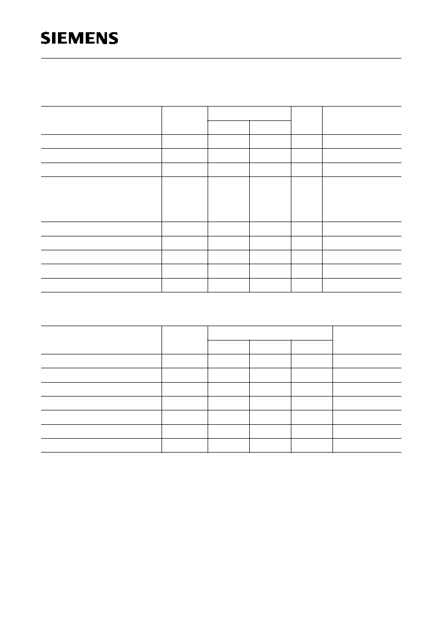
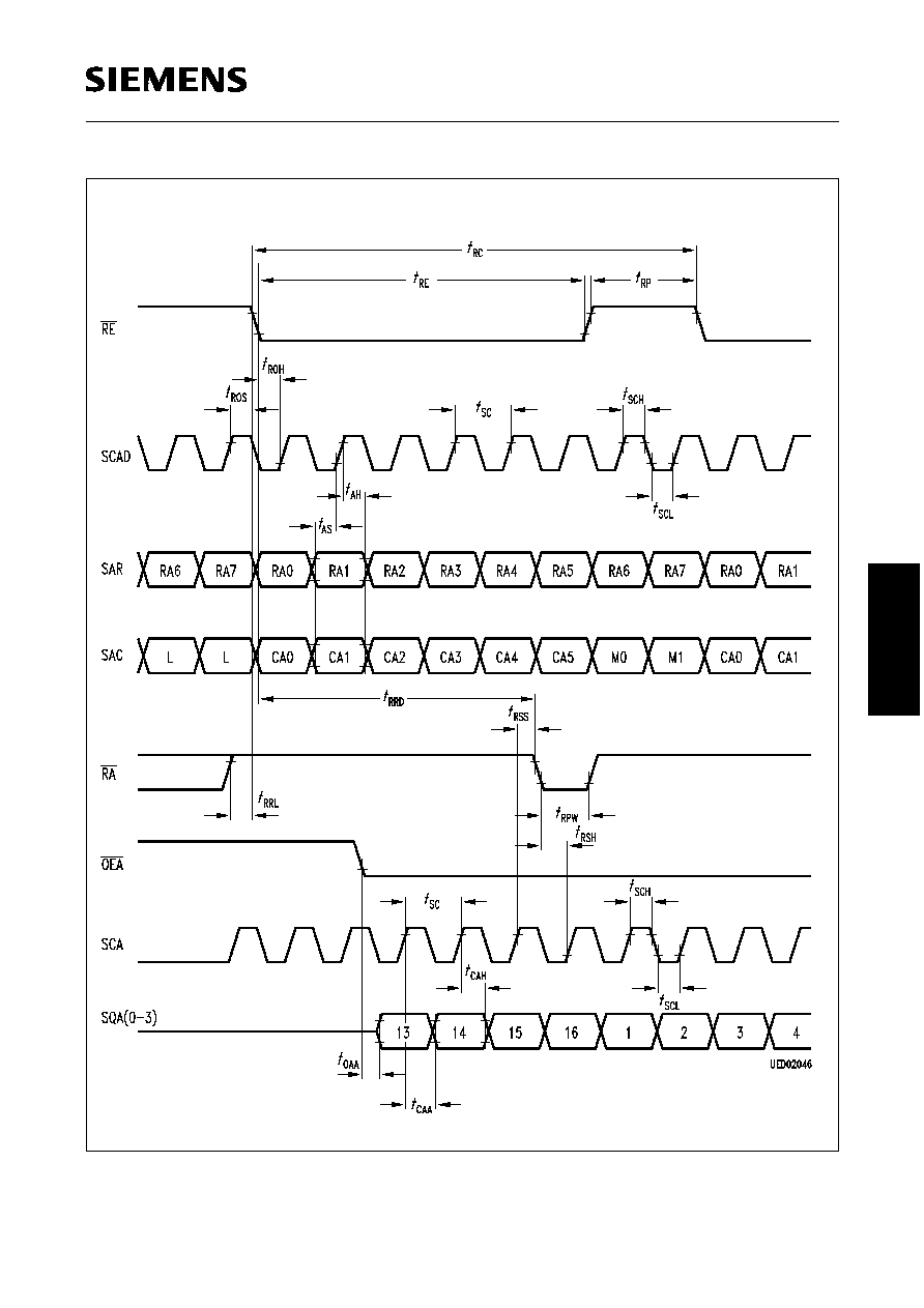
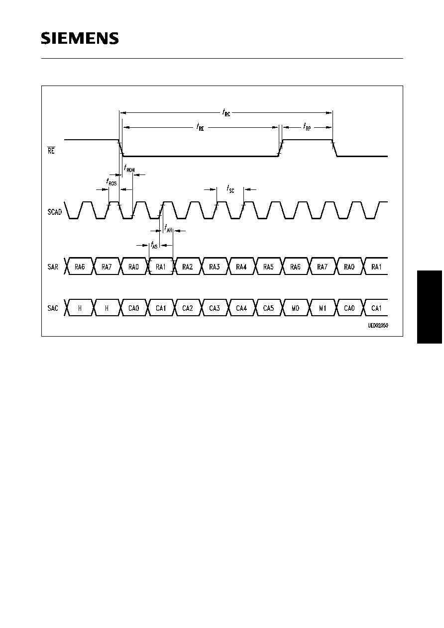
Addressing and Mode Control (SAR, SAC, SCAD, RE)
The serial 8-bit row address SAR and the 8-bit column address/mode code SAC are serially shifted
into the TV-SAM (LSB first) at rising edge of the address clock SCAD. After 8 SCAD cycles, the
falling edge of RE internally latches SAR and SAC. The column address itself needs only 6 bits. The
last 2 bits of SAC are defined as mode bits and determine the read/write and refresh operation of
the memory arrays to be triggered by the RE signal.
Read Transfer from Memory to Latch A or B (RE)
Memory data from a preaddressed location are transferred to latch A or B at the falling edge of RE,
depending on the mode control bits, see "Addressing and Mode Control".
Data Transfer from Latch A to Shift Register A (RA)
The contents of latch A are transferred to shift register A at the falling edge of the read transfer
signal RA. If the timing restrictions between RA and the shift clock SCA are taken into account, a
continuous data flow at output SQA without interrupts is possible. This transfer operation is
independent on all other transfer operations except for a small forbidden time window conditioned
by the memory to latch A transfer.
Mode Bit M1
Mode Bit M0
Operation
L
L
Read transfer from memory to latch A
L
H
Read transfer from memory to latch B
H
L
Write transfer from latch C to memory
H
H
Refresh with internal row address

SDA 9251-2X
Semiconductor Group
162
Data Transfer from Latch B to Shift Register B (RB)
The contents of latch B are transferred to shift register B at the falling edge of the read transfer
signal RB. If the timing restrictions between RB and the shift clock SCB are taken into account, a
continuous data flow at output SQB without interrupts is possible. This transfer operation is
independent on all other transfer operations except for a small forbidden time window conditioned
by the memory to latch B transfer.
Data Output A (SQA, SCA, OEA)
Data is shifted out through the serial port A (SQA0 ... SQA3) at the rising edge of the shift clock
SCA. After 16 clock cycles new data have to be transferred from latch A to shift register A.
Otherwise data values are cyclically repeated.
Via the output enable OEA the output buffers can be switched into tristate.
The shift clock SCA may be completely independent on the shift clock for port B and C (SCB).
Data Output B (SQB, SCB, OEB)
Data is shifted out through the serial port B (SQB0 ... SQB3) at the rising edge of the shift clock
SCB. After 16 clock cycles new data have to be transferred from latch B to shift register B.
Otherwise data values are cyclically repeated. The shift clock SCB is also used for the input port C.
Via the output enable OEB the output buffers can be switched into tristate.
Refresh
Either 256 refresh cycles or read/write cycles on 212 consecutive row addresses have to be
executed within an 8 ms interval to maintain the data in the memory arrays.
A refresh cycle is determined by the mode control bits, see "Addressing and Mode Control". In the
refresh mode, the row and column addresses are ignored.
It should be noted that the shift registers are also dynamic storage elements and that the data will
be lost unless shifted using clocks SCA, SCB and SCAD within the specified retention time.
Initialization
The device incorporates an on-chip substrate bias generator as well as dynamic circuitry. Therefore
an initial pause of 200
µ
s is required after power on, followed by eight RE-cycles before proper
device operation is achieved.

SDA 9251-2X
Semiconductor Group
163
Typical Memory Cycle Sequence
A typical application of the TV-SAM is a real-time interfield image processing combined with flicker
reduction. This can be achieved, for example, by writing and reading with 13.5-MHz clock rate via
port C and B and by simultaneously reading port A with 27-MHz double speed clock. A main cycle
of 4 consecutive RE cycles of transfer is needed:
1st.
RE-cycle:
Read transfer from memory to latch A
2nd.
RE-cycle:
Read transfer from memory to latch B
3rd.
RE-cycle:
Same as 1st. RE cycle
4th.
RE-cycle:
Write transfer from latch C to memory
Each transfer cycle is preceeded by an address cycle as shown in the diagram page 164:
For the clock rates mentioned this means a serial cycle time of 74 ns at port B and C and 37 ns at
port A. The addressing cycle time for each port is given by 16 times the serial data rate. Thus we
have an addressing cycle time of approx. 1184 ns for port B and port C. The address for port A must
be loaded every 592 ns. Since all addresses are shifted in sequentially, a RE cycle time of approx.
296 ns is necessary.
The beginning of a block of 16 serial data at port A or B is determined by RA and RB, respectively.
The end of the serial input data block at port C is controlled by WT. Since RA, RB and WT can be
independently chosen (except for small forbidden time windows when memory transfers are
executed), the serial data streams can be shifted against each other without influencing the RE
cycles.

SDA 9251-2X
Semiconductor Group
164
Typical Memory Cycle Sequence

SDA 9251-2X
Semiconductor Group
165
Pin Configuration
(top view)

SDA 9251-2X
Semiconductor Group
166
Pin Definitions and Functions
Pin No.
Symbol
Input (I)
Output (O)
Function
3
2
27
26
SQA0
SQA1
SQA2
SQA3
O
O
O
O
Serial data output for port A
20
SCA
I
Serial clock input for port A
19
RA
I
Read transfer control input (latch A to shift register A)
25
OEA
I
Output enable input for port A
5
4
24
23
SQB0
SQB1
SQB2
SQB3
O
O
O
O
Serial data output for port B
18
SCB
I
Serial clock input for port B and C
17
RB
I
Read transfer control input (latch B to shift register B)
22
OEB
I
Output enable input for port B
6
7
8
9
SDC0
SDC1
SDC2
SDC3
I
I
I
I
Serial data input for port C
16
WT
I
Write transfer control input (shift register C to latch C)
12
SAR
I
Serial row address input
13
SAC
I
Serial column address and mode control input
11
SCAD
I
Serial address clock input
10
RE
I
RAM-enable input (also latches the addresses)
1
V
CC1
Data output power supply (+ 5 V)
28
V
SS1
Data output power supply (GND)
14
V
CC2
Memory power supply (+ 5 V)
15
V
SS2
Memory power supply (GND)
21
(TF)
Test function (for factory use only)

SDA 9251-2X
Semiconductor Group
167
Block Diagram
SDA 9251-2X
Semiconductor Group
168
Absolute Maximum Ratings
Parameter
Symbol
Limit Values
Unit
Remarks
min.
max.
Storage temperature
T
stg
≠ 55
125
∞
C
Soldering temperature
T
sold
260
∞
C
Soldering time
t
sold
10
s
Input/output voltage
V
I/Q
≠ 1
7
V
Exception:
pin 21 = TF
≠ 1 to + 11 V
Test function input voltage
V
I
≠ 1
11
V
For factory use only
Power supply voltage
V
CC
≠ 1
7
V
Data out current (short circuit)
I
Q
25
mA
Total power dissipation
P
tot
900
mW
Power dissipation per output
P
Q
112
mW
Operating Range
Parameter
Symbol
Limit Values
Unit
min.
typ.
max.
Supply voltage
V
CC1
4.5
5.0
5.5
V
Supply voltage
V
CC2
4.5
5.0
5.5
V
Supply voltage
V
SS1
0
V
Supply voltage
V
SS2
0
V
H-input voltage
V
IH
2.4
6.5
V
L-input voltage
V
IL
≠ 1.0
0.8
V
Ambient temperature
T
A
0
25
70
∞
C

SDA 9251-2X
Semiconductor Group
169
DC Characteristics
V
CC
= 5 V
±
10 %;
T
A
= 0 to 70
∞
C
Parameter
Symbol
Limit Values
Unit
Test Condition
min.
typ.
max.
Test enable input
high voltage
V
IH
(TF)
V
CC
+
4.5
10.5
V
At normal operation the
pin TF has to be
connected to
V
IL
(TF) level
or left unconnected.
Test disable input
low voltage
V
IL
(TF)
≠ 1.0
V
CC
+
1.0
V
See test enable input high
voltage
H-output voltage
V
QH
2.4
V
I
OUT
= ≠ 2.5 mA
L-output voltage
V
QL
0.4
V
I
OUT
= 2.1 mA
Input leakage current
I
I (L)
≠ 10
10
µ
A
0 V
V
I
6.5 V
Output leakage current
I
Q (L)
≠ 10
10
µ
A
OEA = OEB =
V
IH
Average supply current
I
CCa
100
mA
(
t
SC
port A =
t
SC
min)
(
t
SC
port B = 2
t
SC
min)
(
t
SC
port C = 2
t
SC
min)
(
t
RC
=
t
RC
min)
I
CCa
depends on cycle rate
and on output loading.
Specified values are
measured with open
output.
Standby supply current
I
CCb
5
mA
(RE = OEA = OEB =
V
CC
)
t
SC
(SCA, SCB, SCAD) =
max. (
t
SC
)

SDA 9251-2X
Semiconductor Group
170
AC Characteristics
V
CC
= 5 V
±
10 %;
T
A
= 0 to 70
∞
C
Parameter
Symbol
Limit Values
Unit
Test Condition
min.
typ.
max.
Memory read or
write cycle time
t
RC
240
100000 ns
Operation with
t
RC
t
RCmin
ensures that 8-bit serial
data are shifted out within
one RE cycle taking
t
SC
=
t
SCmin
.
See diagram 2, 3, 4, 6
RE low time
t
RE
100
100000 ns
See diagram 2, 3, 4, 6
Serial port cycle
time
t
SC
30
100000 ns
See diagram 2 ≠ 6
RE precharge time
t
RP
100
ns
See diagram 2, 3, 4, 6
Address setup time
t
AS
5
ns
See diagram 2, 3, 4, 6
Address hold time
t
AH
6
ns
See diagram 2, 3, 4, 6
SCAD to RE
set-up time
t
ROS
3
ns
See diagram 2, 3, 4, 6
RE to SCAD
hold time
t
ROH
10
ns
See diagram 2, 3, 4, 6
RE to RA or RB
delay time
t
RRD
90
ns
t
RRD
and
t
RRL
are restrictive
operating parameters only
in memory read transfer
cycles.
See diagram 2, 3
RA or RB to RE
lead time
t
RRL
≠ 30
ns
See RE to RA or RB delay
time.
See diagram 2, 3
RA to SCA
RB to SCB
set-up time
t
RSS
0
ns
See diagram 2, 3
RA or RB
pulse width
t
RPW
10
ns
See diagram 2, 3
RA to SCA
RB to SCB
hold time
t
RSH
15
ns
See diagram 2, 3

SDA 9251-2X
Semiconductor Group
171
WT to RE lead time
t
WRL
30
ns
t
WRL
and
t
WRL
are restrictive
operating parameters only
in memory write transfer
cycles. In that case
t
WRL
applies if the write transfer
from shifter C to latch C
occurs before the rising
edge of RE. Otherwise
t
RWL
has to be satisfied.
See diagram 4
RE to WT lead time
t
WRL
50
ns
See WT to RE lead time
Output buffer turn-
off delay
t
OFF
0
20
ns
t
OFF
(max) defines the time
at which the output
achieves the open-circuit
condition and is not
referenced to output
voltages levels.
WT to SCB delay
time
t
WTD
0
ns
See diagram 4
WT to SCB lead
time
t
WTL
15
ns
See diagram 4
WT pulse width
t
WTP
10
ns
See diagram 4
OEA to output A
access time
t
OAA
25
ns
See diagram 2, 5
OEB to output B
access time
t
OBA
25
ns
See diagram 3, 5
Access time from
SCA
t
CAA
25
ns
See diagram 2
Access time from
SCB
t
CBA
25
ns
See diagram 3
Data input set-up
time to SCB
t
DS
5
ns
See diagram 5
Data input hold time
to SCB
t
DH
6
ns
See diagram 5
AC Characteristics (cont'd)
V
CC
= 5 V
±
10 %;
T
A
= 0 to 70
∞
C
Parameter
Symbol
Limit Values
Unit
Test Condition
min.
typ.
max.

SDA 9251-2X
Semiconductor Group
172
Refresh period
t
REF
8
ms
Either 256 refresh cycles
or read/write cycles on 212
consecutive row
addresses have to be
performed within the 8 ms
interval to maintain data
Transition time
(rise/fall)
t
T
2
10
ns
Transition times are
measured between
V
IH
and
V
IL
.
See diagram 1
L-serial clock time
t
SCL
10
ns
See diagram 2
H-serial clock time
t
SCH
10
ns
See diagram 2
Hold time from SCA
t
CAH
6
ns
See diagram 2
Hold time from SCB
t
CBH
6
ns
See diagram 3
Input capacitance
(SCA, SCB)
C
I 1
7
pF
f
= 1 MHz
Input capacitance
(all other pins)
C
I 2
5
pF
f
= 1 MHz
Output capacitance
(SQA 0-3, SQB 0-3)
C
Q
7
pF
f
= 1 MHz
AC Characteristics (cont'd)
V
CC
= 5 V
±
10 %;
T
A
= 0 to 70
∞
C
Parameter
Symbol
Limit Values
Unit
Test Condition
min.
typ.
max.

SDA 9251-2X
Semiconductor Group
173
Operation Truth Table
RE Cycle
N
RE Cycle
N
+ n, n = 1, 2, 3 ...
SCAD
SAR
SAC
Mode
OEA
OEB
SCA
SCB
RA
RB
WT
Operation
M0
M1
RA0...RA7 CA0...CA5
L
L
X
X
X
X
X
X
Read transfer from
memory to shifter A
RA0...RA7 CA0...CA5
H
L
X
X
X
X
X
X
Read transfer from
memory to shifter B
RA0...RA7 CA0...CA5
L
H
X
X
X
X
X
X
Write transfer from
shifter C to memory
X
X
H
H
X
X
X
X
X
X
X
Refresh with
internal row address
X
X
X
X
X
L
X
X
X
X
X
Serial read port A
X
X
X
X
X
X
L
X
X
X
X
Serial read port B
X
X
X
X
X
X
X
X
X
X
X
Serial read port C
Note: X = Dont't care
V
(TF) =
V
IL
(TF) or not connected
Row address, column address and mode bits have to be
defined in RE cycle
N
in order to become effective in RE
cycle
N
+ 1

SDA 9251-2X
Semiconductor Group
174
Diagram 1
AC-Timing Measuring Conditions
SDA 9251-2X
Semiconductor Group
175
Diagram 2
Read Transfer Memory to Port A
SDA 9251-2X
Semiconductor Group
176
Diagram 3
Read Transfer Memory to Port B

SDA 9251-2X
Semiconductor Group
177
Diagram 4
Write Transfer from Port C to Memory
SDA 9251-2X
Semiconductor Group
178
Diagram 5
SDA 9251-2X
Semiconductor Group
179
Diagram 6
Refresh with Internal Row Address

SDA 9251-2X
Semiconductor Group
180
Application Circuit
For best performance and operation within the specified AC parameter limits it is mandatory to use
separate decoupling capacitors for
V
SS1
/
V
CC1
and
V
SS2
/
V
CC2
with
V
SS1
shorted to
V
SS2
and
V
CC1
shorted to
V
CC2
on the board as shown in figure below.
Decoupling capacitors
C
1
and
C
2
of low inductance multilayer type (at least 0.1
µ
F) should be used.
To avoid malfunction or even permanent damage of the device it is strongly recommended not to
use any other supply configuration.

SDA 9251-2X
Semiconductor Group
181
Typical Application
Digital Storage of a TV Field
As standard for digital TV systems, CCIR recommendation 601 defines a field of 288 lines with 720
pixels per line.
The sampling frequency is 13.5 MHz with a resolution of 8 bit per pixel.
Information is stored in 3 different channels: one channel for luminance (Y), two channels for
chrominance (U and V).
The bandwidth ratio between the different channels is either Y:U:V = 4:1:1, 4:2:2 or 4:4:4 depending
on the coding method.
HDTV will have a sampling frequency of 54 MHz.
The following tables show the memory requirements for the field buffer and the number of memory
chips when the SDA 9251 is used.
Table 1
Memory Requirements for the Digital TV-Field Buffer
Table 2
Number of Required Memory Devices in the Field Buffer when Using the SDA 9251
Clock Rate
Bus Width
Y:U:V
13.5 MHz
54 MHz
4:1:1
4:2:2
4:4:4
2.37 Mbit
3.16 Mbit
4.75 Mbit
9.49 Mbit
12.66 Mbit
18.98 Mbit
12 bit
16 bit
24 bit
Clock Rate
Bus Width
Y:U:V
13.5 MHz
54 MHz
4:1:1
4:2:2
4:4:4
3
4
6
12
16
24
12 bit
16 bit
24 bit