 | –≠–ª–µ–∫—Ç—Ä–æ–Ω–Ω—ã–π –∫–æ–º–ø–æ–Ω–µ–Ω—Ç: SDA9270 | –°–∫–∞—á–∞—Ç—å:  PDF PDF  ZIP ZIP |

ICs for Consumer Electronics
Field Mixer
SDA 9270
Data Sheet 01.96
Edition 01.96
This edition was realized using the software system FrameMaker
Æ
.
Published by Siemens AG,
Bereich Halbleiter, Marketing-
Kommunikation, Balanstraþe 73,
81541 M¸nchen
©
Siemens AG 1996.
All Rights Reserved.
Attention please!
As far as patents or other rights of third parties are concerned, liability is only assumed for components, not for applications, processes
and circuits implemented within components or assemblies.
The information describes the type of component and shall not be considered as assured characteristics.
Terms of delivery and rights to change design reserved.
For questions on technology, delivery and prices please contact the Semiconductor Group Offices in Germany or the Siemens Companies
and Representatives worldwide (see address list).
Due to technical requirements components may contain dangerous substances. For information on the types in question please contact
your nearest Siemens Office, Semiconductor Group.
Siemens AG is an approved CECC manufacturer.
Packing
Please use the recycling operators known to you. We can also help you ≠ get in touch with your nearest sales office. By agreement we
will take packing material back, if it is sorted. You must bear the costs of transport.
For packing material that is returned to us unsorted or which we are not obliged to accept, we shall have to invoice you for any costs in-
curred.
Components used in life-support devices or systems must be expressly authorized for such purpose!
Critical components
1
of the Semiconductor Group of Siemens AG, may only be used in life-support devices or systems
2
with the express
written approval of the Semiconductor Group of Siemens AG.
1 A critical component is a component used in a life-support device or system whose failure can reasonably be expected to cause the
failure of that life-support device or system, or to affect its safety or effectiveness of that device or system.
2 Life support devices or systems are intended (a) to be implanted in the human body, or (b) to support and/or maintain and sustain hu-
man life. If they fail, it is reasonable to assume that the health of the user may be endangered.
SDA 9270
Revision History:
Current Version: 01.96
Previous Version:
Page
Subjects (changes since last revision)
24
HYTHL1 control bits have been increased to 6
25
HYTHL2 control bits have been increased to 6
25
HYTHH1 control bits have been increased to 6
25
HYTHH2 control bits have been increased to 6
27
Clock inputs CLL, SCA, SCAD:
SCA clock frequence MIN changed to 12 MHz
SCAD clock specification added
Fall/rise time specification added
27
I
2
C-Bus specification extended to fast mode
29
Max. average supply current: 200 mA

General Information
Table of Contents
Page
Semiconductor Group
3
1
Introduction . . . . . . . . . . . . . . . . . . . . . . . . . . . . . . . . . . . . . . . . . . . . . . . . . 4
1.1
Features . . . . . . . . . . . . . . . . . . . . . . . . . . . . . . . . . . . . . . . . . . . . . . . . . . . . . 4
1.2
Block Diagram . . . . . . . . . . . . . . . . . . . . . . . . . . . . . . . . . . . . . . . . . . . . . . . . 5
1.3
Pin Configuration . . . . . . . . . . . . . . . . . . . . . . . . . . . . . . . . . . . . . . . . . . . . . . 6
1.4
Pin Description . . . . . . . . . . . . . . . . . . . . . . . . . . . . . . . . . . . . . . . . . . . . . . . . 7
2
System Description . . . . . . . . . . . . . . . . . . . . . . . . . . . . . . . . . . . . . . . . . . . 8
2.1
Input Data Format . . . . . . . . . . . . . . . . . . . . . . . . . . . . . . . . . . . . . . . . . . . . . 9
2.2
Output Data Format . . . . . . . . . . . . . . . . . . . . . . . . . . . . . . . . . . . . . . . . . . . 10
2.3
Field Interpolation and Switching . . . . . . . . . . . . . . . . . . . . . . . . . . . . . . . . . 11
2.4
Motion Detection . . . . . . . . . . . . . . . . . . . . . . . . . . . . . . . . . . . . . . . . . . . . . 11
2.5
Field Memory Control . . . . . . . . . . . . . . . . . . . . . . . . . . . . . . . . . . . . . . . . . . 11
2.6
Frame Synchronization . . . . . . . . . . . . . . . . . . . . . . . . . . . . . . . . . . . . . . . . 11
2.7
SYNC-Signal Generation . . . . . . . . . . . . . . . . . . . . . . . . . . . . . . . . . . . . . . . 12
2.8
I
2
C-Bus . . . . . . . . . . . . . . . . . . . . . . . . . . . . . . . . . . . . . . . . . . . . . . . . . . . . . 12
2.8.1
I
2
C-Bus Address . . . . . . . . . . . . . . . . . . . . . . . . . . . . . . . . . . . . . . . . . . . . . . 12
2.8.2
I
2
C-Bus Format . . . . . . . . . . . . . . . . . . . . . . . . . . . . . . . . . . . . . . . . . . . . . . 12
2.8.3
I
2
C-Bus Commands . . . . . . . . . . . . . . . . . . . . . . . . . . . . . . . . . . . . . . . . . . . 14
2.8.4
Detailed Description . . . . . . . . . . . . . . . . . . . . . . . . . . . . . . . . . . . . . . . . . . . 16
3
Electrical Characteristics . . . . . . . . . . . . . . . . . . . . . . . . . . . . . . . . . . . . . 25
3.1
Absolute Maximum Ratings . . . . . . . . . . . . . . . . . . . . . . . . . . . . . . . . . . . . . 25
3.2
Recommended Operating Conditions . . . . . . . . . . . . . . . . . . . . . . . . . . . . . 26
3.3
Characteristics (Assuming Recommended Operating Conditions) . . . . . . . 28
4
Application Information . . . . . . . . . . . . . . . . . . . . . . . . . . . . . . . . . . . . . . . 30
5
Waveforms . . . . . . . . . . . . . . . . . . . . . . . . . . . . . . . . . . . . . . . . . . . . . . . . . 31
6
Package Outlines . . . . . . . . . . . . . . . . . . . . . . . . . . . . . . . . . . . . . . . . . . . . 32
P-MQFP-80-1
Semiconductor Group
4
01.96
Field Mixer
SDA 9270
Preliminary Data
CMOS
∑
I
2
C-Bus control
∑ P-MQFP-80 package
∑ 5 V supply voltage
Supported MEGAVISION features
∑ Multipicture (still in picture, picture in still, 9xpicture)
∑ Still field
∑ Zoom
New MEGAVISION features
∑ Still frame
∑ Background still field
MEGAVISION features not supported
∑ 4:4:4
∑ Colored frame insertion (FRM)
Type
Ordering Code
Package
SDA 9270
Q67100-H5158
P-MQFP-80-1
1
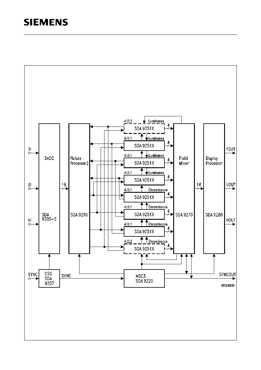
Introduction
The Field Mixer SDA 9270 is an add-on component for
the Siemens MEGAVISION IC set which enables the
system to reduce large area
and
line flickering of
interlaced TV standards.
1.1
Features
∑ High performance line flicker reduction algorithm
∑ Two input data formats (4:1:1 and 4:2:2)
SDA 9270
Semiconductor Group
5
1.2
Block Diagram
SDA 9270
Semiconductor Group
6
1.3
Pin Configuration

SDA 9270
Semiconductor Group
7
1.4
Pin Description
Pin No.
Name
Type
Description
10, 30, 47, 54, 70
V
SS
S
Supply voltage (
V
SS
) for digital parts and input
stages
11, 31, 48, 55, 71
V
DD
S
Supply voltage (
V
DD
) for digital parts and input
stages
74 .. 80,1
UVA0 .. 7 I/TTL
Data input UV of channel A (see Data Format)
2 .. 9
YA0 .. 7
I/TTL
Data input Y of channel A (see Data Format)
12 .. 19
UVB0 .. 7 I/TTL
Data input UV of channel B (see Data Format)
20 .. 27
YB0 .. 7
I/TTL
Data input Y of channel B (see Data Format)
28
RENB
Q/TTL
RAM enable field memory B
29
OEBB
Q/TTL
Output enable port B of field memory B
32
SACQ
Q/TTL
Serial column address output
33
SARQ
Q/TTL
Serial row address output
34
SCAD
I/TTL
Serial address clock input
35
SCA
I/TTL
Clock signal for data input
36
REN
I/TTL
RAM enable / input from SDA 9220
37
SACIN
I/TTL
Serial column address / input from SDA 9220
38
SARIN
I/TTL
Serial row address / input from SDA 9220
39
VS2
I/TTL
100 Hz vertical synchronization signal
40
BLN
I/TTL
Blanking signal, high level indicates active
video line
41
BLN2
I/TTL
Blanking signal / double line frequency
42
CLL
I/TTL
System clock
43.. 46,49..52
YQ0 .. 7
Q/TTL
Data output Y of channel Q (see Data Format)
53,56 .. 62
UVQ0 ..7
Q/TTL
Data output UV of channel Q (see Data
Format)
63
ZM
I/TTL
Zoom control input (HIGH level for zoom mode)
64
VS1
I/TTL
50 Hz vertical synchronization signal
65
TEST
I/TTL
Test pin; must be connected to
V
SS
for normal
operation
66
SCL
I
I
2
C-Bus clock line
67
SDA
IQ
I
2
C-Bus data line
SDA 9270
Semiconductor Group
8
Pin Description (cont'd)
S: supply,
I: input,
Q: output,
TTL: digital (TTL)
2
System Description
The device generates at its output an opportune sequence of 100/120 Hz fields derived
by processing the field A and the field B which are stored in 2 external field memories
and made available to the SDA 9270 on 2 separate input ports of 16 bit width each.
The device SDA 9270 generates also control signals for the SDA 9251 which are
necessary to operate the TV - SAMs in the Frame mode, that is to write the incoming
information alternatively in one or the other field memory.
Additionally the device generates a vertical sync pulse which has to be synchronized
with the respective field output. A horizontal blanking signal in phase with the output data
is also made available.
Pin No.
Name
Type
Description
68
BLN3
Q/TTL
Blanking signal / BLN2 delayed
69
VS3
Q/TTL
Vertical synchronization signal (switched
raster)
72
RENA
Q/TTL
RAM enable field memory A
73
OEBA
Q/TTL
Output enable port B of field memory A
SDA 9270
Semiconductor Group
9
2.1
Input Data Format
The SDA 9270 accepts for the input channels A and B two different input formats
(
I
2
C-Bus : INFOR) with two possible sample frequency relations of Y : (B-Y) : (R-Y). The
representation of the samples is programmable separately for luminance and
chrominance signals as positive dual code or 2's complement code (
I
2
C-Bus : INCODL,
INCODC)
X
ab
:
X: signal component
a: sample number
b: bit number
The amplitude resolution for each input signal component is 8 bit, the maximum clock
frequency is 30 MHz. Consequently the SDA 9270 is dedicated for applications in high
quality digital video systems. The data input stages and the internal data multiplexer
operate with a special input clock (SCA). For applications in the Siemens MEGAVISION
System the SCA-clock is identical with the memory output clock.
Data
Pin
Data Format 4:1:1
INFOR = 0
4:2:2 Parallel
INFOR = 1
Yx7
Y
07
Y
17
Y
27
Y
37
Y
07
Y
17
Yx6
Y
06
Y
16
Y
26
Y
36
Y
06
Y
16
Yx5
Y
05
Y
15
Y
25
Y
35
Y
05
Y
15
Yx4
Y
04
Y
14
Y
24
Y
34
Y
04
Y
14
Yx3
Y
03
Y
13
Y
23
Y
33
Y
03
Y
13
Yx2
Y
02
Y
12
Y
22
Y
32
Y
02
Y
12
Yx1
Y
01
Y
11
Y
21
Y
31
Y
01
Y
11
Yx0
Y
00
Y
10
Y
20
Y
30
Y
00
Y
10
Yx,UVx :
x : A,B
UVx7
U
07
U
05
U
03
U
01
U
07
V
07
UVx6
U
06
U
04
U
02
U
00
U
06
V
06
UVx5
V
07
V
05
V
03
V
01
U
05
V
05
UVx4
V
06
V
04
V
02
V
00
U
04
V
04
UVx3
U
03
V
03
UVx2
U
02
V
02
UVx1
U
01
V
01
UVx0
U
00
V
00
SDA 9270
Semiconductor Group
10
2.2
Output Data Format
The data format for the output channel Q will be a 4:2:2 parallel format in 2's complement
code representation.
X
ab
:
X: signal component
a: sample number
b: bit number
Data
Pin
4:2:2 Parallel
YQ7
Y
07
Y
17
YQ6
Y
06
Y
16
YQ5
Y
05
Y
15
YQ4
Y
04
Y
14
YQ3
Y
03
Y
13
YQ2
Y
02
Y
12
YQ1
Y
01
Y
11
YQ0
Y
00
Y
10
UVQ7
U
07
V
07
UVQ6
U
06
V
06
UVQ5
U
05
V
05
UVQ4
U
04
V
04
UVQ3
U
03
V
03
UVQ2
U
02
V
02
UVQ1
U
01
V
01
UVQ0
U
00
V
00

SDA 9270
Semiconductor Group
11
2.3
Field Interpolation and Switching
In order to reduce the annoying line and edge flickering a frame rate upconversion is
implemented. The upconversion includes a combination of interpolation algorithms
which are determined via
I
2
C-Bus and then selected automatically depending on the
picture motion content.
The field interpolation and switching block accepts at its input the data of the two
channels A and B, which are the combined luminance and chrominance information
respectively of the field A and the field B. The field rate is 100/120 Hz.
A fallback mode which corresponds to the operating mode AABB of the original
MEGAVISION system is made available. This mode is selected automatically in case of
non-standard input signals carrying unstable sync informations or it can be forced via
I
2
C-Bus.
2.4
Motion Detection
The motion detection output is switched in a 25/30 Hz frame synchronous raster. As
input signals for this block are accepted the luminance signal components of the input
channels A and B. By comparing the two fields the motion detector generates an
information about 3 possible motion content levels: LOW, MEDIUM and HIGH.
2.5
Field Memory Control
The Field Mixer SDA 9270 has to provide the two external field memories ≠ composed
of TV-SAM SDA 9251 ≠ with two pairs of control signals. One pair RENA and RENB
enables the MEGAVSION system to write the incoming field A and field B information
alternately into one field memory block and then into the other. A second pair of control
signals OEBA and OEBB enables alternately the output back channels of field memory
A and B for the noise reduction in the Picture Processor SDA 9290. Because of the
timing the serial address signals SAC and SAR generated by the MSC SDA 9220 must
be delayed by 4 SCAD-clock periods. This delay is implemented in the SDA 9270.
The Sync signals VS1 and BLN and the clock signal SCAD are used as timing reference
signals.
2.6
Frame Synchronization
In order to synchronize the data flows within field memories and Field Mixer and to
coordinate the signal information with the associated deflection control the Field Mixer
SDA 9270 has to generate 25 Hz picture frame sync signals.
One 25 Hz frame sync signal is necessary for generating the field memory control
signals RENA, RENB, OEBA, OEBB with a pattern repetition of 25 Hz each. This signal
is synchronized to the front end side video signal of the MEGAVISION block and uses
therefore as input signals the 50 Hz vertical sync signal VS1 generated by the MSC SDA
9220 and the horizontal blanking signal BLN.
SDA 9270
Semiconductor Group
12
A second 25 Hz frame sync signal is needed in the interpolation and switching block and
in the VS3 pulse generation block for assuring an output data sequence of the channel
Q synchronized with the VS3 pulse. As reference signals for this second frame sync
signal are used the 100 Hz vertical sync signal VS2 and the blanking signal BLN2 both
generated by the MSC SDA 9220.
2.7
SYNC-Signal Generation
This functional block generates a couple of sync signal needed in the processing stages
following the Field Mixer device. This couple includes the vertical sync signal VS3 and
the horizontal blanking signal BLN3. All these signals are synchronized with the output
channel Q.
2.8
I
2
C-Bus
2.8.1
I
2
C-Bus Address
2.8.2
I
2
C-Bus Format
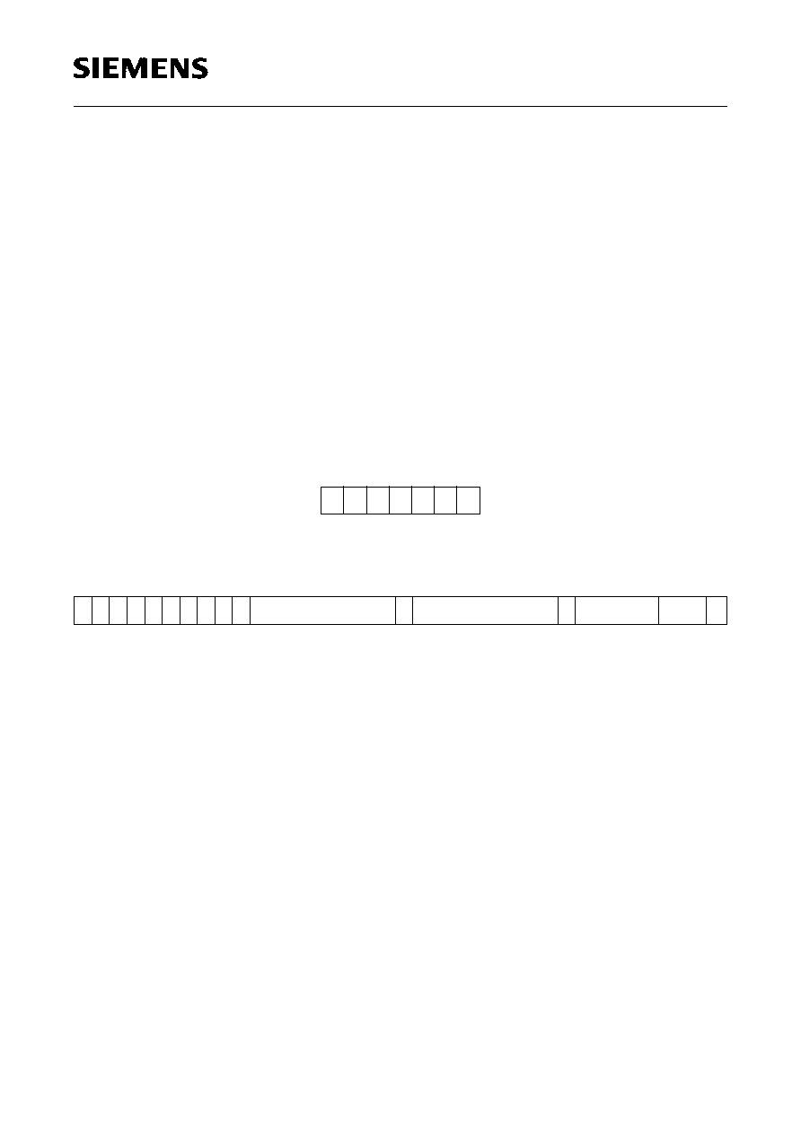
write:
S:
Start condition
A:
Acknowledge
P:
Stop condition
NA:
Not Acknowledge
An automatical address increment function is implemented.
0 0 0 1 1 1 1
S 0 0 0 1 1 1 1 0 A
Subaddress
A
Data Byte
A
*****
A
P
SDA 9270
Semiconductor Group
13
After switching on the IC (RES=0), all bits are set to defined states. Particularly:
Register
Default Value
Register
Default Value
00
00
H
0B
50
H
01
00
H
0C
03
H
02
00
H
0D
0D
H
03
00
H
0E
08
H
04
40
H
0F
28
H
05
F4
H
10
A5
H
06
58
H
11
55
H
07
20
H
12
0A
H
08
F8
H
13
18
H
09
70
H
14
05
H
0A
E8
H
15
03
H
SDA 9270
Semiconductor Group
14
2.8.3
I
2
C-Bus Commands
Sub-
add.
(Hex.)
Data Byte
D7
D6
D5
D4
D3
D2
D1
D0
00
LINFRA
PIXLIN
WRMODE2
WRMODE1
WRMODE0
NRDEL
RASTER1
RASTER0
01
0
INCODL
INCODC
INFOR
FALLBACK
FIWIN2
FIWIN1
FIWIN0
02
ZMMODE1
ZMMODE0
0
0
INTMODLL1
INTMODLL0 INTMODCL1
INTMODCL0
03
RDMODE1
RDMODE0
0
0
INTMODLM1 INTMODLM0 INTMODCM1
INTMODCM0
04
EDCONST1
EDCONST0
0
0
INTMODLH1 INTMODLH0 INTMODCH1
INTMODCH0
05
CFHENA07
CFHENA06
CFHENA05
CFHENA04
CFHENA03
CFHENA02
CFHENA01
CFHENA00
06
CFHENA17
CFHENA16
CFHENA15
CFHENA14
CFHENA13
CFHENA12
CFHENA11
CFHENA10
07
CFHENB07
CFHENB06
CFHENB05
CFHENB04
CFHENB03
CFHENB02
CFHENB01
CFHENB00
08
CFSCHA007 CFSCHA006 CFSCHA005 CFSCHA004 CFSCHA003 CFSCHA002 CFSCHA001
CFSCHA000
09
CFSCHA107 CFSCHA106 CFSCHA105 CFSCHA104 CFSCHA103 CFSCHA102 CFSCHA101
CFSCHA100
0A
CFSCHA017 CFSCHA016 CFSCHA015 CFSCHA014 CFSCHA013 CFSCHA012 CFSCHA011
CFSCHA010
0B
CFSCHA117 CFSCHA116 CFSCHA115 CFSCHA114 CFSCHA113 CFSCHA112 CFSCHA111
CFSCHA110
0C
CFSCHB007 CFSCHB006 CFSCHB005 CFSCHB004 CFSCHB003 CFSCHB002 CFSCHB001
CFSCHB000
0D
CFSCHB107 CFSCHB106 CFSCHB105 CFSCHB104 CFSCHB103 CFSCHB102 CFSCHB101
CFSCHB100
0E
CFSCHB017 CFSCHB016 CFSCHB015 CFSCHB014 CFSCHB013 CFSCHB012 CFSCHB011
CFSCHB010
SDA 9270
Semiconductor Group
15
I
2
C-Bus Commands (cont'd)
Sub-
add.
(Hex.)
Data Byte
D7
D6
D5
D4
D3
D2
D1
D0
0F
CFSCHB117
CFSCHB116
CFSCHB115
CFSCHB114
CFSCHB113
CFSCHB112
CFSCHB111
CFSCHB110
10
MDTHL21
MDTHL20
MDTHL11
MDTHL10
0
MDBLTH2
MDBLTH1
MDBLTH0
11
MDTHU21
MDTHU20
MDTHU11
MDTHU10
MDTHM21
MDTHM20
MDTHM11
MDTHM10
12
0
0
HYTHL15
HYTHL14
HYTHL13
HYTHL12
HYTHL11
HYTHL10
13
0
0
HYTHL25
HYTHL24
HYTHL23
HYTHL22
HYTHL21
HYTHL20
14
0
0
HYTHH15
HYTHH14
HYTHH13
HYTHH12
HYTHH11
HYTHH10
15
0
0
HYTHH25
HYTHH24
HYTHH23
HYTHH22
HYTHH21
HYTHH20

SDA 9270
Semiconductor Group
16
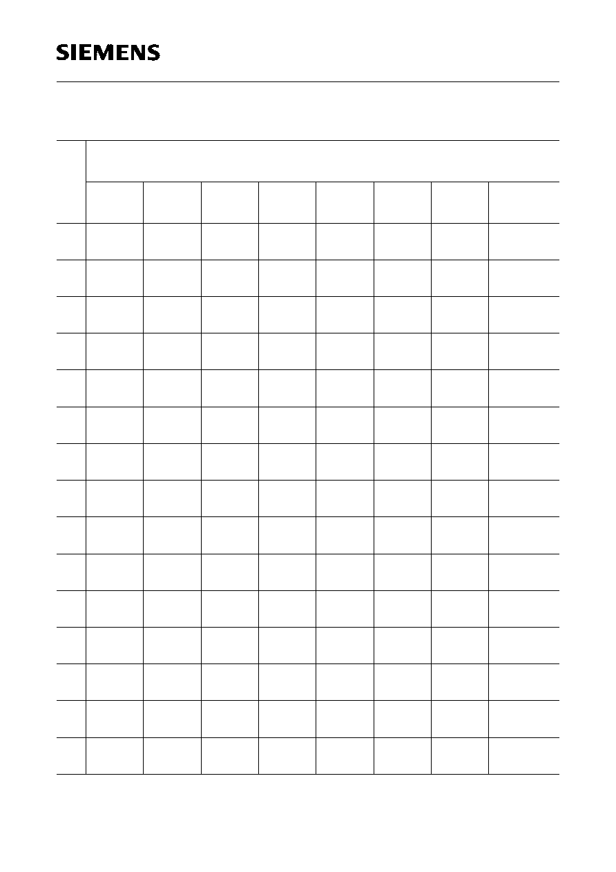
2.8.4
Detailed Description
Note: SDA 9220 programming:
≠ Subaddress 00 / D7 (EXSYN): For EXSYN=1 WRMODE=100 is required.
≠ Subaddress 01 / D7 (FLDM), Subaddress 02 / D7 (STB): FLDM and STB should
always be set to 0.
≠ Subaddress 00 / D1, D0 (VDM): VDM must be set to 00.
Subaddress 00
Bit
Name
Function
D7
LINFRA
Lines per frame:
0 :
625 lines per frame (default value)
1 :
525 lines per frame
D6
PIXLIN
Pixels per line:
0 :
864 pixels per line (default value)
1 :
858 pixels per line
D5...D3
WRMODE*
Write Mode:
000 :
Normal operation: field memory A and field memory B
are written alternately (default value)
001 :
Still picture A and B: writing is suppressed for both
field memories
010 :
Still picture A: writing is suppressed for field memory A,
all incoming fields are written to field memory B
011 :
Still picture A: writing is suppressed for field memory A,
every second field is written to field memory B
(Field Mode B)
100 :
Still picture B: writing is suppressed for field memory B,
all incoming fields are written to field memory A
101 :
Still picture B: writing is suppressed for field memory B,
every second field is written to field memory A
(Field Mode A)
110 :
Reserved
111 :
Reserved
D2
NRDEL
Noise Reduction Delay:
conditions: 2 field memory configuration, WRMODE = 000
0:
Data delay for recursive filtering is one frame
(default value)
1:
Data delay for recursive filtering is one field
D1...D0
RASTER*
Deflection Raster control:
00:
Control by interpolation algorithm (default value)
01:
10:
11:

SDA 9270
Semiconductor Group
17
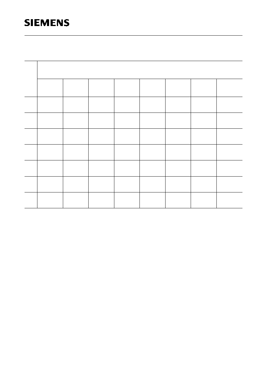
Subaddress 01
Bit
Name
Function
D6
INCODL
Coding of luminance input data:
0:
positive dual code (default value)
1:
2's complement
D5
INCODC
Coding of chrominance input data:
0:
positive dual code (default value)
1:
2's complement
D4
INFOR
Input data format:
0:
4:1:1 luminance, chrominance parallel (8+4 wires)
(default value)
1:
4:2:2 luminance, chrominance parallel (8+8 wires)
D3
FALLBACK
Fallback mode:
0:
Normal operation (default value)
1:
programmed fall back mode is activated for current
display
D2...D0
FIWIN
Field identification window
Definition of a time window. Switching from fall back mode to
programmed display mode is not performed until the field
identification algorithm is working in a stable condition
during the programmed time.
000 :
7 field periods (default value)
001 :
15 field periods
:
:
110 :
55 field periods
111 :
63 field periods

SDA 9270
Semiconductor Group
18
Subaddress 02
Bit
Name
Function
D7..D6
ZMMODE
zoom mode (enabled only if pin ZM = 1 and
RDMODE = 00)
00:
field sequence at output Q: AABB (default value)
01:
field sequence at output Q: ABAB
10:
display with raster correction
11:
Reserved
D3..D2
INTMODLL
luminance interpolation mode, low degree of motion
00:
field sequence AABB without interpolation (
)
(default value)
01:
field sequence ABAB without interpolation (
)
10:
Schrˆder algorithm (
)
11:
Hentschel algorithm (
)
D1..D0
INTMODCL
chrominance interpolation mode, low degree of motion
00:
field sequence AABB without interpolation (
)
(default value)
01:
field sequence AABB without interpolation (
)
10:
field sequence ABAB without interpolation (
)
11:
linear interpolation (
)

SDA 9270
Semiconductor Group
19
Subaddress 03
Bit
Name
Function
D7..D6
RDMODE
read mode
00:
both inputs are used
(interpolation enabled if ZM = 0)
(default value)
01:
only input A is used (without interpolation)
10:
only input B is used (without interpolation)
11:
Reserved
D3..D2
INTMODLM
luminance interpolation mode, medium degree of motion
00:
field sequence AABB without interpolation (
)
(default value)
01:
field sequence ABAB without interpolation (
)
10:
Schrˆder algorithm (
)
11:
Hentschel algorithm (
)
D1..D0
INTMODCM
chrominance interpolation mode, medium degree of motion
00:
field sequence AABB without interpolation (
)
(default value)
01:
field sequence AABB without interpolation (
)
10:
field sequence ABAB without interpolation (
)
11:
linear interpolation (
)
SDA 9270
Semiconductor Group
20
Subaddress 04
Bit
Name
Function
D7..D6
EDCONST
edge detector gain factor
00:
2
01:
3 (default value)
10:
4
11:
5
D3..D2
INTMODLH
luminance interpolation mode, high degree of motion
00:
field sequence AABB without interpolation (
)
(default value)
01:
field sequence ABAB without interpolation (
)
10:
Schrˆder algorithm (
)
11:
Hentschel algorithm (
)
D1..D0
INTMODCH
chrominance interpolation mode, high low degree of motion
00:
field sequence AABB without interpolation (
)
(default value)
01:
field sequence AABB without interpolation (
)
10:
field sequence ABAB without interpolation (
)
11:
linear interpolation (
)
Subaddress 05
Bit
Name
Function
D7..D0
CFHENA0
Hentschel algorithm, 8-bit coefficient a
0
(2's complement)
(default value F4
H
)
Subaddress 06
Bit
Name
Function
D7..D0
CFHENA1
Hentschel algorithm, 8-bit coefficient a
1
(2's complement)
(default value 58
H
)
SDA 9270
Semiconductor Group
21
Subaddress 07
Bit
Name
Function
D7..D0
CFHENB0
Hentschel algorithm, 8-bit coefficient b
0
(2's complement)
(default value 20
H
)
Subaddress 08
Bit
Name
Function
D7..D0
CFSCHA00
Schrˆder algorithm, 8-bit coefficient a
00
(2's complement)
(default value F8
H
)
Subaddress 09
Bit
Name
Function
D7..D0
CFSCHA10
Schrˆder algorithm, 8-bit coefficient a
10
(2's complement)
(default value 70
H
)
Subaddress 0A
Bit
Name
Function
D7..D0
CFSCHA01
Schrˆder algorithm, 8-bit coefficient a
01
(2's complement)
(default value E8
H
)
Subaddress 0B
Bit
Name
Function
D7..D0
CFSCHA11
Schrˆder algorithm, 8-bit coefficient a
11
(2's complement)
(default value 50
H
)
Subaddress 0C
Bit
Name
Function
D7..D0
CFSCHB00
Schrˆder algorithm, 8-bit coefficient b
00
(2's complement)
(default value 03
H
)
SDA 9270
Semiconductor Group
22
Subaddress 0D
Bit
Name
Function
D7..D0
CFSCHB10
Schrˆder algorithm, 8-bit coefficient b
10
(2's complement)
(default value 0D
H
)
Subaddress 0E
Bit
Name
Function
D7..D0
CFSCHB01
Schrˆder algorithm, 8-bit coefficient b
01
(2's complement)
(default value 08
H
)
Subaddress 0F
Bit
Name
Function
D7..D0
CFSCHB11
Schrˆder algorithm, 8-bit coefficient b
11
(2's complement)
(default value 28
H
)
Subaddress 10
Bit
Name
Function
D7..D6
MDTHL2
threshold for low degree of motion (small blocks)
00:
0
01:
64
10:
128 (default value)
11:
192
D5..D4
MDTHL1
threshold for low degree of motion (large blocks)
00:
0
01:
64
10:
128 (default value)
11:
192
D2..D0
MDBLTH
threshold in front of the blocking module
000:
4
001:
8
:
:
111:
32
(default value 101)

SDA 9270
Semiconductor Group
23
Subaddress 11
Bit
Name
Function
D7..D6
MDTHU2
threshold for high degree of motion (small blocks)
00:
384
01:
512 (default value)
10:
640
11:
768
D5..D4
MDTHU1
threshold for high degree of motion (large blocks)
00:
384
01:
512 (default value)
10:
640
11:
768
D3..D2
MDTHM2
threshold for second field difference (small blocks)
00:
64
01:
128 (default value)
10:
192
11:
256
D1..D0
MDTHM1
threshold for second field difference (large blocks)
00:
64
01:
128 (default value)
10:
192
11:
256
Subaddress 12
Bit
Name
Function
D5..D0
HYTHL1
hysteresis threshold, low degree of motion (large blocks)
000000:
1
000001:
1
000010:
2
:
111111:
63
(default value 001010)
SDA 9270
Semiconductor Group
24
Subaddress 13
Bit
Name
Function
D5..D0
HYTHL2
hysteresis threshold, low degree of motion (small blocks)
000000:
1
000001:
1
000010:
2
:
111111:
63
(default value 011000)
Subaddress 14
Bit
Name
Function
D5..D0
HYTHH1
hysteresis threshold, high degree of motion (large blocks)
000000:
1
000001:
1
000010:
2
:
111111:
63
(default value 000101)
Subaddress 15
Bit
Name
Function
D5..D0
HYTHH2
hysteresis threshold, high degree of motion (small blocks)
000000:
1
000001:
1
000010:
2
:
111111:
63
(default value 000011)

SDA 9270
Semiconductor Group
25
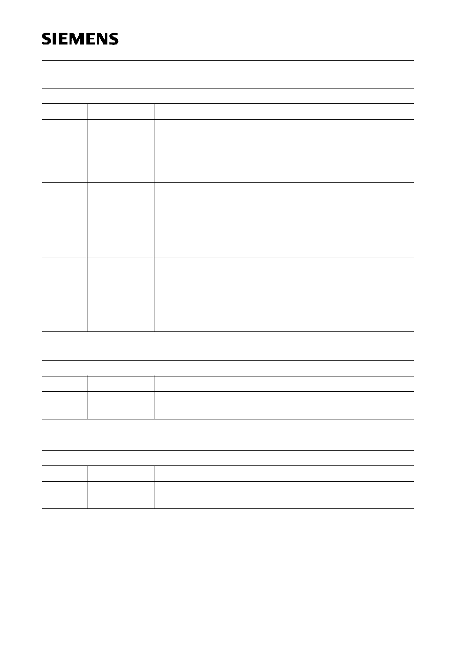
3
Electrical Characteristics
3.1
Absolute Maximum Ratings
All voltages listed are referenced to ground (0 V,
V
SS
) except where noted.
Note: Absolute Maximum Ratings are those values beyond which damage to the device
may occur. Functional operation under these conditions or at any other condition
beyond those indicated in the operational sections of this specification is not
implied.
Maximum ratings are absolute ratings; exceeding only one of these values may
cause irreversible damage to the integrated circuit.
Parameter
Symbol
Limit Values
Unit
Remark
min.
max.
Operating temperature
T
A
0
70
∞C
Storage temperature
T
stg
-
65
125
∞C
Junction temperature
T
j
125
∞C
Soldering temperature
T
S
260
∞C
Soldering time
t
S
10
s
Input voltage
V
I
-
0.3 V
V
DD
+ 0.3 V V
V
CC
respectively
Output voltage
V
Q
-
0.3 V
V
DD
+ 0.3 V V
V
CC
respectively
Supply voltages
V
S
-
0.3
6
V
Supply voltage
Differentials
V
-
0.25
0.25
V
between any
internally non-
connected supply pins
of the same kind, see
Pin Description
Total power dissipation
P
tot
1
W
ESD protection
ESD
-
2
2
kV
MIL STD 883C
method 3015.6,
100 pF, 1500
Latch-up protection
-
100
100
mA
all inputs/outputs
SDA 9270
Semiconductor Group
26
3.2
Recommended Operating Conditions
Parameter
Symbol
Limit Values
Unit
Test
Conditions
min.
typ.
max.
Supply voltages
V
DD
V
CC
4.5
5
5.5
V
Ambient temperature
T
A
0
25
70
∞C
All TTL Inputs
High-level input voltage
V
IH
2.0 V
V
DD
1
Low-level input voltage
V
IL
0
0.8
V
All TTL outputs
High-level output voltage
V
QH
2.4
V
I
QH
=
-
2.0 mA
Low-level output voltage
V
QL
0.4
V
I
QL
= 3.0 mA
Clock TTL Inputs CLL, SCA, SCAD
Clock frequency
12
27
30
MHz
Low time
t
WL
10
ns
Rise/fall time
5 ns
High time
t
WH
10
ns
Rise time
t
TLH
5
ns
Fall time
t
THL
5
ns
SCA - CLL skew time
t
SK
0
15
ns
Diagram
on page 22
I
2
C Bus (all values are referred to min(
V
IH
) and max(
V
IL
))
High-level input voltage
V
IH
3 V
V
DD
1
Low-level input voltage
V
IL
0
1.5
V
SCL clock frequency
f
SCL
0
400
kHz
Inactive time before start of
transmission
t
BUF
1.3
µ
s
Set-up time start condition
t
SU;STA
0.6
µ
s
Hold time start condition
t
HD;STA
0.6
µ
s
SCL low time
t
LOW
1.3
µ
SCL high time
t
HIGH
0.6
µ
s
Set-up time DATA
t
SU;DAT
100
ns
SDA 9270
Semiconductor Group
27
Note: Under this conditions the functions given in the circuit description are fulfilled.
Nominal conditions specify mean values expected over the production spread and
are the proposed values for interface and application. If not stated otherwise,
nominal values will apply at
T
A
= 25 ∞C and the nominal supply voltage.
Hold time DATA
t
HD;DAT
0
µ
s
SDA/SCL rise times
t
R
300
ns
f
SCL
= 400 kHz
SDA/SCL fall times
t
F
300
ns
Set-up time stop condition
t
SU;STO
0.6
µ
s
Low-level output current
I
OL
3
mA
3.2
Recommended Operating Conditions (cont'd)
Parameter
Symbol
Limit Values
Unit
Test
Conditions
min.
typ.
max.
SDA 9270
Semiconductor Group
28
3.3
Characteristics (Assuming Recommended Operating Conditions)
Parameter
Symbol
Limit Values
Unit
Remark
min.
max.
Average supply current
I
S
200
mA
All
V
CC
and
V
DD
pins
All Digital Inputs (including I/O inputs)
Input capacitance
C
I
10
pF
Not tested;
max. 7 pF for SCA, CLL
Input leakage current
I
I
-
10
10
µ
A
TTL Inputs: YA, YB, UVA, UVB (referenced to SCA)
Set-up time
t
SU
7
ns
Input hold time
t
IH
6
ns
TTL Inputs: REN, SACIN, SARIN (referenced to SCAD)
Set-up time
t
SU
7
ns
Input hold time
t
IH
6
ns
TTL Inputs: BLN, BLN2, VS1, VS2, ZM (referenced to CLL)
Note: For BLN a jitter of
±
1 CLL is allowed
Set-up time
t
SU
7
ns
Input hold time
t
IH
6
ns
TTL Outputs: YQ, UVQ (referenced to CLL)
Hold time
t
QH
6
ns
Delay time
t
QD
25
ns
C
L
= 30 pF
TTL Outputs: VS3, BLN3 (referenced to CLL)
Hold time
t
QH
6
ns
Delay time
t
QD
25
ns
C
L
= 30 pF
TTL Outputs: RENA, RENB, SACQ, SARQ (referenced to SCAD)
Hold time
t
QH
6
ns
Delay time
t
QD
20
ns
C
L
= 50 pF
SDA 9270
Semiconductor Group
29
Note: The listed characteristics are ensured over the operating range of the integrated
circuit.
TTL Outputs: OEBA, OEBB (referenced to SCAD)
Hold time
t
QH
6
ns
Delay time
t
QD
20
ns
C
L
= 30 pF
Input/Output: SDA (referenced to SCL; Open Drain Output)
Low-level output voltage
V
OL
0.5
V
at
I
OL
= max
3.3
Characteristics (Assuming Recommended Operating Conditions) (cont'd)
Parameter
Symbol
Limit Values
Unit
Remark
min.
max.
SDA 9270
Semiconductor Group
30
4
Application Information
SDA 9270
Semiconductor Group
31
5
Waveforms
Timing Diagram Data Input/Output Referenced to the Clock
Timing Diagram Clock Skew SCA - CLL
SDA 9270
Semiconductor Group
32
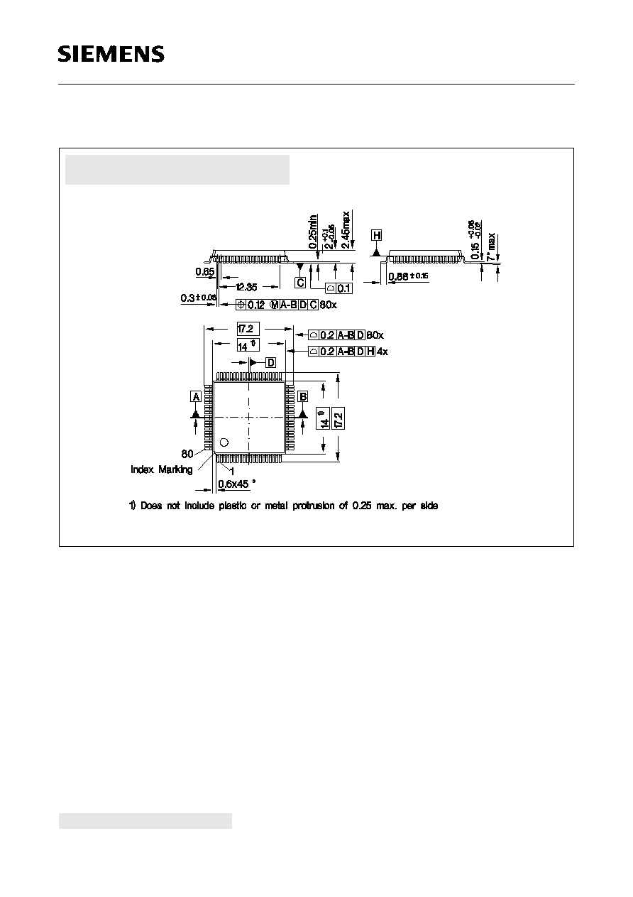
6
Package Outlines
P-MQFP-80-1
(Plastic Metric Quad Flat Package)
GPM05249
Sorts of Packing
Package outlines for tubes, trays etc. are contained in our
Data Book "Package Information".
Dimensions in mm
SMD = Surface Mounted Device

SDA 9270
Semiconductor Group
33