 | –≠–ª–µ–∫—Ç—Ä–æ–Ω–Ω—ã–π –∫–æ–º–ø–æ–Ω–µ–Ω—Ç: SDA9361 | –°–∫–∞—á–∞—Ç—å:  PDF PDF  ZIP ZIP |

ICs for Consumer Electronics
DDC-PLUS-Deflection Controller
SDA 9361
Data Sheet 1998-02-01

Edition 1998-02-01
This edition was realized using
the software system FrameMaker
Æ
Published by Siemens AG, Bereich
Halbleiter, Marketing-Kommunikation,
Balanstraþe 73,
81541 M¸nchen
©
Siemens AG 1998.
All Rights Reserved.
Attention please!
As far as patents or other rights of third
parties are concerned, liability is only
assumed for components, not for
applications, processes and circuits
implemented within components or
assemblies.
The information describes the type of
component and shall not be considered
as assured characteristics.
Terms of delivery and rights to change
design reserved.
For questions on technology, delivery
and prices please contact
the Semiconductor Group Offices in
Germany or the Siemens Companies and
Representatives worldwide
(see address list).
Due to technical requirements compo-
nents may contain dangerous substanc-
es. For information on the types in ques-
tion please contact your nearest
Siemens Office, Semiconductor Group.
Siemens AG is an approved CECC man-
ufacturer.
Packing
Please use the recycling operators
known to you. We can also help you ≠ get
in touch with your nearest sales office. By
agreement we will take packing material
back, if it is sorted. You must bear the
costs of transport.
For packing material that is returned to us
unsorted or which we are not obliged to
accept, we shall have to invoice you for
any costs incurred.
Components used in life-support de-
vices or systems must be expressly
authorized for such purpose!
Critical components
1
of the Semiconduc-
tor Group of Siemens AG, may only be
used in life-support devices or systems
2
with the express written approval of the
Semiconductor Group of Siemens AG.
1 A critical component is a component
used in a life-support device or system
whose failure can reasonably be
expected to cause the failure of that
life-support device or system, or to
affect its safety or effectiveness of that
device or system.
2 Life support devices or systems are
intended (a) to be implanted in the
human body, or (b) to support and/or
maintain and sustain human life. If
they fail, it is reasonable to assume
that the health of the user may be
endangered.

Data Classification
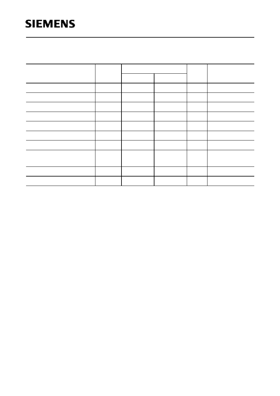
Maximum Ratings
Maximum ratings are absolute ratings; exceeding only one of these values may cause
irreversible damage to the integrated circuit.
Recommended Operating Conditions
Under this conditions the functions given in the circuit description are fulfilled. Nominal
conditions specify mean values expected over the production spread and are the
proposed values for interface and application. If not stated otherwise, nominal values will
apply at
T
A
=25∞C and the nominal supply voltage.
Characteristics
The listed characteristics are ensured over the operating range of the integrated circuit.
Edition 1998-02-01
Published by Siemens AG, Semiconductor Group
Copyright
©
Siemens AG 1998. All rights reserved.
Terms of delivery and right to change design reserved.
SDA 9361
Revision History:
Current Version: 1998-02-01
Previous Version:
1997-04-07
Page
(in previous
Version)
Page
(in current
Version)
Subjects (major changes since last revision)
33
35
Setup time of input HSYNC (CLEXT=1) changed from 6 ns to 4 ns
35
37
Nom. average and max. stand-by current specified
35
37
Specification of charge current pump of PLL pin LF is unnecessary

SDA 9361
Table of Contents
Page
Semiconductor Group
4
1998-02-01
1
Overview . . . . . . . . . . . . . . . . . . . . . . . . . . . . . . . . . . . . . . . . . . . . . . . . . . . . 5
1.1
Features . . . . . . . . . . . . . . . . . . . . . . . . . . . . . . . . . . . . . . . . . . . . . . . . . . . . . 5
1.2
General Description . . . . . . . . . . . . . . . . . . . . . . . . . . . . . . . . . . . . . . . . . . . . 6
1.3
Pin Configuration . . . . . . . . . . . . . . . . . . . . . . . . . . . . . . . . . . . . . . . . . . . . . . 6
1.4
Pin Description . . . . . . . . . . . . . . . . . . . . . . . . . . . . . . . . . . . . . . . . . . . . . . . . 7
1.5
Block Diagram . . . . . . . . . . . . . . . . . . . . . . . . . . . . . . . . . . . . . . . . . . . . . . . . 9
2
System Description . . . . . . . . . . . . . . . . . . . . . . . . . . . . . . . . . . . . . . . . . . 10
2.1
Functional Description . . . . . . . . . . . . . . . . . . . . . . . . . . . . . . . . . . . . . . . . . 10
2.2
Circuit Description . . . . . . . . . . . . . . . . . . . . . . . . . . . . . . . . . . . . . . . . . . . . 12
2.3
Reset Modes . . . . . . . . . . . . . . . . . . . . . . . . . . . . . . . . . . . . . . . . . . . . . . . . 14
2.4
Frequency Ranges . . . . . . . . . . . . . . . . . . . . . . . . . . . . . . . . . . . . . . . . . . . . 15
2.5
I≤C-Bus Control . . . . . . . . . . . . . . . . . . . . . . . . . . . . . . . . . . . . . . . . . . . . . . 16
2.5.1
I≤C-Bus Address . . . . . . . . . . . . . . . . . . . . . . . . . . . . . . . . . . . . . . . . . . . . . . 16
2.5.2
I≤C-Bus Format . . . . . . . . . . . . . . . . . . . . . . . . . . . . . . . . . . . . . . . . . . . . . . . 16
2.5.3
I≤C-Bus Commands . . . . . . . . . . . . . . . . . . . . . . . . . . . . . . . . . . . . . . . . . . . 17
2.5.4
Detailed Description . . . . . . . . . . . . . . . . . . . . . . . . . . . . . . . . . . . . . . . . . . . 18
2.5.5
Explanation of Some Control Items . . . . . . . . . . . . . . . . . . . . . . . . . . . . . . . 24
3
Absolute Maximum Ratings . . . . . . . . . . . . . . . . . . . . . . . . . . . . . . . . . . . 33
3.1
Recommended Operating Conditions . . . . . . . . . . . . . . . . . . . . . . . . . . . . . 34
3.2
Characteristics (Assuming Recommended Operating Conditions) . . . . . . . 37
4
Application Information . . . . . . . . . . . . . . . . . . . . . . . . . . . . . . . . . . . . . . . 40
5
Waveforms . . . . . . . . . . . . . . . . . . . . . . . . . . . . . . . . . . . . . . . . . . . . . . . . . 41
5.1
VD- Output Voltage, 4/3-CRT and 16/9-Source . . . . . . . . . . . . . . . . . . . . . . 41
5.2
Timing Diagram of SCAN . . . . . . . . . . . . . . . . . . . . . . . . . . . . . . . . . . . . . . . 42
5.3
Power On/Off Diagram . . . . . . . . . . . . . . . . . . . . . . . . . . . . . . . . . . . . . . . . . 44
5.4
Standby Mode, RESN Diagram . . . . . . . . . . . . . . . . . . . . . . . . . . . . . . . . . . 45
5.5
Function of H,V Protection . . . . . . . . . . . . . . . . . . . . . . . . . . . . . . . . . . . . . . 46
6
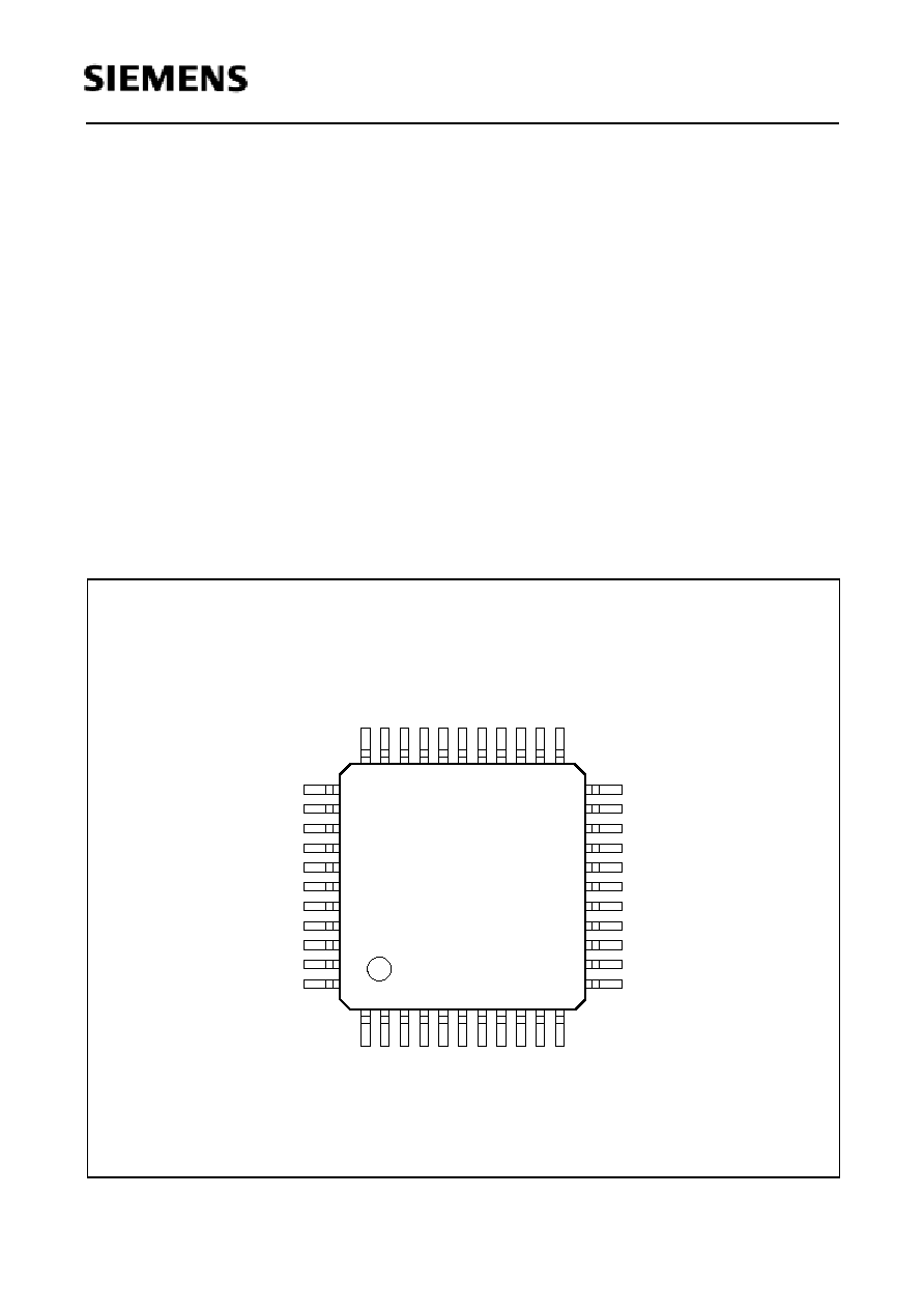
Package Outlines . . . . . . . . . . . . . . . . . . . . . . . . . . . . . . . . . . . . . . . . . . . . 47
P-MQFP-44-2
Semiconductor Group
5
1998-02-01
DDC-PLUS-Deflection Controller
SDA 9361
MOS
Type
Ordering Code
Package
SDA 9361
Q67107-H5167-A703
P-MQFP-44-2
1
Overview
1.1
Features
∑ Deflection - Protection - 16:9 / 4:3
∑ No external clock needed
∑
1
PLL and
2
PLL on chip
∑
2
C-Bus alignment of all deflection parameters
∑ All EW-, V- and H- functions
∑ PW EHT compensation
∑ PH EHT compensation
∑ Compensation of H-phase deviation (e.g. caused by white bar)
∑ Upper/lower EW-corner correction separately adjustable
∑ V-angle correction: Vertical frequent linear modulation of H-phase
∑ V-bow correction: Vertical frequent parabolic modulation of H-phase
∑ Three reduced V-scan modes (75 %, 66 %, 50 % V-size) adjustable by only 2 Bits
∑ H-frequent PWM output signal for general purpose
∑ H- and V-blanking time adjustable
∑ Partial overscan adjustable to hide the cut off control measuring lines in the
reducedscan modes
∑ Stop/start of vertical deflection adjustable to fill out the 16/9 screen with different
letterbox formats without annoying overscan
∑ Control signal SCAN as reference for vertical positioning of OSD, PIP etc.
∑ Vertical noise reduction with memory
∑ Standard and doubled line frequencies for NTSC and PAL, MUSE standard,
ATV standard, HDTV standard
∑ Self adaptation of V-frequency/number of lines per field between 192 and 680 for each
possible line frequency
∑ Protection against EHT run away (X-rays protection)
SDA 9361
Semiconductor Group
6
1998-02-01
∑ Protection against missing V-deflection (CRT-protection)
∑ Selectable softstart of the H-output stage
∑ Clock generation on chip
∑ P-MQFP-44-2 package
∑ 5 V supply voltage
1.2
General Description
The SDA 9361 is a highly integrated deflection controller for CTV receivers with standard
or doubled line and field frequencies. It controls among others an horizontal driver circuit
for a flyback line output stage, a DC coupled vertical saw-tooth output stage and an east/
west raster correction circuit. All adjustable output parameters are
2
C Bus controlled.
Inputs are HSYNC and VSYNC. The HSYNC signal is the reference for the internal clock
system which includes the
1 and
2 control loops.
1.3
Pin Configuration
Figure 1
UEP10278
HSYNC
11
1 2 3 4 5 6 7 8 9 10
33
12
44
32 31 30 29 28 27 26 25 24 23
43
13
42
14
41
15
40
16
39
17
38
18
37
19
36
20
35
21
34
22
SELFH1_2
CLKI
X2
SDAT
V
DD(D)
SS(D)
V
X1
SCLK
SCAN
RESN
SCP
E/W
V
DD(A2)
V
REFP
REFN
V
SSA(1)
V
ABL
D/A
DDA(1)
V
HPROT
CLEXT
FH1_2
TEST
HD
PWM
REFH
V
REFL
V
SS(A2)
V
DD(A3)
V
REFC
V
SS(A3)
V
DD(D)
V
V
SS(D)
SSD
SS(A4)
V
LF
DD(A4)
V
VOFFD
VPROT
VD+
VD-
VSYNC
2
SDA 9361
Semiconductor Group
7
1998-02-01
1.4
Pin Description
Pin No. Symbol
Type
Description
1
CLKI
I/TTL
Input for external clock
2
X1
I
Reference oscillator input, crystal
3
X2
Q
Reference oscillator output, crystal
4
SDAT
IQ
2
C-Bus data
5
SCLK
I
2
C-Bus clock
6
RESN
I/TTL
Reset input, active low
7
SCAN
Q/TTL
Control signal for vertical positioning of OSD, PIP etc.
8
SCP
Q
Blanking signal with H- and color burst component
(V-component selectable by
2
C Bus)
9
V
DD(D)
S
Digital supply
10
V
SS(D)
S
Digital ground
11
VPROT
I
Watching external V-output stage (input is the V-saw-
tooth from feedback resistor)
12
HPROT
I
Watching EHT (input is e.g. H-flyback)
13
V
DD(A1)
S
Analog supply
14
D/A
Q
Output of an
2
C Bus controlled DC voltage
15
ABL
I
Input for a beam current dependent signal for
stabilization of width, height and H-phase
16
V
SS(A1)
S
Analog ground
17
V
REFN
IQ
Ground for
V
REFP
,
V
REFH
,
V
REFL
18
V
REFP
IQ
Reference voltage for IBEAM ADC, DAC, HPROT /
VPROT thresholds
19
V
DD(A2)
S
Analog supply
20
E/W
Q
Control signal output for east/west raster correction
21
VD+
Q
Control signal output for DC coupled V-output stage
22
VD-
Q
Like VD+
23
V
SS(A2)
S
Analog ground
24
V
REFL
IQ
Reference voltages for E/W-DAC, V-DAC
25
V
REFH
IQ
Like
V
REFL
26
2
I
Line flyback for H-delay compensation
27
PWM
Q/TTL
Control signal output
SDA 9361
Semiconductor Group
8
1998-02-01
1.4
Pin Description
(cont'd)
1)
The external clock mode can not be used with 33.75 kHz and 35 kHz line frequency.
Pin No. Symbol
Type
Description
28
VSYNC
I/TTL
V-sync input
29
HD
Q
Control signal output for H driver stage
30
TEST
I/TTL
Switching normal operation (TEST = L) and test mode
(TEST = H: pins 7, 27, 31, 32, 33, 40, 44 are additional
test pins)
31
FH1_2
I/TTL
Switching between 1F
H
mode (L) and 2F
H
mode (H)
(Pin SELFH1_2 = 0)
32
CLEXT
I/TTL
Switching between internal (L) and external clock (H)
1)
33
SELFH1_2 I/TTL
Selection of switching between 1F
H
mode and 2F
H
mode
SELFH1_2 = 0:1F
H
/2F
H
selected via pin FH1_2
SELFH1_2 = 1:1F
H
/2F
H
selected via
2
C-Bus register 00
H
, Bit D5
34
V
DD(A3)
S
Analog supply
35
HSYNC
I
HSYNC input (CLEXT = 1: TTL; CLEXT = 0: analog)
1)
36
V
REFC
I
Reference voltage for sync ADC
37
V
SS(A3)
S
Analog ground
38
V
DD(D)
S
Digital supply
39
V
SS(D)
S
Digital ground
40
SSD
I/TTL
Disables softstart
41
V
SS(A4)
S
Analog ground
42
LF
IQ
PLL loop filter
43
V
DD(A4)
S
Analog supply
44
VOFFD
I/TTL
Defines default value of VOFF-Bit
(
2
C-Bus register 00
H
, Bit D7)
SDA 9361
Semiconductor Group
9
1998-02-01
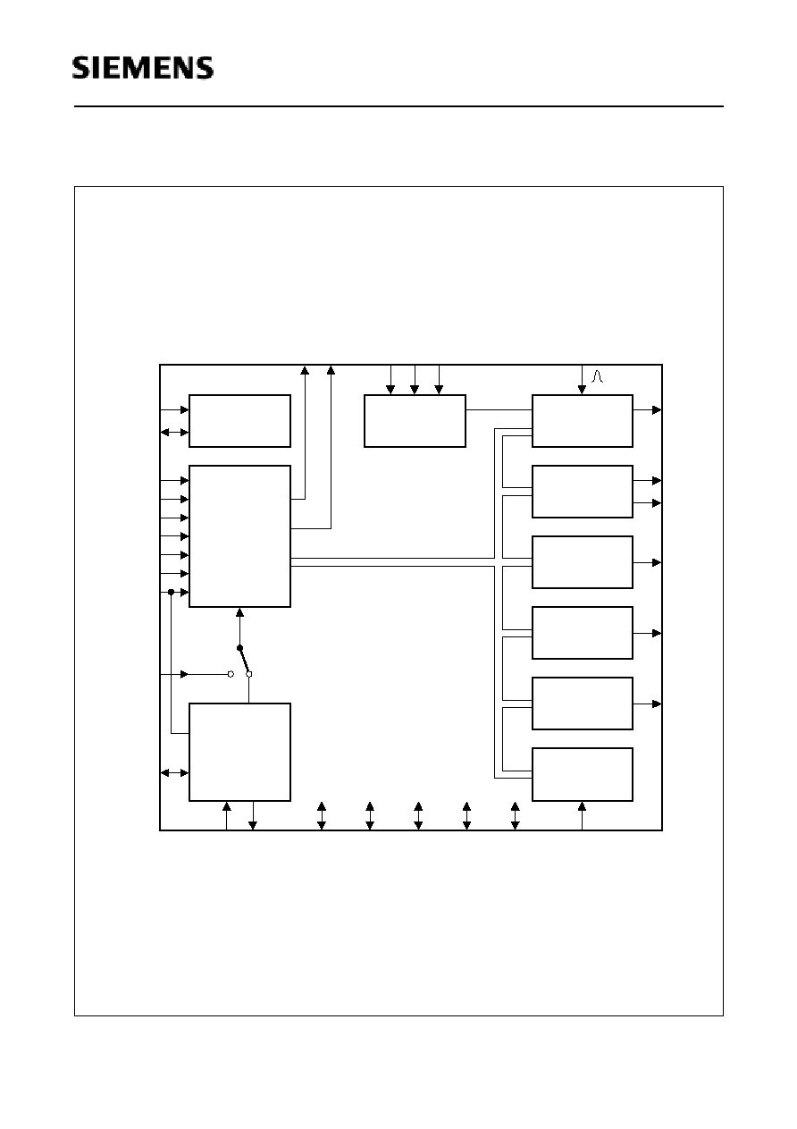
1.5
Block Diagram
Figure 2
UEB10277
2
C
Protection
Start Up
Control
H-Out
V-Out
EW-Corr
PWM
D/A
PW/PH Corr
PLL
CLL
SCP SCAN HPROT SSD VPROT
2
SCLK
SDAT
VOFFD
SELFH1_2
TEST
FH1_2
CLEXT
VSYNC
HSYNC
CLKI
LF
HD
E/W
PWM
D/A
ABL
REFN
V
REFP
V
REFH
V
REFL
V
REFC
V
X1 X2
VD+
VD-

SDA 9361
Semiconductor Group
10
1998-02-01
2
System Description
2.1
Functional Description
The main input signals are HSYNC with standard or doubled horizontal frequency and
VSYNC with vertical frequencies of 50/100 Hz or 60/120 Hz.
The VSYNC is processed in a noise reduction circuit to enable synchronization by worse
transmission too.
The output signals control the horizontal as well as the vertical deflection stages and the
east/west raster correction circuit.
The H-output signal HD compensates the delays of the line output stage and its phase
can be modulated vertical frequent to remove horizontal distortions of vertical raster lines
(V-Bow, V-Angle). Time reference is the middle of the front and back edge of the line
flyback pulse. A positive HD pulse switches off the line output transistor. Maximal H-shift
is about 4.5
µ
s (for 1F
H
) or 2.25
µ
s (for 2F
H
).
Picture tubes with 4:3 or 16:9 aspect ratio can be used by adapting the raster to the
aspect ratio of the source signal.
The V-output saw-tooth signals VD- and VD+ controls a DC coupled output stage and
can be disabled. Suitable blanking signals are delivered by the IC.
The east/west output signal E/W is a vertical frequent parabola of 4th order, enabling an
additional corner correction, separately for the upper and lower part.
The pulse width modulated horizontal frequent output signal PWM is for optional use. It
can be modulated between 1 and 215 steps. The step width is 4
*
t
H
/864.
The output D/A delivers a variable DC signal for general purpose.
The picture width and picture height compensation (PW/PH Comp) processes the beam
current dependent input signal ABL with effect to the outputs E/W and VD to keep width
and height constant and independent of brightness.
The alignment parameter Horizontal Shift Compensation enables to adjust the influence
of the input signal ABL on the horizontal phase.
The selectable start up circuit controls the energy supply of the H-output stage during the
receiver's run up time by smooth decreasing the line output transistors switching
frequency down to the normal operating value (softstart). HD starts with about double the
line frequency and converges within 85 ms to its final value. The high time is kept
constant.The normal operating pulse ratio H/L is 45/55.
The protection circuit watches an EHT reference and the saw-tooth of the vertical output
stage. H-output stage is switched off if the EHT succeeds a defined threshold or if the
V-deflection fails (refer to page 46).
HPROT:
Input
V
i
< V2
Continuous blanking
V
i
> V1
HD disabled
V2
V
i
< V1
Operating range
SDA 9361
Semiconductor Group
11
1998-02-01
VPROT:
Vertical saw-tooth voltage
V
i
< V1 in first half of V-period or
V
i
> V2 in second half: HD disabled
The pin SCP delivers the composite blanking signal SCP. It contains burst (
V
b
), H-
blanking HBL (
V
HBL
) and selectable V-blanking (control bit SSC). The phase and width
of the H-blanking period can be varied by
2
C Bus. For the timing following settings are
possible:
BD = 1
:
t
BL
= 0
BD = 0, BSE = 0 (default value)
:
t
HBL
=
t
f
(H-flyback time)
BD = 0, BSE = 1(alignment range)
:
t
HBL
= (4
*
H-blanking-time + 1) / CLL
:
t
DBL
= (H-shift + 4
*
H-blanking-phase
-2
*
H-blanking-time + 43) / CLL
SSC = 0
:
t
BL
=
t
VBL
during V-blanking period
SSC = 1
:
t
BL
is always
t
HBL
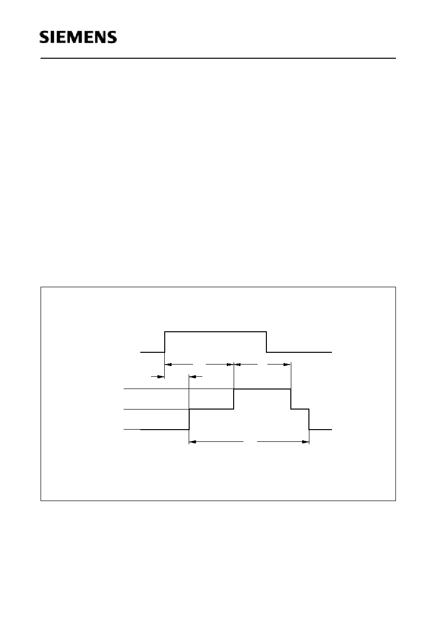
Figure 3
BG-pulse width
t
B
54 / CLL
Delay to HSYNC
t
DB
if CLEXT = L-level: (76-4
*
Internal-H-sync-phase) / CLL
if CLEXT = H-level:
(38-4
*
Internal-H-sync-phase) / CLL
UED10260
Input Signal
HSYNC
B
t
DB
t
DBL
t
t
BL
OH
V
OHBL
V
OL
V
SDA 9361
Semiconductor Group
12
1998-02-01
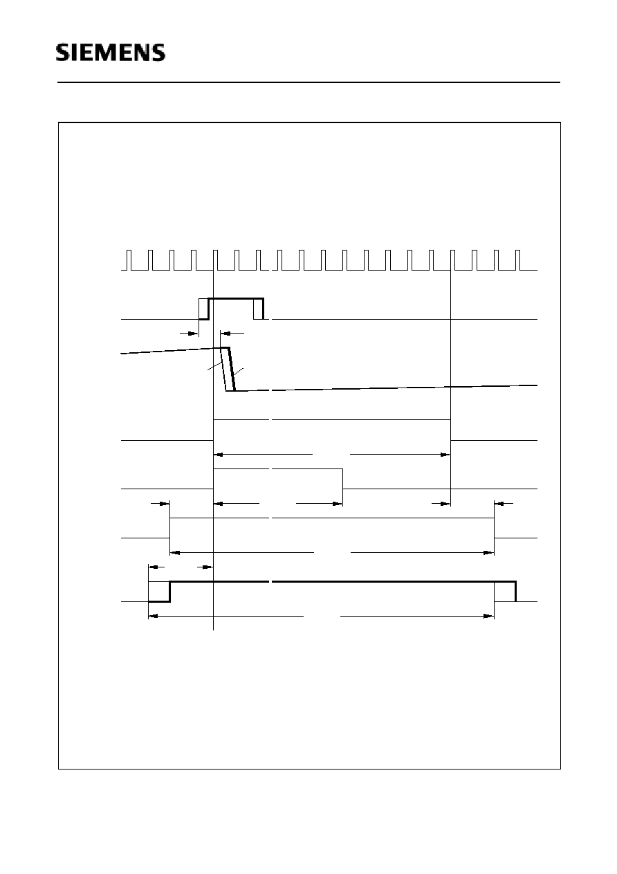
2.2
Circuit Description
The HSYNC is reference for a numeric PLL. This PLL generates a clock which is phase
locked to the incoming horizontal sync pulse and exactly 864 times faster then the
horizontal frequency. In order to lock the internal frequency to the external sync signal
positive horizontal sync pulses are required (see figure 4).
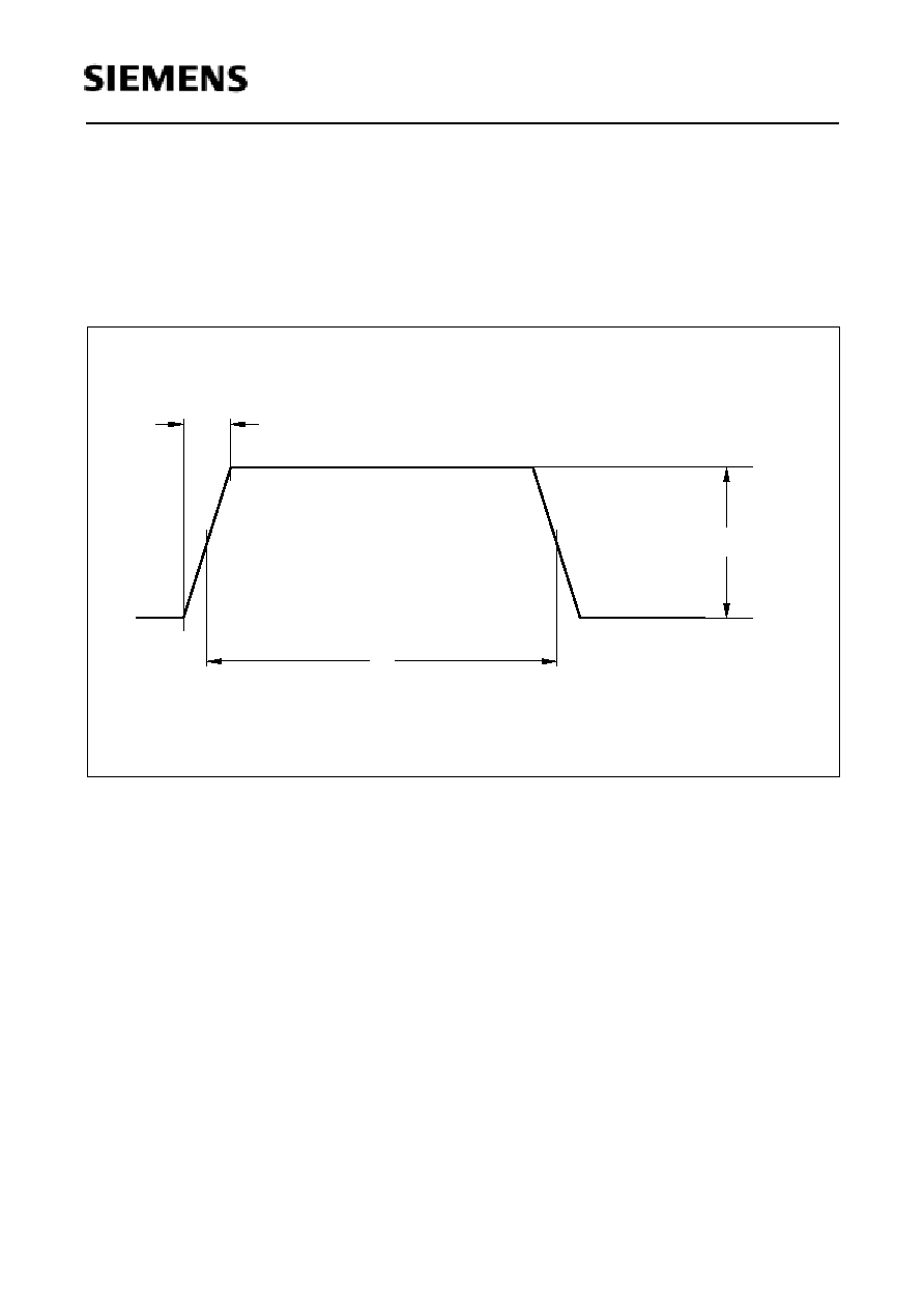
Figure 4
Incoming Signal HSYNC (CLEXT = 0)
Pulse width
t
w
for
2
C-Bus Bit 'HSWID' = 0:
3
µ
s ... 6.1
µ
s
low FH-range
1.5
µ
s ... 3.1
µ
s
high FH-range
Pulse width
t
w
for
2
C-Bus Bit 'HSWID' = 1:
3
µ
s ... 8.8
µ
s
low FH-range
1.5
µ
s ... 4.0
µ
s
high FH-range
Rise time
t
r
:100 ns minimum (CLEXT = 0)
The described input signal is first applied to an A/D converter. Conversion takes place
with 6 Bits and a nominal frequency of 27 MHz. The digital PLL uses a low pass filter to
obtain defined slopes for further measurements (PAL/NTSC applications). In addition
the actual high and low level of the signal as well as a threshold value is evaluated and
used to calculate the phase error between internal clock and external horizontal sync
UED10279
r
t
HSmax
V
HSmin
V
V
HSpp
W
t

SDA 9361
Semiconductor Group
13
1998-02-01
pulse. By means of digital PI filtering an increment is gained from this. The PI filter can
be set by the
2
C-Bus VCR bit so that the lock-in behavior of the PLL is optimal in relation
to either the TV or VCR mode. Moreover it is possible to adapt the nominal frequency by
means of 5
2
C-Bus bits (INCR4..INCR0) to different horizontal frequencies. An
additional bus bit GENMOD offers the possibility to use the PLL as a frequency
generator which frequency is controlled by the INCR bits.
Once an increment has been obtained, either from the PI-filter or the
2
C Bus, it can be
used to operate the Digital Timing Oscillator. The DTO generates a saw-tooth with a
frequency that is proportional to the increment. The saw-tooth is converted into a
sinusoidal clock signal by means of sin ROM's and D/A converters and applied to an
analog PLL which multiplies the frequency by 2 or 4 (depends on mode 1F
H
or 2F
H
; for
detailed explanation see pinning and
2
C-Bus description) and minimizes residual jitter.
In this manner the required line locked clock is provided to operate the other functional
parts of the circuit. If no HSYNC is applied to pin 35 the system holds its momentary
frequency for 2040 lines and following resets the PLL to its nominal frequency. The
status bit CON indicates the lock state of the PLL.
The system also provides a stable HS-pulse for internal use. The phase between this
internal pulse and the external HSYNC is adjustable via
2
C-Bus bits HPHASE. It can be
shifted over the range of one TV line.
An external clock (CLKI) can be provided by pin selection (CLEXT = H). The clock
frequency has to be 864
*
f
HSYNC
.
The external clock mode can not be used with
33.75 kHz and 35 kHz line frequency.
For effective noise suppression the VSYNC has to pass a window at first and is then
processed in a flywheel logic. The window allows a VSYNC pulse only after a minimum
number of lines from its predecessor and sets an artificial one after a maximum number
of lines. The number of H-periods between two subsequent VSYNCs is stored and
determines (after several checks) the following V-periods (internal synchronization). If
incoincidence is detected between internal and external VSYNC, the system switches
after a hysteresis of a defined number of V-periods to external synchronization and the
checks are repeated.
Values which influence shape and amplitude of the output signals are transmitted as
reduced binary values to the SDA 9361 via
2
C Bus. A CPU which is designed for speed
reasons in a pipe line structure calculates in consideration of feedback signals (e.g.ABL)
values which exactly represent the output signals. These values control after D/A
conversion the external deflection and raster correction circuits.
The CPU firmware is stored in an internal ROM.
SDA 9361
Semiconductor Group
14
1998-02-01
2.3
Reset Modes
The circuit is completely reset at power-on/off (timing diagram see figure 11) or if the
pin RESN has L-level (timing diagram see figure 12). During standby operation some
parts of the circuit are not affected (timing diagram see figure 12):
Note: Power-On-Reset and RESN = Low state are deactivated after ca. 32 cycles of the
X1/X2 oscillator clock and ca. 42 cycles of the CLL clock.
Standby state is deactivated after ca. 42 cycles of the CLL clock.
1)
Can only be read after Power-On-Reset is finished
Power-On-Reset
External Reset
(pin RESN = Low)
Standby Mode
(
I
2
C Bit STDBY = 1)
HD output
Low
Low
Active
H-protection
Inactive
Inactive
Inactive
V-protection
Inactive
Inactive
Inactive
2
C interface (SDA,
SCL)
Tristate
Tristate
Ready
2
C register
01
H
...1C
H
, 1F
H
Set to default values Set to default values Set to default values
2
C register 00
H
,
1D
H
, 1E
H
, 44
H
...48
H
Set to default values Set to default values Not affected
Status Bit PONRES
Set to 1
1)
Set to 1
1)
Not affected
V
REFP
,
V
REFH
.
V
REFL
Not affected
Not affected
Inactive
CPU
Inactive
Inactive
Inactive
SDA 9361
Semiconductor Group
15
1998-02-01
2.4
Frequency Ranges
The allowed deviation of all input line frequencies is max. ± 4.5 %.
n
L
:
number of lines per frame
I:
interlaced
NI:
non interlaced
If NSA = 0 (subaddress 01
H
/D5
H
) number of lines per field is selfadaptable between 192
and 680 for each specified H-frequency.
1)
Only with internal clock generation
H
V
n
L
15.625 kHz
50 Hz
625 I
15.75 kHz
60 Hz
525 I
31.25 kHz
50 Hz
100 Hz
625 NI / 1250I
625 I
31.5 kHz
60 Hz
70 Hz
120 Hz
525 NI / 1050 I
449 NI
525 I
32.4 kHz
60 Hz
1080 I
33.75 kHz
1)
60 Hz
1125 I
35 kHz
1)
66.7 Hz
525 NI
SDA 9361
Semiconductor Group
16
1998-02-01
2.5
I
2
C-Bus Control
2.5.1
I
2
C-Bus Address
2.5.2
I
2
C-Bus Format
write:
read:
Reading starts at the last write address n. Specification of a subaddress in reading mode
is not possible.
S:
Start condition
A:
Acknowledge
P:
Stop condition
NA:
Not Acknowledge
An automatically address increment function is implemented.
After switching on the IC, all bits are set to defined states.
1 0 0 0 1 1 0
S 1 0 0 0 1 1 0 0 A
Subaddress
A
Data Byte
A *****
A
P
S 1 0 0 0 1 1 0 1 A
Status byte
A
Data Byte n
A ***** NA P
SDA 9361
Semiconductor Group
17
1998-02-01
2.5.3
I
2
C-Bus Commands
1)
see 2.5.5: Explanation of some control items
Control item
Sub
-
add
r
. D7 D6 D5 D4 D3 D2 D1 D0 Allowed
Range
Effective
Range
Can be
Disabled
by Bit
Default
Value if
Disabled
Unit
Deflection control 0
00
H
see below
≠
≠
≠
≠
≠
Deflection control 1
01
H
see below
≠
≠
≠
≠
≠
Vertical shift
02
H
B7 B6 B5 B4 B3 B2 B1 B0 -128..127 -128..127
≠
≠
≠
Vertical size
03
H
B7 B6 B5 B4 B3 B2 B1 B0 -128..127 -128..127
≠
≠
≠
Vertical linearity
04
H
B7 B6 B5 B4 B3 B2 B1 B0 -128..127 -128..127
≠
≠
≠
Vertical S-correction
05
H
B7 B6 B5 B4 B3 B2 B1 B0 -128..127 -128..127
≠
≠
≠
Vertical EHT
compensation
1)
06
H
B7 B6 B5 B4 B3 B2 B1 B0
0..255
0..255
≠
≠
≠
Horizontal size
07
H
B7 B6 B5 B4 B3 B2 B1 B0 -128..127 -128..127
≠
≠
≠
Pin phase
08
H
B7 B6 B5 B4 B3 B2 B1 B0 -128..127 -128..127
≠
≠
≠
Pin amp
09
H
B7 B6 B5 B4 B3 B2 B1 B0 -128..127 -128..127
≠
≠
≠
Upper corner pin
correction
0A
H
B7 B6 B5 B4 B3 B2 B1 B0 -128..127 -128..127
≠
≠
≠
Lower corner pin
correction
0B
H
B7 B6 B5 B4 B3 B2 B1 B0 -128..127 -128..127
≠
≠
≠
Horizontal EHT
compensation
1)
0C
H
B7 B6 B5 B4 B3 B2 B1 B0
0..255
0..255
≠
≠
≠
Horizontal shift
0D
H
B6 B5 B4 B3 B2 B1 B0 X
-64..63
-64..63
≠
≠
1/CLL
Vertical angle
0E
H
B7 B6 B5 B4 B3 B2 B1 B0 -128..127 -128..127
≠
≠
≠
Vertical bow
0F
H
B7 B6 B5 B4 B3 B2 B1 B0 -128..127 -128..127
≠
≠
≠
PWM start
10
H
B7 B6 B5 B4 B3 B2 B1 B0
0..255
0..215
≠
≠
4/CLL
D/A
1)
11
H
B5 B4 B3 B2 B1 B0 X
X
-32..31
-32..31
≠
≠
≠
Vertical blanking time
1)
12
H
X B6 B5 B4 B3 B2 B1 B0
0..127
a)
BSE = 0
b)
lines
Horizontal blanking time 13
H
X
X
B5 B4 B3 B2 B1 B0
0..63
0..63
BSE = 0 H-flyback
4/CLL
Start vertical scan
1)
14
H
B7 B6 B5 B4 B3 B2 B1 B0 -128..127
c)
SSE = 0
9
line
Horizontal blanking
phase
15
H
B5 B4 B3 B2 B1 B0
-32..31
-32..31
≠
≠
4/CLL
Vertical scan width 0
1)
15
H
B9 B8
0..+3
d)
STE = 0
e)
256 lines
Vertical scan width 1
1)
16
H
B7 B6 B5 B4 B3 B2 B1 B0
0..255
d)
STE = 0
e)
lines
Guard band
1)
17
H
X
X
B5 B4 B3 B2 B1 B0
0..63
0..63
GBE = 0
3
half lines
Start reduced scan
1)
18
H
X
X
B5 B4 B3 B2 B1 B0
0..63
0, 2..63
SRSE =
0
2
line
Vertical sync control
19
H
see below
≠
≠
≠
≠
≠
Min. No. of lines / field
1)
1A
H
B7 B6 B5 B4 B3 B2 B1 B0
0..255
0..255
≠
≠
2 lines
Max. No. of lines / field
1)
1B
H
B7 B6 B5 B4 B3 B2 B1 B0
0..255
0..255
≠
≠
2 lines
AFC EHT
compensation
1)
1C
H
B5 B4 B3 B2 B1 B0 X
X
-32..31
-32..31
≠
≠
≠
Internal PLL control
1D
H
see below
≠
≠
≠
≠
≠
Internal H-sync phase
1E
H
B7 B6 B5 B4 B3 B2 B1 B0 -128..127 -96..119
≠
≠
4/CLL
PWM width
1F
H
B7 B6 B5 B4 B3 B2 B1 B0
0..255
0..215
PWM
width=0
15
4/CLL
Universal register 1
45
H
see below
≠
≠
≠
≠
≠
Universal register 3
47
H
see below
≠
≠
≠
≠
≠
Internal voltage Ref
control
48
H
see below
≠
≠
≠
≠
≠

SDA 9361
Semiconductor Group
18
1998-02-01
a) The effective range for Vertical Blanking Time:
16 ... 127 (absolute value)
if STE = 0
0 ... 127 (offset value)
if STE = 1.
b) The "default value if disabled" for Vertical Blanking Time:
21 (absolute value)if STE = 0
8 (offset value)if STE = 1.
c) The effective range for Start Vertical Scan:
2 ... 127 (absolute value)
if STE = 0
if STE = 1 and NSA = 1
-128 ... 127 (offset value)
if STE = 1 and NSA = 0.
d) The effective range for Vertical Scan (total width: 10 Bit): 160 ... 684 lines.
e) The "default value if disabled" for Vertical Scan equals the number of lines of the
source signal reduced by the control value for Start Vertical Scan. (E.g.: input signal:
262 lines per field; Start vertical scan = 8 lines; then (if SSE = 1, STE = 0) vertical
scan = 262 - 8 = 254 lines.
At power on the RAM containing the control items is cleared. Therefore all data are zero
by default (if not otherwise defined) before transferring individual values via
2
C Bus.
Allowed values out of the effective range are limited, e. g. Vertical blanking time = 3 is
limited to 16 if STE = 0 (that means a minimum of 16 lines is blanked).
There are five bits (SRSE, BSE, SSE, STE, GBE) in the deflection control byte 1 for
disabling some control items. If one of these bits is "0", the value of the corresponding
control item will be ignored and replaced by the value "default value if disabled" in the
table above.
2.5.4
Detailed Description
The Deflection Control Byte 0 includes the following bits:
VOFF:
Vertical off
0:
normal vertical output due to control items
1:
vertical saw-tooth is switched off,
vertical protection is disabled
Default value depends on pin 44 (VOFFD)
VOFFD = Low: 0
VOFFD = High: 1
VOFF
STDBY
2FH
BD
RABL
VR1
VR0
HDE

SDA 9361
Semiconductor Group
19
1998-02-01
STDBY:
Stand-by mode
0:
normal operation
1:
stand-by mode (all internal clocks are disabled)
2FH:
Setting of line frequency
0:
low range of line frequency (14900 Hz ... 17650 Hz)
1:
high range of line frequency (29800 Hz ... 35300 Hz)
Note: this bit is don't care if pin SELFH1_2 has L-level
BD:
Blanking disable
0:
horizontal and vertical blanking enabled
1:
horizontal and vertical blanking disabled
RABL:
ABL input range
0:
2 V ... 3 V
1:
0 V ... 4 V
VR1 ... VR0:
Reduction of the vertical size
00: 100 % V-size
(16:9 source on 16:9 display)
01: 75 % V-size
(16:9 source on 4:3 display)
10: 66 % V-size
(two 4:3 sources on 16:9 display)
11: 50 % V-size
(two 16:9 sources on 16:9 display)
HDE:
HD enable
0:
line is switched off (HD disabled, that is L-level)
1:
line is switched on (HD enabled)
Default value depends on pin 40 (SSD)
SSD = Low: 0
SSD = High: 1
The Deflection Control Byte 1 includes the following bits:
NSA:
No self adaptation
0:
self adaptation on
1:
self adaptation off
0
X
NSA
STE
GBE
SRSE
SSE
BSE

SDA 9361
Semiconductor Group
20
1998-02-01
STE:
Scan time enable
0:
control items for vertical scan width 0 and width 1 are disabled
1:
control items for vertical scan width 0 and width 1 are enabled
GBE:
Guard band enable
0:
control item for guard band is disabled
1:
control item for guard band is enabled
SRSE:
Start reduced scan enable
0:
control item for start reduced scan is disabled
1:
control item for start reduced scan is enabled
SSE:
Start scan enable
0:
control item for start vertical scan is disabled
1:
control item for start vertical scan is enabled
BSE:
Blanking select enable
0:
control items for blanking times are disabled
1:
control items for blanking times are enabled
The Vertical Sync Control Byte includes the following bits:
SSC:
Sandcastle without VBL
0:
output SCP with VBL component
1:
output SCP without VBL component
NR:
Noise reduction
0:
no noise reduction of the vertical sync
1:
noise reduction of the vertical sync
NI:
Non interlace
0:
interlace depends on source
1:
no interlace
X
X
SSC
NR
NI
NL2
NL1
NL0
SDA 9361
Semiconductor Group
21
1998-02-01
NL2 ... NL0:
Number of lines per field when NR = 1 and no vertical sync
at the input is detected
The Internal PLL Control Byte includes the following bits:
HSWID:
Maximum width of HSYNC
0:
6.1
µ
s
for low FH-range
3.1
µ
s
for high FH-range
1:
8.8
µ
s
for low FH-range
4.0
µ
s
for high FH-range
GENMOD:
Clock generator mode
0:
normal PLL mode
1:
generator mode (fixed frequency output, controlled by INCR..)
VCR:
PLL filter optimized for
0:
TV mode
1:
VCR mode
INCR4 ... 0:
Nominal PLL output frequency
for low FH-range:
INCR = INT((FH
*
110592) / FQ - 64.625)
for high FH-range:
INCR = INT((FH
*
55296) / FQ - 64.625)
(for typical values see table below)
NL2
NL1
NL0
Number of Lines per Field
0
0
0
262.5
0
0
1
312.5
0
1
0
525
0
1
1
562.5
1
X
X
625
HSWID
GENMOD
VCR
INCR4
INCR3
INCR2
INCR1
INCR0
SDA 9361
Semiconductor Group
22
1998-02-01
specified range for:
GENMOD = 0:
6
INCR
14
GENMOD = 1:
3
INCR
18
(FQ = 24.576 MHz)
Default value: INCR = 6
Warning:
1)A change of INCR or 2FH causes spontaneous changes of the generated clock
frequency greater than the specified 4.5 %.
Switching from PLL mode to Generator mode (GENMOD) with constant INCR
values does not result in exceeding the specified frequency deviation range.
2)If pin SSD has H-level the output signal HD starts immediately after power on. In
this case the starting horizontal frequency is either 15.75 kHz (if SELFH1_2 has
H-level or if SELFH1_2 and FH1_2 have L-level) or 31.5 kHz (if SELFH1_2 has
L-level and FH1_2 H-level). Starting with Muse or Macintosh standard requires
L-level at SSD so that INCR can be changed before enabling HD with HDE = 1.
3)Using external clock at pin 1, CLKI, (pin 32, CLEXT = 1): no internal protection
against missing clock pulses is provided.
4)In order to guarantee error free operation of the build in soft start circuit the input
frequency has to be inside the lock range of the PLL (+/-4.5 % of standard input
frequency)
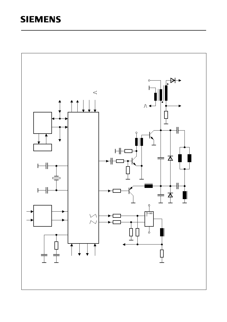
Application
FH[Hz]
INCR
PAL
15625
6
NTSC
15750
6
PAL (100 Hz)
31250
6
NTSC (120 Hz)
31500
6
ATV
32400
8
MUSE
33750
11
Macintosh
35000
14
SDA 9361
Semiconductor Group
23
1998-02-01
The Universal Register 1 (Subaddress 45
H
) includes the following bit:
NOISYVCR:
Handling of noisy input signals in VCR mode
0:
normal handling
1:
improved handling
Note: this bit is don't care if bit VCR = 0 (TV mode)
The Universal Register 3 (Subaddress 47
H
) includes the following bits:
KILL_ZIP:
Top flutter suppression
0:
no top flutter suppression
1: top
flutter
suppression
(phase jumps max.
±
12
µ
s for low FH-range
rsp. max.
±
6
µ
s for high FH-range)
TC_3RD:
Third time constant
0:
slow VCR time constant
1:
fast VCR time constant
Note: this bit is don't care if bit VCR = 0 (TV mode)
The Internal Voltage Ref. Control Byte includes the following bits:
BANDG4 ...
Adjustment of internal bandgap reference
BANDG0:
10000: Reference Output voltage min
:
01111: Reference Output voltage max
Typical adjustment range is 0.5 V.
BANDGOFF: Bandgap Off
0:
V
REFH
,
V
REFL
derived internally from
V
REFP
0
0
NOISY
VCR
0
0
0
0
0
0
0
0
KILL_ZIP TC_3RD
0
0
0
BANDG4 BANDG3 BANDG2 BANDG1 BANDG0
BANDG
OFF
BANDG4
OFF
0
SDA 9361
Semiconductor Group
24
1998-02-01
1:
external references on
V
REFP
,
V
REFH
,
V
REFL
have to be applied
(in this case BANDG4OFF must be = 1)
BANDG4OFF: Bandgap 4 V Off
0:
internal bandgap reference is used for
V
REFP
1:
external reference on
V
REFP
(4 V) has to be applied
The Status Byte includes the following bits:
HPON:
protection on
0:
normal operation of the line output stage
1:
high level on input HPROT has switched off the line
VPON:
V-protection on
0:
normal operation of the vertical output stage
1:
incorrect signal on input VPROT has switched off the line
CON:
Coincidence not
0:
H-coincidence detected
1:
no H-coincidence detected
PONRES:
Power-On-Reset
0:
after bus master has read the status byte
1:
after each detected reset
Note: PONRES is reset after this byte has been read.
2.5.5
Explanation of Some Control Items
D/A
This item controls directly a 6 Bit D/A Converter at the output D/A that can be used for
general purpose.
Start Vertical Scan
If enabled (SSE = 1) this control item defines the start of calculation of the vertical saw-
tooth, the east/west parabola and the vertical function required for the vertical modulated
output HD.
HPON
VPON
CON
-
-
-
-
PONRES

SDA 9361
Semiconductor Group
25
1998-02-01
Vertical Scan (width0 and width1)
The total width of this control item is 10 Bit. Therefore two registers (width0 and width1)
are necessary. If enabled (STE = 1) it defines the duration of the vertical scan. When the
vertical period has more lines than the sum of Start Vertical Scan and Vertical Scan,
the calculation of the vertical saw-tooth, the east/west parabola and the vertical parabola
required for HD stops so that the corresponding output signals remain unchanged till the
next vertical synchron pulse.
Guard Band
This control item is useful for optimizing self adaptation. Video signals with different
number of lines in consecutive fields (e. g. VCR search mode) must not start the
procedure of self adaptation. But switching between different TV standards has to
change the slope of the vertical saw-tooth getting always the same amplitude (self
adaptation). To avoid problems with flicker free TV systems which have alternating
number of lines per field an average value of four consecutive fields is calculated. If the
deviation of these average values (e.g. PAL: 312.5 lines or 625 half lines) is less or
equals Guard Band, no adaptation takes place. When it exceeds Guard Band, the
vertical slope will be changed.
Start Reduced Scan
If enabled (SRSE = 1) this item defines the start of the D/A conversion of the calculated
vertical saw-tooth. From begin of the vertical flyback to the line defined by Start
Reduced Scan the output signals VD+, VD- remain unchanged (flyback level). Other
outputs are not affected.
a) control bits VR1, VR0 # 00 (reduction of vertical size)
In this case the byte is useful for e.g. displaying 16/9 source format on 4/3 picture
tubes without visible RGB lines generated of the automatic cut-off control (partial
overscan). It defines the start of the reduced amplitude (factors 0.5, 0.66, 0.75) of the
vertical saw-tooth (refer page 39). When Start Reduced Scan = 0 the reduction
takes place over all lines including vertical flyback.
b) control bits VR1, VR0 = 00 (no reduction of vertical size)
If Start Reduced Scan > Start Vertical Scan the D/A conversion of the saw-tooth
starts (Start Reduced Scan - Start Vertical Scan) lines after begin of the
calculation. This causes a jump of the output voltage VD+, VD- from flyback to scan
level. It may be useful to hide the automatic cut-off control lines if no overscan is
desired (e.g. for VGA display). If Start Reduced Scan <= Start Vertical Scan this
byte has no effect.

SDA 9361
Semiconductor Group
26
1998-02-01
Vertical EHT Compensation
This item controls the influence of the beam current dependent input signal ABL on the
outputs VD+ and VD- according to the following equation:
(if RABL = 0)
(if RABL = 1)
V
VDPP
: variation of VD+ and VD- peak-to-peak voltage
V
ABL
: variation of ABL input voltage
1)
The factor 0.57 depends on
V
REFP
,
V
REFH
,
V
REFL
If Vertical EHT Compensation = 0 the outputs VD+ and VD- are independent of
the input signal ABL.
Horizontal EHT Compensation
This item controls the influence of the input signal ABL on the output E/W according to
the following equation:
(if RABL = 0)
(if RABL = 1)
V
EW
: variation of E/W output voltage
V
ABL
: variation of ABL input voltage
1)
The factor 2.12 depends on
V
REFP
,
V
REFH
,
V
REFL
If Horizontal EHT Compensation = 0 the output E/W is independent of the input
signal ABL.
AFC EHT Compensation
Deviation of the horizontal phase caused by high beam current (e.g. white bar) can be
eliminated by this control item. The beam current dependent input signal ABL is
multiplied by AFC EHT Compensation.
V
VDPP
V
ABL
*
Vertical EHT compensation
512
------------------------------------------------------------------------ * 0,57
1
)
=
V
VDPP
V
ABL
*
Vertical EHT compensation
2048
------------------------------------------------------------------------ * 0,57
1
)
=
V
EW
V
ABL
*
Horizontal EHT compensation
128
---------------------------------------------------------------------------------- * 2,12
1
)
=
V
EW
V
ABL
*
Horizontal EHT compensation
512
---------------------------------------------------------------------------------- * 2,12
1
)
=

SDA 9361
Semiconductor Group
27
1998-02-01
Additional to the control items Vertical angle, Vertical bow and Horizontal shift, this
product influences the horizontal phase at the output HD according to the following
equation:
(if RABL = 0)
(if RABL = 1)
:variation of horizontal phase at the output HD
(positive values: shift left, negatives values: shift right)
V
ABL
:variation of ABL input voltage (units: Volt)
CLL
:864
*
F
H
1)
The factor 52 depends on
V
REFP
Vertical Blanking Time (VBT)
VBT defines the vertical blanking pulse VBL which is part of the output signal SCP. VBL
is synchronized with the leading edge of HSYNC. It always starts and stops at the
beginning of line and never in the center.
a) Case of STE = 0
In this case the control item Vertical blanking time defines the duration of the
V-blanking pulse (VBL) exactly in number of lines. Because of IC internal limitations
16 through 127 lines can be blanked. If BSE = 0 the control item Vertical blanking
time is disabled and always 21 lines (default value if disabled) are blanked.
After power on the control bit BSE is 0. Therefore 21 lines will be blanked before any
programming of the IC. If Vertical Blanking Time is less or equals 21 lines, VBL
starts (point A in fig. above) always 0 ... 0.5 line (new odd field) or 0.5 ... 1 line (new
even field) prior to the vertical flyback. Otherwise VBL is concentric to a fictitious
vertical flyback period of 21 lines, that means VBL starts (VBT - 21) / 2 lines at the
end of an odd field or (VBT - 20) / 2 at the end of an even field prior to point A.
Possible start points are only the beginning of line.
V
ABL
*
AFC EHT compensation
64
---------------------------------------------------------------- *
52
1
)
CLL
-----------
=
V
ABL
*
AFC EHT compensation
256
---------------------------------------------------------------- *
52
1
)
CLL
-----------
=
SDA 9361
Semiconductor Group
28
1998-02-01
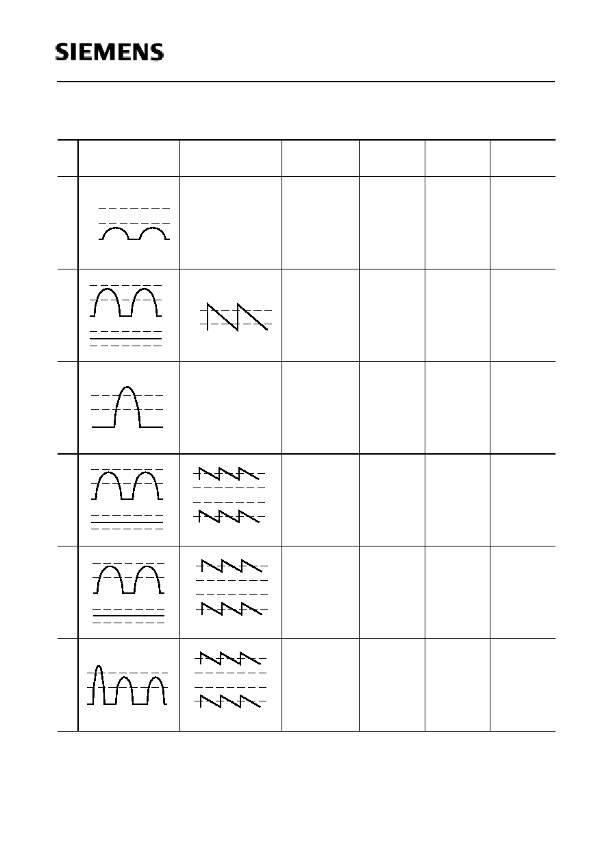
Figure 5
Vertical Blanking Pulse VBL when STE = 0 and Number of Lines per
UED10261
1
~ ~
2
14
15
16
17
18
19
20
21
22
23
24
25
HSYNC
~ ~
VSYNC
VD-
VBL
(BSE = 0)
(BSE = 1,
VBL
VBT = 16)
(BSE = 1,
VBT = 25)
VBL
VBT = 26)
(BSE = 1,
VBL
1 Line
Start of even Field
Start of odd Field
21 Lines
16 Lines
2 Lines
25 Lines
3 Lines
26 Lines
A
~~
~~
~~
~~
~~
2 Lines
SDA 9361
Semiconductor Group
29
1998-02-01
Field = Constant
b) Case of STE = 1
In this case the control item Vertical blanking time is an extension for the V-blanking
pulse.
- If BSE = 1 and VBT = 0 the V-blanking pulse has its minimum: it starts always at
end of scan (line B in Fig. below) and ends at start of scan (line C) defined by the
control items Start Vertical Scan (if SSE = 1) and Vertical Scan.
- BSE = 1 and (128 > VBT > 0) extend the V-blanking pulse according to the following
relationship
(If VBT > 127 this value is ignored and replaced by VBT - 128):
VBL starts VBT / 2 lines (even field) respectively (VBT + 1) / 2 lines (odd field)
prior to line B.
VBL ends (VBT + 1) / 2 lines (even field) respectively VBT / 2 lines (odd field) after
end of line C.
Possible start points are only the beginning of line.
- If BSE = 0 (after power on) the control item Vertical Blanking Time is disabled and
VBL starts 4 lines prior to end of scan (line B) and ends 4 lines after start of scan
(line C).
Figure 6
Vertical Blanking Pulse VBL when STE = 1
UED10262
~ ~
B
1
2
3
C
HSYNC
~ ~
VSYNC
VD-
VBL
(BSE = 0)
(BSE = 1,
VBL
VBT = 0)
VBT = 7)
(BSE = 1,
VBL
1 Line
Start of even Field
Start of odd Field
3 Lines
~~
~~
~~
~~
~ ~
~~
~ ~
~ ~
~ ~
4 Lines
3 Lines
4 Lines
Even
B
C
SDA 9361
Semiconductor Group
30
1998-02-01
Minimum Number of Lines per Field
It defines the minimum number of lines per field for the vertical synchronisation. If the TV
standard at the inputs VSYNC and HSYNC has less lines per field than defined by
Minimum Number of Lines per Field no synchronisation is possible.The relationship
between Minimum Number of Lines per Field
and the minimum number of lines is
given in the following table:
Maximum Number of Lines per Field
It defines the maximum number of lines per field for the vertical synchronisation. If the
TV standard at the inputs VSYNC and HSYNC has more lines per field than defined by
Maximum Number of Lines per Field no synchronisation is possible. The relationship
between Maximum Number of Lines per Field and the maximum number of lines is
given in the following table:
Minimum Number of Lines per Field
Minimum Number of Lines per Field
0
192
1
194
...
...
127
446
128
448
...
...
254
700
255
702
Maximum Number of Lines per Field
Maximum Number of Lines per Field
0
702
1
192
2
194
...
...
127
444
128
446
...
...
255
700
SDA 9361
Semiconductor Group
31
1998-02-01
Most Important V-Deflection Modes for 4:3 CRT
Mode
Description
Characteristics
Notes
VR1
VR0
NSA SRSE GBE STE SSE
N0 Normal mode
(for 4:3 source,
Letterbox)
with default
settings
Self adaptation
scan start = line 9
start of V-ramp = line 9
scan time: depends on source signal
guard band = 1.5 lines
Mode after
power on
00
0
0
0
0
0
N1 Normal mode
(for 4:3 source,
Letterbox)
with user
defined values
Self adaptation
scan start = Start Vertical Scan
if (Start Reduced Scan>Start Vertical Scan)
start of V-ramp = Start Reduced Scan
else
start of V-ramp = Start Vertical Scan
scan time: depends on source signal
guard band = Guard Band/2 [lines]
Start of scan
adjustable
start of
V-ramp
adjustable
guard band
adjustable
00
0
1
1
0
1
S0 Shrink
mode 75%
(for 16:9 source)
with default
settings
Self adaptation
scan start = line 9
start of reduced V-ramp = line 9
scan time: depends on source signal
guard band = 1.5 lines
01
0
0
0
0
0
S1 Shrink
mode 75%
(for 16:9 source)
with user
defined values
Self adaptation
scan start = Start Vertical Scan
if (Start Reduced Scan>Start Vertical Scan)
start of reduced V-ramp =
Start Reduced Scan
else
start of reduced V-ramp =
Start Vertical Scan
scan time: depends on source signal
guard band = Guard Band/2 [lines]
Start of scan
adjustable
start of
reduced
V-ramp
adjustable
guard band
adjustable
01
0
1
1
0
1
SDA 9361
Semiconductor Group
32
1998-02-01
Most Important V-Deflection Modes for 16:9 CRT
Mode
Description
Characteristics
Notes
VR1
VR0
NSA SRSE GBE STE SSE
N0 Normal mode
(for 16:9 or
4:3 source)
with default
settings
Self adaptation
scan start = line 9
start of V-ramp = line 9
scan time: depends on source signal
guard band = 1.5 lines
Mode after
power on
00
0
0
0
0
0
N1 Normal mode
(for 16:9 or
4:3 source)
with user
defined values
Self adaptation
scan start = Start Vertical Scan
if (Start Reduced Scan>Start Vertical Scan)
start of V-ramp = Start Reduced Scan
else
start of V-ramp = Start Vertical Scan
scan time: depends on source signal
guard band = Guard Band/2 [lines]
Start of scan
adjustable
start of
V-ramp
adjustable
guard band
adjustable
00
0
1
1
0
1
Z
Zoom mode
(for 4:3 source,
Letterbox)
scan start =
(number_of_lines - Vertical Scan)/2 + 8
scan time = Vertical Scan
Vertical
scan
controls
zoom factor
00
0
X
X
1
0
SC Scroll mode
(for 4:3 source,
Letterbox)
Scan start =
(number_of_lines - Vertical Scan)/2 + 8
+ Start Vertical Scan
scan time = Vertical Scan
Like above;
Start vertical
scan can be
additionally
used for
adjustment
of picture
phase
00
0
X
X
1
1
M
Manual mode
(for 4:3 source,
Letterbox)
Scan start = Start Vertical Scan
scan time = Vertical Scan
Scan start
and
scan time
are
separately
adjustable
00
1
X
X
1
X
S2 Shrink
mode 66%
(for two
4:3 sources)
with default
settings
Self adaptation
scan start = line 9
start of reduced V-ramp = line 9
scan time: depends on source signal
guard band =1.5 lines
10
0
0
0
0
0
S3 Shrink
mode 50%
(for two
16:9 sources)
with default
settings
Self adaptation
scan start = line 9
start of reduced V-ramp = line 9
scan time: depends on source signal
guard band = 1.5 lines
11
0
0
0
0
0
SDA 9361
Semiconductor Group
33
1998-02-01
3
Absolute Maximum Ratings
Note: Absolute Maximum Ratings are those values beyond which damage to the device
may occur. Functional operation under these conditions or at any other condition
beyond those indicated in the operational sections of this specification is
not implied.
1)
Between any internally non-connected supply pin of the same kind.
All
V
DD(D)
- and
V
DD(A)
- Pins are connected internally by about 3
The
V
SS(D)
-Pins are connected internally by about 3
Parameter
Symbol
Limit Values
Unit
Remark
min.
max.
Operating temperature
T
A
-20
70
∞C
Storage temperature
T
stg
-40
125
∞C
Junction temperature
T
j
125
∞C
Soldering temperature
T
S
260
∞C
Input voltage
V
I
V
SS
- 0.3 V
V
DD
+ 0.3 V
Output voltage
V
Q
V
SS
- 0.3 V
V
DD
+ 0.3 V
Supply voltages
V
DD
-0.3
6
V
Supply total voltage
differentials
-0.25
0.25
V
1)
Total power dissipation
P
tot
0.85
W
Latch-up protection
-100
100
mA
All inputs/outputs
SDA 9361
Semiconductor Group
34
1998-02-01
3.1
Recommended Operating Conditions
Parameter
Symbol
Limit Values
Unit
Remark
min.
nom.
max.
Supply voltages
V
DD
4.5
5
5.5
V
Ambient temperature
T
A
-20
25
70
∞C
For analog
parameters: 0∞C
TTL Inputs: CLKI, VSYNC, TEST, FH1_2, SELFH1_2, CLEXT, SSD, VOFFD, RESN
H-input voltage
V
IH
2.0
V
DD
V
L-input voltage
V
IL
0
0.8
V
Input VPROT
Threshold V1
1.4
1.5
1.6
V
V
REFP
= 4 V
Threshold V2
0.9
1.0
1.1
V
V
REFP
= 4 V
Input HPROT
Threshold V1
3.9
4
4.1
V
V
REFP
= 4 V
Threshold V2
2.1
2.4
2.7
V
V
REFP
= 4 V
Input ABL
L-input voltage
V
IL
2
V
V
REFP
= 4 V
RABL = 0
0
V
V
REFP
= 4 V RABL = 1
Full range input
voltage
3
V
V
REFP
= 4 V
RABL = 0
4
V
V
REFP
= 4 V RABL = 1
Reference Voltage Input Pins (Internal Voltage Ref. Control Byte Reg 48H = 00000110)
V
REFP
input voltage
V
VREFP
4
V
V
REFH
input voltage
V
VREFH
2.5
V
V
REFL
input voltage
V
VREFL
1.2
V
V
REFN
input voltage
V
VREFN
0
V
V
REFC
input voltage
V
VREFC
5
V
Independent of
register 48
H
,
max =
V
DD
SDA 9361
Semiconductor Group
35
1998-02-01
3.1
Recommended Operating Conditions (cont'd)
Parameter
Symbol
Limit Values
Unit
Remark
min.
nom.
max.
Input
2
L-input voltage
V
IL
0
0.7
V
V
REFP
= 4 V
H-input voltage
V
IH
2.0
V
DD
V
V
REFP
= 4 V
Input HSYNC (CLEXT = 0)
Input voltage range
V
HSpp
2
V
DD
V
See page 12
Input voltage low level
V
HSmin
0
V
See page 12
Input voltage high level
V
HSmax
V
DD
See page 12
Pulse width
(HSWID = 0)
t
w
3.0
6.1
µ
s
Low FH-range
1.5
3.1
µ
s
High FH-range
Pulse width
(HSWID = 1)
t
w
3.0
8.8
µ
s
Low FH-range
1.5
4.0
µs
High FH-range
Rise time
t
r
100
ns
Input HSYNC (CLEXT = 1)
L-input voltage
V
IL
0
0.8
V
H-input voltage
V
IH
2.0
V
DD
V
Setup time
t
SU
4
ns
Referred to falling
edge of CLKI
Hold time
t
H
12
ns
Referred to falling
edge of CLKI
Input VSYNC
Pulse width high
100
100/
f
H
ns
FH1_2 = 1, NI = 0
Pulse width high
200
100/
f
H
ns
FH1_2 = 0, NI = 0
Pulse width high
1.5/
f
H
100/
f
H
NI = 1
SDA 9361
Semiconductor Group
36
1998-02-01
3.1
Recommended Operating Conditions (cont'd)
Parameter
Symbol
Limit Values
Unit
Remark
min.
nom.
max.
Input CLKI (External Clock Generation, CLEXT = High)
Input frequency
f
I
12.5
13.5
15
MHz
Low FH-range
25
27
30
MHz
High FH-range
Quartz Oscillator Input / Output X1, X2
Crystal frequency
24.576
MHz
Fundamental
crystal type,
e.g. Saronix
9922 520 00282
Crystal resonant
impedance
40
External capacitance
27
pF
See Application
information
I
2
C Bus (All Values are Referred to min.(
V
IH
) and max.(
V
IL
)
High-level input
voltage
V
IH
3
V
DD
V
Low-level input
voltage
V
IL
0
1.5
V
SCLK clock frequency
f
SCLK
0
400
kHz
Rise times of SCLK,
SDAT
t
R
0.3
µ
s
f
SCLK
= 400 kHz
Fall times of SCLK,
SDAT
t
F
0.3
µ
s
Set-up time DATA
t
SU;DAT
100
ns
Hold time DATA
t
HD;DAT
0
ns
Load capacitance
C
L
400
pF
SDA 9361
Semiconductor Group
37
1998-02-01
3.2
Characteristics (Assuming Recommended Operating Conditions)
Parameter
Symbol
Limit Values
Unit
Remark
min.
nom.
max.
Average supply
current
I
CC
90
150
mA
Stand-by supply
current
25
mA
Output Pins: SCAN, PWM
Output low level
V
OL
0.4
V
I
O
= 1 mA
Output high level
V
OH
2.8
V
I
O
= -1 mA
Input / Output SDAT
Output low level
V
OL
0.6
V
I
O
= 6 mA
Output SCP
Output low level
V
OL
0
1
V
I
O
= 1 mA
Output HBL level
V
OHBL
V
DD
/ 2
-0.4 V
V
DD
/ 2
V
DD
/ 2
+0.4 V
|
I
O
| = 100
µ
A
Output high level
V
OH
4.0
V
DD
V
I
O
= -1 mA
DAC Output D/A
DAC resolution
6
Bit
DAC output low
1
V
V
REFP
= 4 V
DAC output high
3.953
V
V
REFP
= 4 V
Load capacitance
C
L
30
pF
Output load
20
k
Offset error
-3 %
3 %
V
REFP
= 4 V
Gain error
-3 %
3 %
V
REFP
= 4 V
INL
-1
1
LSB
DNL
-0.5
0.5
LSB
DAC Output E/W
DAC resolution
10
Bit
Linear range:
100 ... 900
DAC output low
1.45
V
Input data = 100
1)
SDA 9361
Semiconductor Group
38
1998-02-01
3.2
Characteristics (Assuming Recommended Operating Conditions)
(cont'd)
Parameter
Symbol
Limit Values
Unit
Remark
min.
nom.
max.
DAC output high
3.48
V
Input data = 900
1)
Load capacitance
C
L
30
pF
Output load
20
k
Zero error
-2 %
2 %
DAC output
voltage = 2.5 V
2)
Gain error
-5 %
5 %
2)
INL
-0.2 %
0.2 %
2)
DNL
-0.1 %
0.1 %
2)
1)
V
REFH
= 2.5 V,
V
REFL
= 1.2 V
2)
V
REFH
= 2.5 V,
V
REFL
= 1.2 V, Input range = 100 ... 900
DAC Output VD+, VD-
DAC resolution
14
Bit
Linear range:
1500 ... 15000
DAC output low (VD-)
1.44
V
Input data = 1500
1)
DAC output high (VD-)
3.58
V
Input data = 15000
1)
DAC output low
(VD-) - (VD+)
-2.12
V
Input data = 1500
1)
DAC output high
(VD-) - (VD+)
2.16
V
Input data = 15000
1)
Load capacitance
C
L
30
pF
Output load
20
k
Zero error
-1 %
1 %
(VD-) - (VD+) = 0 V
2)
Gain error
-5 %
5 %
2)
INL
-0.5 %
0.5 %
2)
DNL
Monotonous
Guaranteed by design
1)
V
REFH
= 2.5 V,
V
REFL
= 1.2 V
2)
V
REFH
= 2.5 V,
V
REFL
= 1.2 V, Input range = 1500 ... 15000
SDA 9361
Semiconductor Group
39
1998-02-01
3.2
Characteristics (Assuming Recommended Operating Conditions)
(cont'd)
Parameter
Symbol
Limit Values
Unit
Remark
min.
nom.
max.
Reference Output
V
REFP
(Adjustable by Reg 48
H
, Bit D7 ... D3)
(
Reg 48
H
, Bit D2 = 0, Bit D1 = 0)
Output voltage min
4.0
V
Bit D7 ... D3 = 10000
Output voltage max
4.0
V
Bit D7 ... D3 = 01111
Output current
I
Q
-50
0
µ
A
Reference Output
V
REFH
(Reg 48
H
, Bit D2 = 0)
Output voltage
V
Q
2.4
2.5
2.6
V
V
REFP
= 4 V
Reference Output
V
REFL
(Reg 48
H
, Bit D2 = 0)
Output voltage
V
Q
1.1
1.2
1.3
V
V
REFP
= 4 V
Output HD
Output low level
V
OL
0
1
V
I
O
= 8 mA
Output high level
V
OH
V
DD
-1 V
V
DD
I
O
= -8 mA
SDA 9361
Semiconductor Group
40
1998-02-01
4
Application Information
Figure 7
UES10280
Source Sel
Synch Sep
NVM
TV Contr.
SDA 9361
2
C
24.576
MHz
27 pF
27 pF
X1
X2
VSYNC
HSYNC
LF
+
H-Coil
V
B
EHT
ABL
HD
E/W
+
V-Coil
VPROT
VD-
VD+
SCP
SCAN
VPROT
HPROT
2
+
_
RESN
PWM
D/A
ABL

SDA 9361
Semiconductor Group
41
1998-02-01
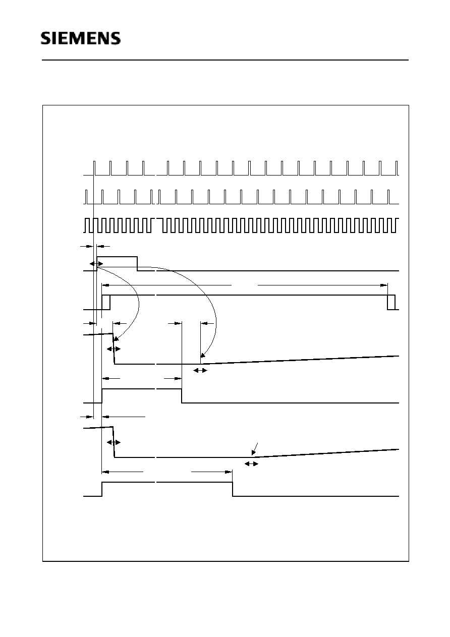
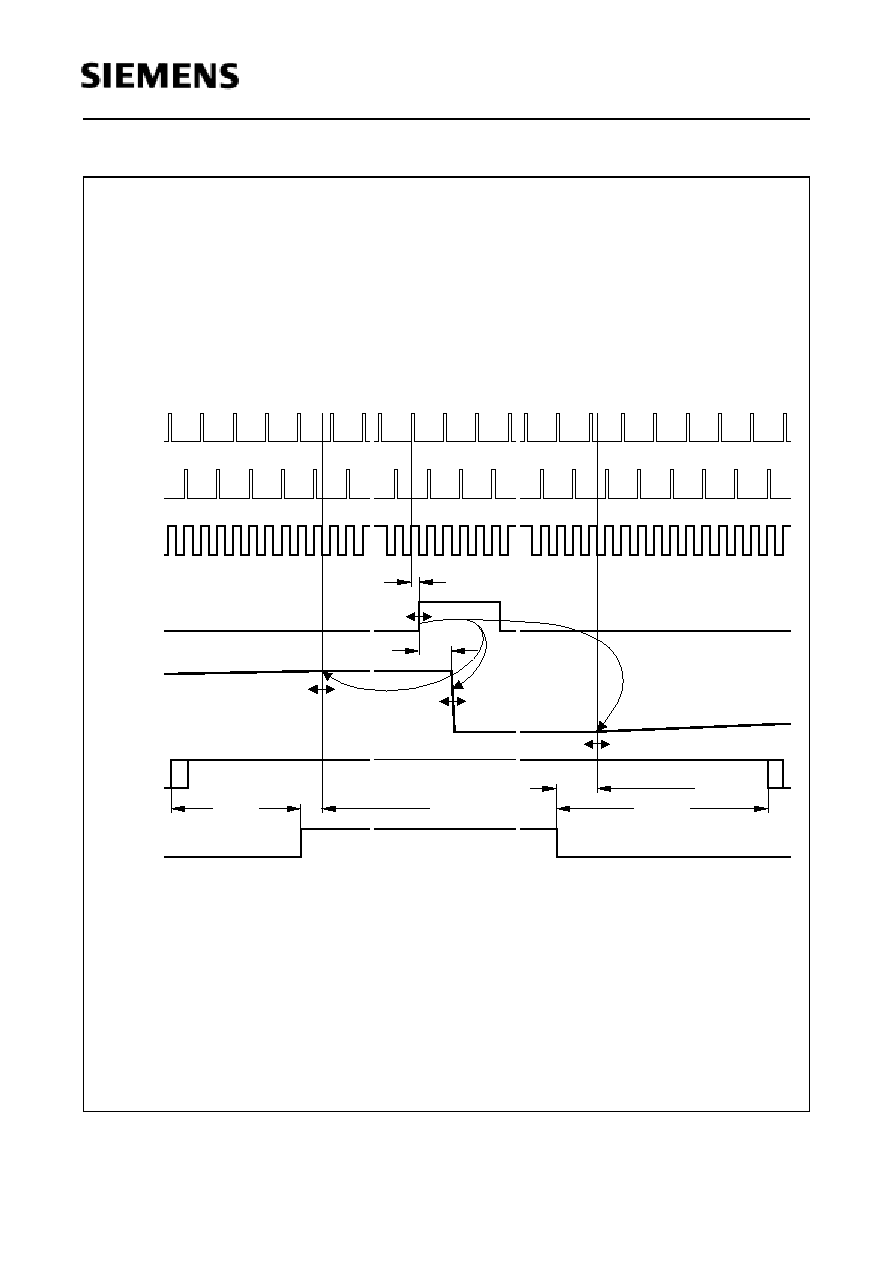
5
Waveforms
5.1
VD- Output Voltage, 4/3-CRT and 16/9-Source
Figure 8
UED10264
VD-
V
0(max)
V
0(min)
V
(Line No.)
z
n
SRS
2
63
0
1
2
V
V
16/9
2
1
4/3 =
V
V
2
1
V
V 16/9
0.75
SRSE = 1
Start Reduced Scan (SRS) selectable (line 0, 2...63)
SDA 9361
Semiconductor Group
42
1998-02-01
5.2
Timing Diagram of SCAN
Figure 9
Timing Diagram of SCAN if STE = 0
UED10281
1
2
3
8
~ ~
~~
9
10
11
12
13
14
15
16
17
18
19
20
21
22
3
2
1
8
9
10
11
12
13
14
15
16
17
18
19
20
21
22
~~
~ ~
HSYNC
(odd field)
(even field)
HSYNC
d0
2
(internal)
*FH
VSYNC
~ ~
21 Lines
VBL
(BSE = 0)
1 Line
(SSE = 0)
VD-
~ ~
~~
(SSE = 0)
SCAN
appr. 8.5 Lines
(SSE = 1,
VD-
~ ~
appr. 0.5 Lines
scan = 12)
start vert.
appr. 11.5 Lines
(SSE = 1,
SCAN
~ ~
start vert.
scan = 12)
Start of Scan
appr. 1 Line + d0
Start of Scan
SDA 9361
Semiconductor Group
43
1998-02-01
Figure 10
Timing Diagram of SCAN if STE = 1
UED10282
1
2
3
~ ~
~~
3
2
1
~~
~ ~
HSYNC
(odd field)
(even field)
HSYNC
d0
2
(internal)
*FH
VSYNC
~ ~
VBL
(BSE = 0)
1 Line
VD-
~ ~
appr. 0.5 Line + d0
SCAN
~ ~
~ ~
~~
~ ~
~ ~
End of Scan
~ ~
Start of Scan
~ ~
~ ~
4 Lines
5.5 Lines
appr. 1 Line + d0
SDA 9361
Semiconductor Group
44
1998-02-01
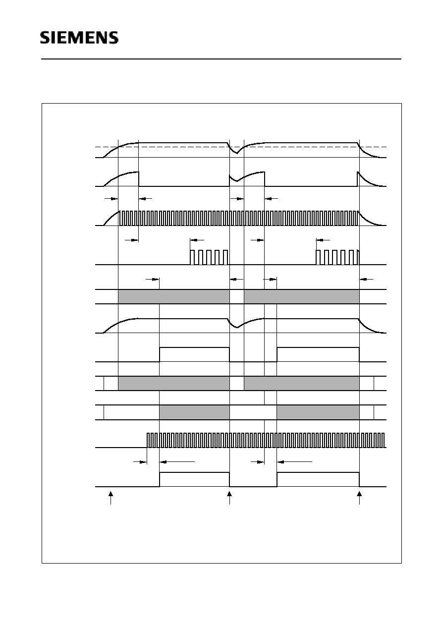
5.3
Power On/Off Diagram
Figure 11
UED10283
,
V
REFH
Programmable
~ 42 Cycles
For low FH-range this time has to be multiplied by 2
Power On
1)
Default
C Reg.
Active
Inactive
CPU
H
CLL
01
H
1C
...
H
1F
,
Active
Inactive
,
44
48
2
H
...
C Reg.
00
H
2
1D
,
H
H
1E ,
H
Protection
REFL
V
De-
fault
Glitch
Power Off
Programmable
~ 42 Cycles
Default
Programmable
De-
fault
Programmable
fault
De-
fault
De-
SSD = 1: ~ 380
SSD = 0: ~ 250
C Registers 01
Tristate
REFP
V
,
C Bus
2
HD
2
X1, X2
On-
Reset
Power-
Cycles
32
Voltage
Supply
SSD = 1: ~ 380
SSD = 0: ~ 250
µ
s
1)
1F
Programmable
Ready
1C
...
H
,
H
Tri-
state
H
1)
µ
s
Cycles
32
s
µ
1)
H
Programmable
Ready
C Registers 01
2
H
1C
...
Tristate
H
,1F
s
µ
1)
SDA 9361
Semiconductor Group
45
1998-02-01
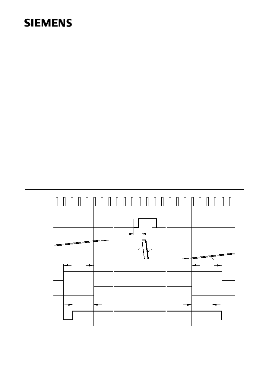
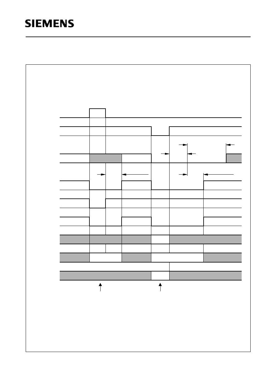
5.4
Standby Mode, RESN Diagram
Figure 12
UED10284
Active
REFL
Ready
Default Values
Programmable
Standby Mode
For low FH-range this time has to be multiplied by 2
1)
1E
H
H
,
H
,
...
44
H
48
C Reg.
00
2
1D
H
Inactive
Programmable
2
C Bus
C Reg.
...
01
H
2
1C
H
1F
,
H
Protection
Default Values
External Reset
Values
Default
Programmable
Tristate
Programmable
Programmable
Ready
Free Run
HD
2-Loop
Active
Inactive
Active
Inactive
CPU
V
REFP
REFH
V
V
,
,
RESN
Standby
32 x 1
Cycles
2-Loop
~ 42 CLL Cycles
Run
~ 42 CLL Cycles
SSD = 0: ~ 250
SSD = 1: ~ 380
µ
µ
1)
s
Free
1)
s
SDA 9361
Semiconductor Group
46
1998-02-01
5.5
Function of H,V Protection
t
0
= 2 /
f
v
... 3 /
f
v
t
1
= 64 /
f
v
... 128 /
f
v
t
2
= 1 /
f
v
... 2 /
f
v
1)
Depends on
2
C-control items
2)
HPON or VPON = 1:HD = 0 (OFF)
HPROT
VPROT
Mode
SCP
HPON
2)
I
2
C Bus
VPON
2)
I
2
C Bus
1
Start up
Continuous
blanking
0
0
2
H, V
operation
1)
0
0
3
EHT over-
voltage
Continuous
blanking
after
t
2
1
after
t
2
0
4
H operation
V short
failure
Continuous
blanking
after
t
0
if
SSC = 0
0
0
5
V longer
failure
H off
after
t
1
Continuous
blanking
after
t
0
if
SSC = 0
0
1
after
t
1
6
EHT
short over-
voltage
Continuous
blanking
after
t
2
1
after
t
2
1
after
t
1
V1
V2
or
V1
V2
or
or
0
t
1
t
t
_
<
<
or
or
1
t
t <
or
1
t
t <
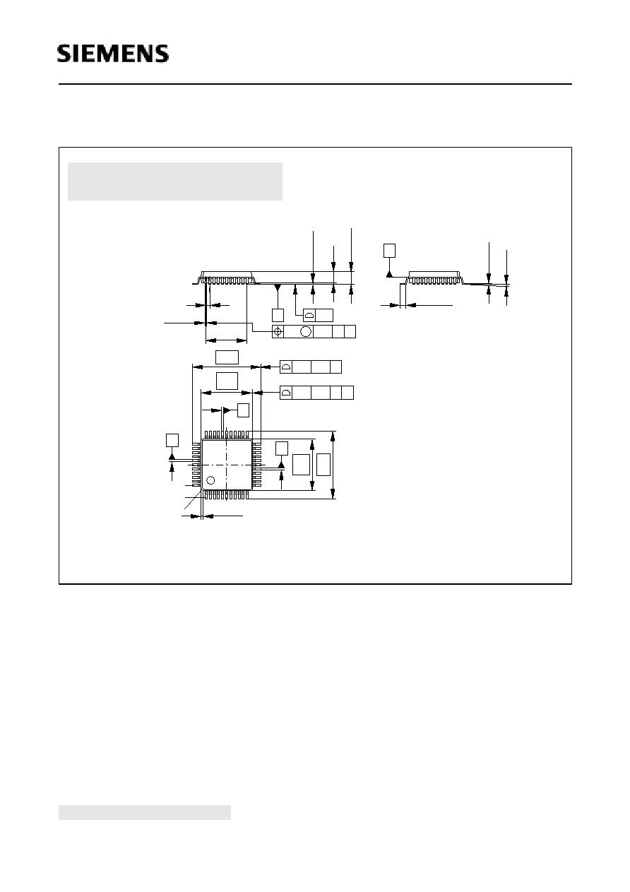
SDA 9361
Semiconductor Group
47
1998-02-01
6
Package Outlines
Figure 13
Index Marking
Does not include plastic or metal protrusions of 0.25 max per side
GPM05622
0.8
0.3 +0.15
8
C
0.1
0.2
M
A-B D C 44x
0.25 min.
2
+0.1
-0.05
2.45 max.
D
10
1)
D
A-B
0.2
H 4x
13.2
D
A-B
0.2
44x
B
1)
10
13.2
A
44
1
0.6 x 45∞
H
0.88 ±0.15
+0.08
-0.02
0.15
7∞ max.
1)
P-MQFP-44-2
(Plastic Metric Quad Flat Package)
Sorts of Packing
Package outlines for tubes, trays etc. are contained in our
Data Book "Package Information".
SMD = Surface Mounted Device
Dimensions in mm