 | –≠–ª–µ–∫—Ç—Ä–æ–Ω–Ω—ã–π –∫–æ–º–ø–æ–Ω–µ–Ω—Ç: SPB46N03 | –°–∫–∞—á–∞—Ç—å:  PDF PDF  ZIP ZIP |
1
Semiconductor Group
SPP46N03
SIPMOS
Æ
Power Transistor
Product Summary
Drain source voltage
30
V
DS
V
Drain-Source on-state resistance
0.015
R
DS(on)
I
D
Continuous drain current
46
A
Features
∑
N channel
∑
Enhancement mode
∑
Avalanche rated
∑
d
v
/d
t
rated
∑
175∞C operating temperature
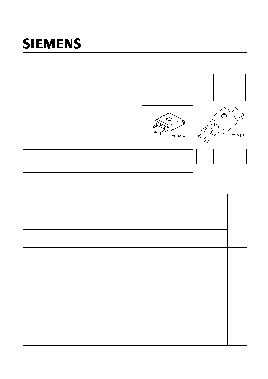
Pin 1
Pin 2
Pin 3
G
D
S
Packaging
Type
Package
Ordering Code
SPP46N03
Tube
P-TO220-3-1 Q67040-S4742-A2
SPB46N03
Tape and Reel
Q67040-S4145-A3
P-TO263-3-2
Maximum Ratings, at
Tj = 25 ∞C, unless otherwise specified
Parameter
Symbol
Unit
Value
Continuous drain current
T
C
= 25 ∞C,
1)
T
C
= 100 ∞C
46
46
I
D
A
Pulsed drain current
T
C
= 25 ∞C
I
Dpulse
184
Avalanche energy, single pulse
I
D
= 46 A,
V
DD
= 25 V,
R
GS
= 25
mJ
E
AS
250
Avalanche energy, periodic limited by
T
jmax
12
E
AR
Reverse diode d
v/dt
I
S
= 46 A,
V
DS
= 24 V, d
i/dt = 200 A/µs,
T
jmax
= 175 ∞C
d
v/dt
6
kV/µs
Gate source voltage
V
GS
±
20
V
Power dissipation
T
C
= 25 ∞C
P
tot
120
W
Operating and storage temperature
T
j ,
T
stg
∞C
-55... +175
55/175/56
IEC climatic category; DIN IEC 68-1
2
Semiconductor Group
SPP46N03
Thermal Characteristics
Parameter
Values
Symbol
Unit
typ.
max.
min.
Characteristics
R
thJC
-
1.25
K/W
Thermal resistance, junction - case
-
Thermal resistance, junction - ambient, leded
R
thJA
-
62
-
-
-
-
62
40
SMD version, device on PCB:
@ min. footprint
@ 6 cm
2
cooling area
2)
R
thJA
Electrical Characteristics, at
Tj = 25 ∞C, unless otherwise specified
Parameter
Symbol
Unit
Values
min.
max.
typ.
Static Characteristics
Drain- source breakdown voltage
V
GS
= 0 V,
I
D
= 0.25 mA
-
V
(BR)DSS
30
-
V
Gate threshold voltage,
V
GS
=
V
DS
I
D
= 80 µA
V
GS(th)
4
3
2.1
Zero gate voltage drain current
V
DS
= 30 V,
V
GS
= 0 V,
T
j
= 25 ∞C
V
DS
= 30 V,
V
GS
= 0 V,
T
j
= 150 ∞C
-
I
DSS
µA
1
100
0.1
-
Gate-source leakage current
V
GS
= 20 V,
V
DS
= 0 V
I
GSS
-
10
nA
100
Drain-Source on-state resistance
V
GS
= 10 V,
I
D
= 46 A
R
DS(on)
-
0.009
0.015
1current limited by bond wire
2 Device on 40mm*40mm*1.5mm epoxy PCB FR4 with 6 cm2 (one layer, 70µm thick) copper area for drain
connection. PCB is vertical without blown air.
3
Semiconductor Group
SPP46N03
Electrical Characteristics, at
Tj = 25 ∞C, unless otherwise specified
Parameter
Symbol
Values
Unit
min.
typ.
max.
Dynamic Characteristics
Transconductance
V
DS
2*
I
D
*
R
DS(on)max
,
I
D
= 46 A
g
fs
20
39
-
S
Input capacitance
V
GS
= 0 V,
V
DS
= 25 V,
f = 1 MHz
C
iss
-
1400
1750
pF
Output capacitance
V
GS
= 0 V,
V
DS
= 25 V,
f = 1 MHz
C
oss
-
645
810
Reverse transfer capacitance
V
GS
= 0 V,
V
DS
= 25 V,
f = 1 MHz
C
rss
-
260
325
Turn-on delay time
V
DD
= 15 V,
V
GS
= 10 V,
I
D
= 46 A,
R
G
= 6.8
t
d(on)
-
13
20
ns
Rise time
V
DD
= 15 V,
V
GS
= 10 V,
I
D
= 46 A,
R
G
= 6.8
t
r
-
24
36
Turn-off delay time
V
DD
= 15 V,
V
GS
= 10 V,
I
D
= 46 A,
R
G
= 6.8
t
d(off)
-
27
42
Fall time
V
DD
= 15 V,
V
GS
= 10 V,
I
D
= 46 A,
R
G
= 6.8
t
f
-
24
36
4
Semiconductor Group
SPP46N03
Electrical Characteristics, at
Tj = 25 ∞C, unless otherwise specified
Parameter
Symbol
Values
Unit
min.
typ.
max.
Dynamic Characteristics
Gate to source charge
V
DD
= 24 V,
I
D
= 46 A
11
nC
7
Q
gs
-
-
19
Q
gd
Gate to drain charge
V
DD
= 24 V,
I
D
= 46 A
28.5
Gate charge total
V
DD
= 24 V,
I
D
= 46 A,
V
GS
= 0 to 10 V
-
39
60
Q
g
Gate plateau voltage
V
DD
= 24 V,
I
D
= 46 A
V
(plateau)
5.5
-
V
-
Reverse Diode
Inverse diode continuous forward current
T
C
= 25 ∞C
I
S
-
-
46
A
Inverse diode direct current,pulsed
T
C
= 25 ∞C
I
SM
-
-
184
Inverse diode forward voltage
V
GS
= 0 V,
I
F
= 92 A
V
SD
-
1.06
V
1.7
Reverse recovery time
V
R
= 15 V,
I
F
=
I
S
, d
i
F
/d
t = 100 A/µs
t
rr
-
40
ns
60
Reverse recovery charge
V
R
= 15 V,
I
F=
l
S
, d
i
F
/d
t = 100 A/µs
Q
rr
-
µC
0.04
0.06
5
Semiconductor Group
SPP46N03
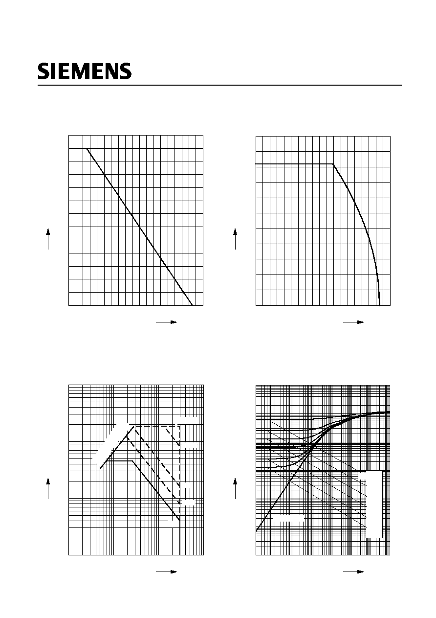
Power Dissipation
P
tot
=
f (T
C
)
0
20
40
60
80
100 120 140 160 ∞C 190
T
C
0
10
20
30
40
50
60
70
80
90
100
110
W
130
SPP46N03
P
tot
Drain current
I
D
=
f (T
C
)
parameter:
V
GS
10 V
0
20
40
60
80
100 120 140 160 ∞C 190
T
C
0
5
10
15
20
25
30
35
40
45
A
55
SPP46N03
I
D
Transient thermal impedance
Z
thJC
=
f (t
p
)
parameter :
D = t
p
/
T
10
-7
10
-6
10
-5
10
-4
10
-3
10
-2
10
0
s
t
p
-5
10
-4
10
-3
10
-2
10
-1
10
0
10
1
10
K/W
SPP46N03
Z
thJC
single pulse
0.01
0.02
0.05
0.10
0.20
D = 0.50
Safe operating area
I
D
=
f (V
DS
)
parameter :
D = 0 , T
C
= 25 ∞C
10
-1
10
0
10
1
10
2
V
V
DS
0
10
1
10
2
10
3
10
A
SPP46N03
I
D
R
D
S
(o
n)
=
V
DS
/
I
D
DC
10 ms
1 ms
100 µs
t
p
= 41.0µs
6
Semiconductor Group
SPP46N03
Typ. output characteristics
I
D
=
f (V
DS
)
parameter:
t
p
= 80 µs
0.0
0.5 1.0
1.5 2.0
2.5 3.0
3.5 4.0
V
5.0
V
DS
0
10
20
30
40
50
60
70
80
90
100
A
120
SPP46N03
I
D
V
GS
[V]
a
a
4.0
b
b
4.5
c
c
5.0
d
d
5.5
e
e
6.0
f
f
6.5
g
g
7.0
h
h
7.5
i
i
8.0
j
j
9.0
k
k
10.0
l
P
tot
= 120W
l
20.0
Typ. drain-source-on-resistance
R
DS(on)
=
f (I
D
)
parameter:
V
GS
0
10
20
30
40
50
60
70
A
85
I
D
0.000
0.005
0.010
0.015
0.020
0.025
0.030
0.035
0.040
0.050
SPP46N03
R
DS(on)
V
GS
[V] =
b
b
4.5
c
c
5.0
d
d
5.5
e
e
6.0
f
f
6.5
g
g
7.0
h
h
7.5
i
i
8.0
j
j
9.0
k
k
10.0
l
l
20.0
Typ. transfer characteristics
I
D
=
f (V
GS
)
parameter:
t
p
= 80 µs
V
DS
2 x
I
D
x
R
DS(on)max
2.8
3.2
3.8
4.2
4.8
5.2
V
6.0
V
GS
0
5
10
15
20
25
30
35
40
45
50
55
60
A
70
I
D
Typ. forward transconductance
g
fs
= f(I
D
)
; T
j
= 25∞C
parameter:
g
fs
0
10
20
30
40
A
60
I
D
0
5
10
15
20
25
30
35
S
45
g
fs
7
Semiconductor Group
SPP46N03
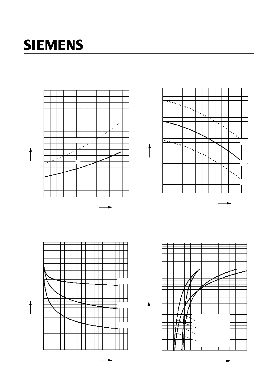
Drain-source on-resistance
R
DS(on)
=
f (T
j
)
parameter :
I
D
= 46 A,
V
GS
= 10 V
-60
-20
20
60
100
140
∞C
200
T
j
0.000
0.004
0.008
0.012
0.016
0.020
0.024
0.028
0.036
SPP46N03
R
DS(on)
typ
98%
Gate threshold voltage
V
GS(th)
=
f (T
j
)
parameter :
V
GS
=
V
DS
,
I
D
= 80 µA
-60
-20
20
60
100
140
∞C
200
T
j
0.0
0.4
0.8
1.2
1.6
2.0
2.4
2.8
3.2
3.6
4.0
4.4
V
5.0
V
GS(th)
min
typ
max
Typ. capacitances
C =
f (V
DS
)
parameter:
V
GS
= 0 V,
f = 1 MHz
0
4
8
12
16
20
24
28
32
V
40
V
DS
2
10
3
10
4
10
pF
C
0
4
8
12
16
20
24
28
32
V
40
V
DS
2
10
3
10
4
10
pF
C
Ciss
Coss
Crss
Forward characteristics of reverse diode
I
F
=
f (V
SD
)
parameter:
T
j
,
t
p
= 80 µs
0.0
0.4
0.8
1.2
1.6
2.0
2.4
V
3.0
V
SD
0
10
1
10
2
10
3
10
A
SPP46N03
I
F
T
j
= 25 ∞C typ
T
j
= 25 ∞C (98%)
T
j
= 175 ∞C typ
T
j
= 175 ∞C (98%)

8
Semiconductor Group
SPP46N03
Typ. gate charge
V
GS
=
f (Q
Gate
)
parameter:
I
D puls
= 46 A
0
10
20
30
40
nC
60
Q
Gate
0
2
4
6
8
10
12
V
16
SPP46N03
V
GS
DS max
V
0,8
DS max
V
0,2
Avalanche Energy
E
AS
=
f (T
j
)
parameter:
I
D
= 46 A,
V
DD
= 25 V
R
GS
= 25
20
40
60
80
100
120
140
∞C
180
T
j
0
50
100
150
mJ
250
E
AS
Drain-source breakdown voltage
V
(BR)DSS
=
f (T
j
)
-60
-20
20
60
100
140
∞C
200
T
j
27
28
29
30
31
32
33
34
35
V
37
SPP46N03
V
(BR)DSS

9
Semiconductor Group
SPP46N03
Edition 02 / 1999
Published by Siemens AG,
Bereich Halbleiter Vetrieb,
Werbung, Balanstraþe 73,
81541 M¸nchen
© Siemens AG 1997
All Rights Reserved.
Attention please!
As far as patents or other rights of third parties are concerned, liability is only assumed for components,
not for applications, processes and circuits implemented within components or assemblies.
The information describes a type of component and shall not be considered as warranted characteristics.
Terms of delivery and rights to change design reserved.
For questions on technology, delivery and prices please contact the Semiconductor Group Offices in Germany
or the Siemens Companies and Representatives worldwide (see address list).
Due to technical requirements components may contain dangerous substances. For information on the types
in question please contact your nearest Siemens Office, Semiconductor Group.
Siemens AG is an approved CECC manufacturer.
Packing
Please use the recycling operators known to you. We can also help you - get in touch with your nearest sales
office. By agreement we will take packing material back, if it is sorted. You must bear the costs of transport.
For packing material that is returned to us unsorted or which we are not obliged to accept, we shall have to
invoice you for any costs incurred.
Components used in life-support devices or systems must be expressly authorized for such purpose!
Critical components
1
of the Semiconductor Group of Siemens AG, may only be used in life-support devices or
systems
2
with the express written approval of the Semiconductor Group of Siemens AG.
1)A critical component is a component used in a life-support device or system whose failure can reasonably be
expected to cause the failure of that life-support device or system, or to affect its safety or effectiveness of
that device or system.
2)Life support devices or systems are intended (a) to be implanted in the human body, or (b) to support and/or
maintain and sustain and/or protecf human life. If they fail, it is reasonable to assume that the health of the
user or other persons may be endangered.