 | –≠–ª–µ–∫—Ç—Ä–æ–Ω–Ω—ã–π –∫–æ–º–ø–æ–Ω–µ–Ω—Ç: SPU28N05L | –°–∫–∞—á–∞—Ç—å:  PDF PDF  ZIP ZIP |
Semiconductor Group
1
30/Jan/1998
SPD28N05L
SPU28N05L
SIPMOS
Æ
Power Transistor
∑ N channel
∑ Enhancement mode
∑ Logic Level
∑ Avalanche-rated
∑ dv/dt rated
∑ 175∞C operating temperature
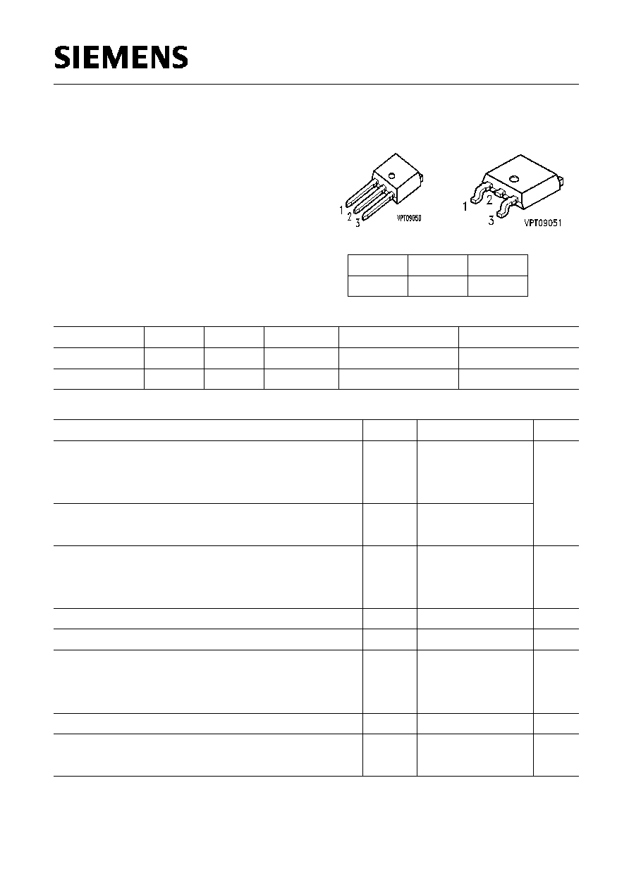
Pin 1
Pin 2
Pin 3
G
D
S
Type
V
DS
I
D
R
DS(on)
Package
Ordering Code
SPD28N05L
55 V
28 A
0.05
P-TO252
Q67040 - S4122 - A2
SPU28N05L
55 V
28 A
0.05
P-TO251
Q67040 - S4114 - A2
Maximum Ratings
Parameter
Symbol
Values
Unit
Continuous drain current
T
C
= 25 ∞C
T
C
= 100 ∞C
I
D
20
28
A
Pulsed drain current
T
C
= 25 ∞C
I
Dpuls
112
Avalanche energy, single pulse
I
D
= 28 A, V
DD
= 25 V, R
GS
= 25
L = 357 µH, T
j
= 25 ∞C
E
AS
140
mJ
Avalanche current,limited by T
jmax
I
AR
28
A
Avalanche energy,periodic limited by T
jmax
E
AR
7.5
mJ
Reverse diode dv/dt
I
S
= 30 A, V
DS
= 40 V, di
F
/dt = 200 A/µs
T
jmax
= 175 ∞C
dv/dt
6
kV/µs
Gate source voltage
V
GS
±
14
V
Power dissipation
T
C
= 25 ∞C
P
tot
75
W
Semiconductor Group
2
30/Jan/1998
SPD28N05L
SPU28N05L
Maximum Ratings
Parameter
Symbol
Values
Unit
Operating temperature
T
j
-55 ... + 175
∞C
Storage temperature
T
stg
-55 ... + 175
Thermal resistance, junction - case
R
thJC
2
K/W
Thermal resistance, junction - ambient (PCB mount)**
R
thJA
50
Thermal resistance, junction - ambient
R
thJA
100
IEC climatic category, DIN IEC 68-1
55 / 175 / 56
** when mounted on 1 " square PCB ( FR4 );for recommended footprint
Electrical Characteristics,
at T
j
= 25∞C, unless otherwise specified
Parameter
Symbol
Values
Unit
min.
typ.
max.
Static Characteristics
Drain- source breakdown voltage
V
GS
= 0 V, I
D
= 0.25 mA, T
j
= 25 ∞C
V
(BR)DSS
55
-
-
V
Gate threshold voltage
V
GS=
V
DS,
I
D
= 50 µA
V
GS(th)
1.2
1.6
2
Zero gate voltage drain current
V
DS
= 50 V, V
GS
= 0 V, T
j
= -40 ∞C
V
DS
= 50 V, V
GS
= 0 V, T
j
= 25 ∞C
V
DS
= 50 V, V
GS
= 0 V, T
j
= 150 ∞C
I
DSS
-
-
-
-
0.1
-
100
1
0.1
µA
Gate-source leakage current
V
GS
= 20 V, V
DS
= 0 V
I
GSS
-
10
100
nA
Drain-Source on-resistance
V
GS
= 4.5 V, I
D
= 20 A
V
GS
= 10 V, I
D
= 20 A
R
DS(on)
-
-
0.025
0.04
0.03
0.05

Semiconductor Group
3
30/Jan/1998
SPD28N05L
SPU28N05L
Electrical Characteristics,
at T
j
= 25∞C, unless otherwise specified
Parameter
Symbol
Values
Unit
min.
typ.
max.
Dynamic Characteristics
Transconductance
V
DS
2
*
I
D *
R
DS(on)max,
I
D
= 20 A
g
fs
10
20
-
S
Input capacitance
V
GS
= 0 V, V
DS
= 25 V, f = 1 MHz
C
iss
-
770
960
pF
Output capacitance
V
GS
= 0 V, V
DS
= 25 V, f = 1 MHz
C
oss
-
230
300
Reverse transfer capacitance
V
GS
= 0 V, V
DS
= 25 V, f = 1 MHz
C
rss
-
130
165
Turn-on delay time
V
DD
= 30 V, V
GS
= 4.5 V, I
D
= 28 A
R
G
= 6.8
t
d(on)
-
10
15
ns
Rise time
V
DD
= 30 V, V
GS
= 4.5 V, I
D
= 28 A
R
G
= 6.8
t
r
-
75
115
Turn-off delay time
V
DD
= 30 V, V
GS
= 4.5 V, I
D
= 28 A
R
G
= 6.8
t
d(off)
-
30
45
Fall time
V
DD
= 30 V, V
GS
= 4.5 V, I
D
= 28 A
R
G
= 6.8
t
f
-
20
30
Gate charge at threshold
V
DD
= 40 V, I
D
0.1 A, V
GS
=0 to 1 V
Q
g(th)
-
1
1.5
nC
Gate charge at 5.0 V
V
DD
= 40 V, I
D
= 28 A, V
GS
=0 to 5 V
Q
g(5)
-
20
30
Gate charge total
V
DD
= 40 V, I
D
= 28 A, V
GS
=0 to 10 V
Q
g(total)
-
32
50
Gate plateau voltage
V
DD
= 40 V, I
D
= 28 A
V
(plateau)
-
4
-
V
Semiconductor Group
4
30/Jan/1998
SPD28N05L
SPU28N05L
Electrical Characteristics,
at T
j
= 25∞C, unless otherwise specified
Parameter
Symbol
Values
Unit
min.
typ.
max.
Reverse Diode
Inverse diode continuous forward current
T
C
= 25 ∞C
I
S
-
-
28
A
Inverse diode direct current,pulsed
T
C
= 25 ∞C
I
SM
-
-
112
Inverse diode forward voltage
V
GS
= 0 V, I
F
= 56 A
V
SD
-
1.1
1.8
V
Reverse recovery time
V
R
= 30 V, I
F=
l
S,
di
F
/dt = 100 A/µs
t
rr
-
60
90
ns
Reverse recovery charge
V
R
= 30 V, I
F=
l
S,
di
F
/dt = 100 A/µs
Q
rr
-
0.15
0.25
µC
Semiconductor Group
5
30/Jan/1998
SPD28N05L
SPU28N05L
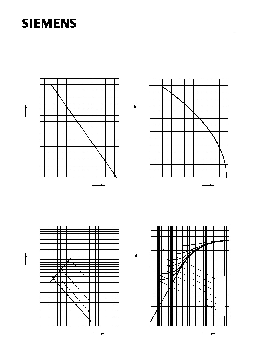
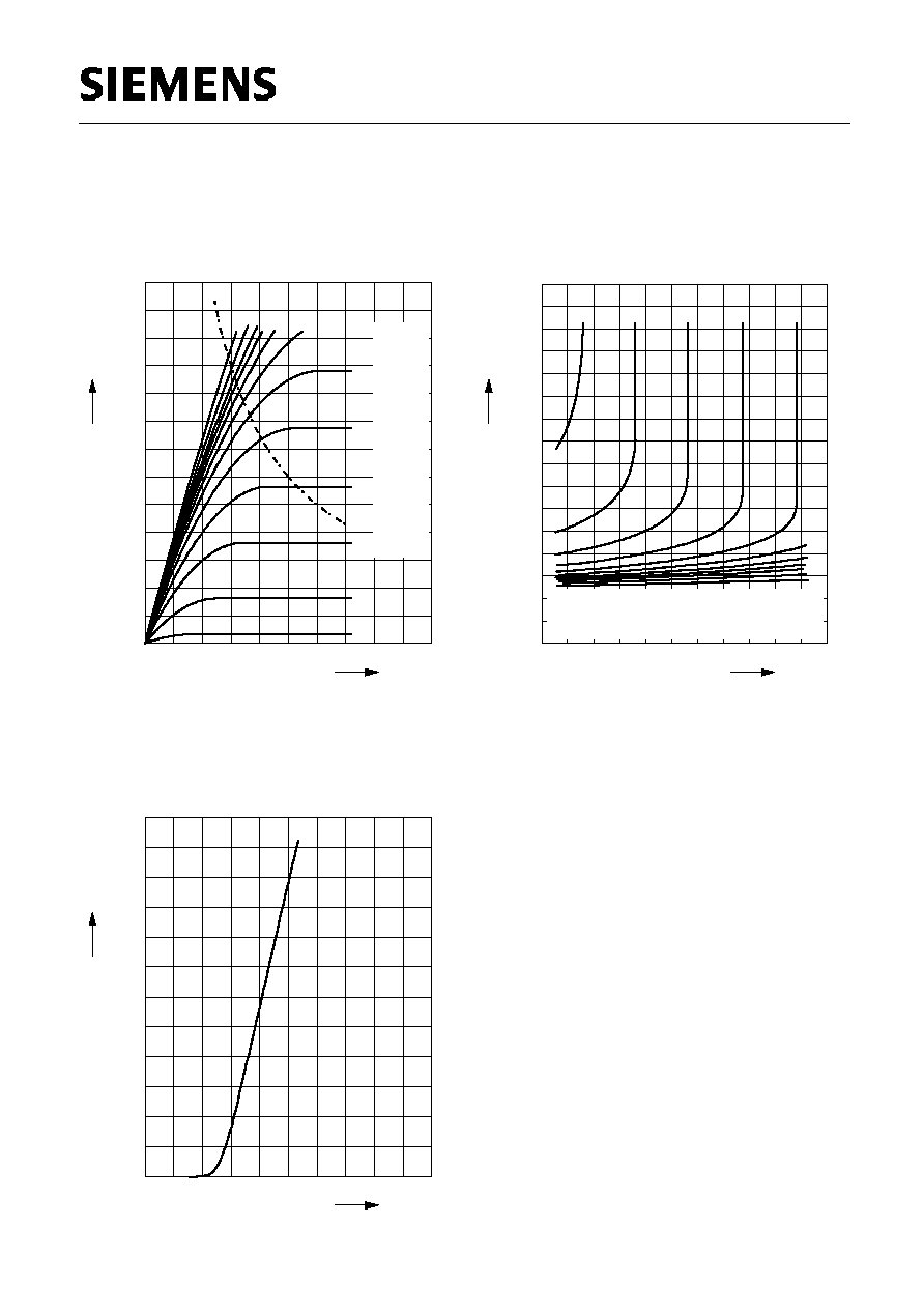
Power dissipation
P
tot
=
(
T
C
)
0
20
40
60
80
100
120
140
∞C
180
T
C
0
10
20
30
40
50
60
W
80
P
tot
Drain current
I
D
=
(
T
C
)
parameter:
V
GS
4 V
0
20
40
60
80
100
120
140
∞C
180
T
C
0
2
4
6
8
10
12
14
16
18
20
22
24
26
A
30
I
D
Safe operating area
I
D
=
(
V
DS
)
parameter:
D = 0, T
C
= 25∞C
0
10
1
10
2
10
3
10
A
I
D
10
0
10
1
10
2
V
V
DS
R
DS(on)
=
V
DS
/
I
D
DC
10 ms
1 ms
100 µs
t
p
= 15.0µs
Transient thermal impedance
Z
th JC
=
(
t
p
)
parameter:
D = t
p
/
T
-4
10
-3
10
-2
10
-1
10
0
10
1
10
K/W
Z
thJC
10
-7
10
-6
10
-5
10
-4
10
-3
10
-2
10
-1
10
0
s
t
p
single pulse
0.01
0.02
0.05
0.10
0.20
D = 0.50
Semiconductor Group
6
30/Jan/1998
SPD28N05L
SPU28N05L
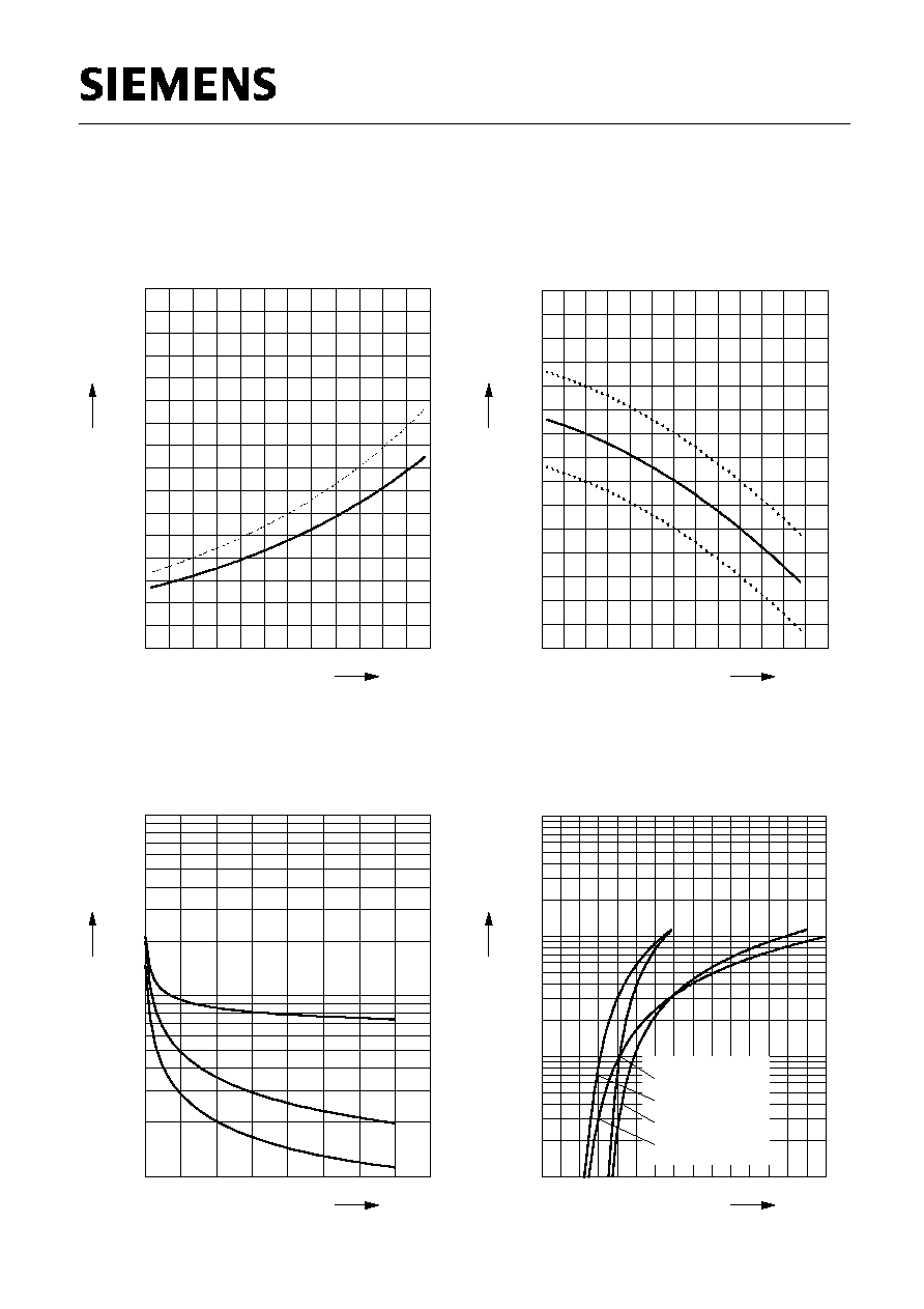
Typ. output characteristics
I
D
=
(
V
DS
)
parameter:
t
p
= 80 µs ,
T
j
= 25 ∞C
0.0
0.5
1.0
1.5
2.0
2.5
3.0
3.5
4.0
V
5.0
V
DS
0
5
10
15
20
25
30
35
40
45
50
55
A
65
I
D
V
GS
[V]
a
a
2.5
b
b
3.0
c
c
3.5
d
d
4.0
e
e
4.5
f
f
5.0
g
g
5.5
h
h
6.0
i
i
6.5
j
j
7.0
k
k
8.0
l
P
tot
= 75W
l
10.0
Typ. drain-source on-resistance
R
DS (on)
=
(
I
D
)
parameter:
t
p
= 80 µs,
T
j
= 25 ∞C
0
10
20
30
40
A
55
I
D
0.00
0.02
0.04
0.06
0.08
0.10
0.12
0.16
R
DS (on)
V
GS
[V] =
a
2.5
V
GS
[V] =
a
a
3.0
b
b
3.5
c
c
4.0
d
d
4.5
e
e
5.0
f
f
5.5
g
g
6.0
h
h
6.5
i
i
7.0
j
j
8.0
k
k
10.0
Typ. transfer characteristics
I
D
=
f (V
GS
)
parameter: t
p
= 80 µs
V
DS
2 x
I
D
x R
DS(on)max
0
1
2
3
4
5
6
7
8
V
10
V
GS
0
5
10
15
20
25
30
35
40
45
50
A
60
I
D
Semiconductor Group
7
30/Jan/1998
SPD28N05L
SPU28N05L
Drain-source on-resistance
R
DS (on)
=
(
T
j
)
parameter:
I
D
= 20 A,
V
GS
= 4.5 V
-60
-20
20
60
100
∞C
180
T
j
0.00
0.02
0.04
0.06
0.08
0.10
0.12
0.16
R
DS (on)
typ
98%
Gate threshold voltage
V
GS(th)
= f (T
j
)
parameter:
V
GS
=
V
DS
,
I
D
= 50µA
-60
-20
20
60
100
140
V
200
T
j
0.0
0.2
0.4
0.6
0.8
1.0
1.2
1.4
1.6
1.8
2.0
2.2
2.4
2.6
V
3.0
V
GS(th)
min
typ
max
Typ. capacitances
C = f (V
DS
)
parameter:V
GS
= 0V, f = 1MHz
0
5
10
15
20
25
30
V
40
V
DS
2
10
3
10
4
10
pF
C
C
iss
C
oss
C
rss
Forward characteristics of reverse diode
I
F
=
(
V
SD
)
parameter:
T
j
, t
p
= 80 µs
0
10
1
10
2
10
3
10
A
I
F
0.0
0.4
0.8
1.2
1.6
2.0
2.4
V
3.0
V
SD
T
j
= 25 ∞C typ
T
j
= 25 ∞C (98%)
T
j
= 175 ∞C typ
T
j
= 175 ∞C (98%)
Semiconductor Group
8
30/Jan/1998
SPD28N05L
SPU28N05L
Typ. gate charge
V
GS
=
(
Q
Gate
)
parameter:
I
D puls
= 28 A
0
5
10
15
20
25
30
35
40
nC
50
Q
Gate
0
2
4
6
8
10
12
V
16
V
GS
DS max
V
0,8
DS max
V
0,2
Drain-source breakdown voltage
V
(BR)DSS
=
(
T
j
)
-60
-20
20
60
100
∞C
180
T
j
49
51
53
55
57
59
61
V
65
V
(BR)DSS