Video Modulator for
FM/AM-Audio with
PLL-Output
Preliminary Data
Bipolar IC
TDA 5670-5X
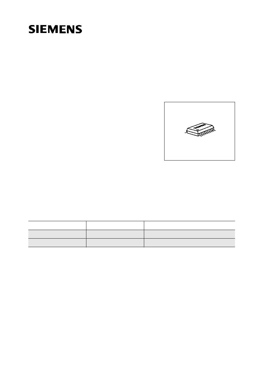
P-DSO-20 -1
Features
q
FM- and AM-audio modulator
q
Symmetrical RF-oscillator output for PLL-control
q
Sync level clamping of video input signal
q
Controlling of peak white value
q
Continuous adjustment of modulation depth for
positive or negative values
q
Symmetrical mixer output with separate ground area
q
Symmetrical oscillator with separate RF-ground
q
Low spurious radiation
q
High stability of the RF-oscillator frequency
q
High stability of the audio oscillator
q
Internal reference voltage
q
12 V supply voltage
Semiconductor Group
1
04.95
Functional Description and Application
The monolitic integrated circuit TDA 5670-5X is especially suitable as a modulator for the
48- to 860-MHz frequency range.
Video recorders, cable converters, TV-converter networks, demodulators, video
generators, video security systems, amateur TV-applications and personal computers.
Type
Ordering Code
Package
TDA 5670-5X
Q67000-A5167
P-DSO-20-1 (SMD)
TDA 5670-5X
Q67006-A5167
P-DSO-20-1 Tape & Reel

Semiconductor Group
2
TDA 5670-5X
Circuit Description
Oscillator
The RF-oscillator is available at pins 3-7. The oscillator operates as a symmetrical
Colpitts circuit. The oscillator chip ground, pin 5, should be connected to ground at the
resonance circuit shielding point. An external oscillator can be injected inductively or
capacitively via pins 3 and 7. The layout of the PCB should be such as to provide a
minimum shielding attenuation between the oscillator pins 3-7 and modulator output pins
15-17 of approximately 80 dB.
For optimal residual carrier suppression, the symmetrical mixer outputs at pins 15, 17
should be connected to a matched balanced-to-unbalanced broadband transformer, e.g.
a Guanella transformer with good phase precision at 0
o
and 180
o
. The transmission loss
should be less than 3 dB. In addition, an LC-low pass filter combination is required at the
output. The cut-off frequency of the low pass filter combination must exceed the
maximum operating frequency.
Video
The video signal with the negative synchronous level is capacitively connected to pin 12.
The internal clamping circuit is referenced to the synchronizing level. Should the video
signal change by 6 dB, this change will be compensated by the resonance circuit which
is set by the peak white value. At pin 13, the current pulses of the peak white detector are
filtered through the capacitor which also determines the control time constant. The RF-
carrier switches from negative to positive video modulation, when pin 14 is connected
to ground. By varying the value of resistance
R
at pin 14 between
... 0
the modulation
depth can be increased from 70% to 100% when the modulation is negative and
decreased from 100% to 70% when the modulation is positive.
Audio
Via pin 1, the audio signal is capacitively coupled to the AF-input for the FM-modulation
of the oscillator. A parallel resonance circuit is connected to the audio carrier oscillator at
pins 19, 20. The unloaded
Q
of the resonant circuit must be
Q
= 25 and the parallel
resistor
R
T
= 8.2 k
to ensure a video to audio carrier ratio of 12.5 dB. At the same time,
the capacitative and/or inductive reactance for the resonance frequency should have a
value of
X
C
X
L
800
.
Via pin 18, the audio signal is capacitively coupled to the AF-input for the AM-modulation
of the oscillator. This signal is forwarded to a mixer which is influenced by the AM-
modulation input of pin 18. The video to audio carrier ratio can be changed by connecting
an external voltage to pin 18, which deviates from the internal reference voltage.
Through an additional external dc voltage at pin 18, the set AM-modulation index can be
changed by overriding the internally adjusted control voltage for a fixed AM-modulation
index.
At the output of the above described mixer the FM and/or AM modulated audio signal is
added to the video signal and mixed with the oscillator signal in the RF-mixer.
Source
The internal reference voltage is available at pin 2 and has to be capacitively blocked
there.
TDA 5670-5X
Semiconductor Group
3
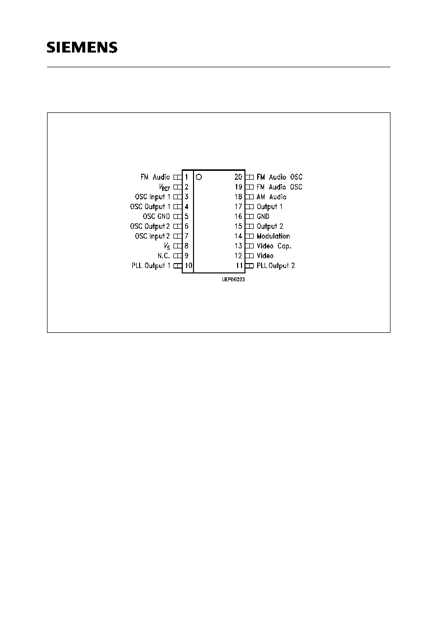
Pin Configuration
(top view)
P-DSO-20-1
Semiconductor Group
4
TDA 5670-5X
Pin Definitions and Functions
Pin No.
Symbol
Function
1
FM-Audio
AF-input for FM-modulation
2
V
REF
Internal reference voltage (7.5 V)
3
OSC-Input 1
Symmetrical oscillator input
4
OSC-Out 1
Symmetrical oscillator output
5
OSC-Ground
Oscillator ground
6
OSC-Out 2
Symmetrical oscillator output
7
OSC-Input 2
Symmetrical oscillator input
8
V
S
Supply voltage (12 V)
9
N.C.
Not connected
10
PLL-Out 1
Symmetrical unmodulated oscillator output
11
PLL-Out 2
Symmetrical unmodulated oscillator output
12
Video
Video input with clamping
13
Video-Cap.
Connection for smoothing capacitor for video control
loop
14
Modulation
Switch-over for positive and negative modulation
15
Output 2
Symmetrical RF-output
16
Ground
Ground
17
Output 1
Symmetrical RF-output
18
AM-Audio
Video to audio carrier ratio adjustment and AF-input for
AM-modulation
19
FM-Audio OSC
FM-audio oscillator; symmetrical inputs for tank circuit
20
FM-Audio OSC
FM-audio oscillator; symmetrical inputs for tank circuit
TDA 5670-5X
Semiconductor Group
5
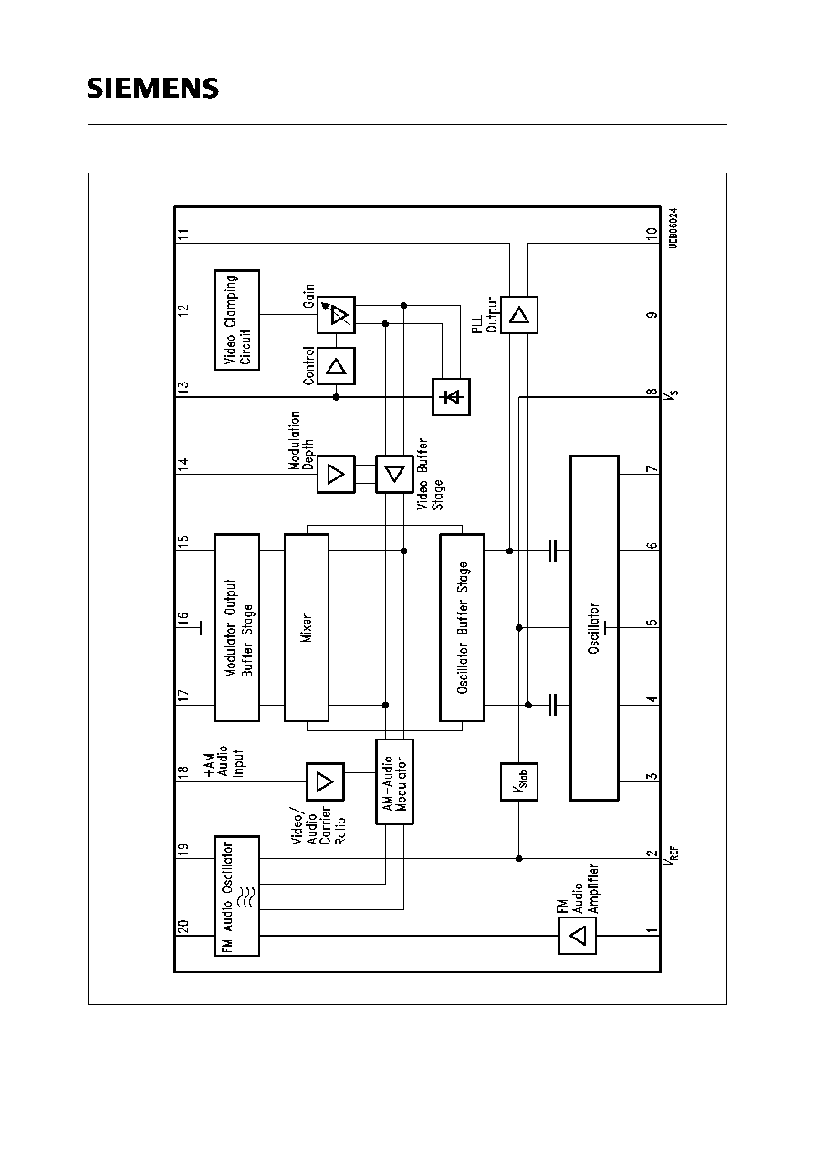
Block Diagram
Semiconductor Group
6
TDA 5670-5X
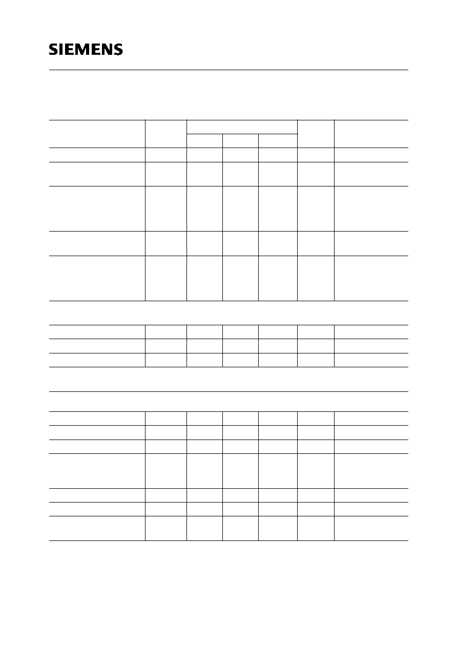
Absolute Maximum Ratings
T
A
= 0 to 70
o
C
Parameter
Symbol
Limit Values
Unit
Remarks
min.
typ.
max.
Supply voltage pin 8
V
S
� 0.3
14.5
V
Current from pin 2
�I
2
0
2
mA
V
2
= 7...8 V
V
S
= 10...13.5 V
Voltage at pin 1
Voltage at pin 2
Voltage at pin 12
V
1
V
2
V
10
0
6
0
2
8.5
1.5
V
V
Vpp
only via
C
(max. 1
�
F)
Capacitance at pin 2
Capacitance at pin 13
C
2
C
13
0
0
100
15
nF
�
F
Voltage at pin 14
Voltage at pin 15
Voltage at pin 17
Voltage at pin 18
V
14
V
15
V
17
V
18
� 0.3
V
2
V
2
V
2
-1.5
1.4
V
S
V
S
V
2
+1.5
V
V
V
V
V
S
= 10-13.5 V
According to the application circuit, only the provided circuitry can be connected
to pins 3,4,6,7,10,11,19 and 20.
Junction temperature
T
j
150
o
C
Storage temperature
T
stg
� 40
125
o
C
Thermal resistance
R
th
125
K/W
The pins 3, 4, 6 and 7 are not protected against voltage stress. The high frequency performance
prohibits the use of adequate protective structures.
Operating Range
Supply voltage
V
S
10
13.5
V
Video input frequency
f
Video
0
6
MHz
Audio input frequency
f
AF
0
20
kHz
Output frequency
f
Q
30
860
MHz
depending on the
oscillator circuitry
at pins 3-7
Ambient temperature
T
A
0
70
o
C
Audio oscillator
f
OSC
4
7
MHz
Voltage at pin 2
Voltage at pin 15,17
V
2
V
15, 17
6.75
V
2
7.75
V
S
V
V
TDA 5670-5X
Semiconductor Group
7
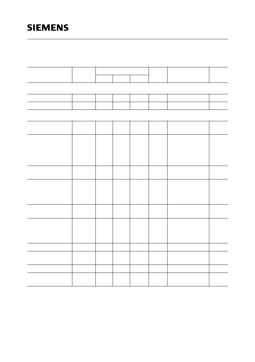
AC/DC-Characteristics
T
A
= 25
o
C;
V
S
= 12 V
Parameter
Symbol
Limit Values
Unit
Test
Condition
Test
Circuit
min.
typ.
max.
Source
Current consumption
I
8
22
28
34
mA
I
2
= 0 mA
1
Reference voltage
V
2
6.75
7.25
7.75
V
0
I
2
1 mA
1
Oscillator
Oscillator frequency
range
f
OSC
470
900
MHz
V
D
= 0...28 V
Oscillator drift
f
OSC
f
OSC
f
OSC
200
800
400
kHz
kHz
kHz
t
= 5 s-15 min.
after switching on
T
= 25
o
C
V
S
= 12 V
�
10%
T
A
= const.; Ch 40
1
1
1
Oscillator level
10;11
�20
�20
dBm
dBm
Ch 21
Ch 69
Oscillator output
impedance
R
10;
R
11
C
10;
C
11
200
2
pF
parallel
equivalent circuit
parallel
equivalent circuit
1
1
RF-output imp.
RF-output imp.
Z
15;
Z
17
C
15
=
C
17
0.5
150
1
2.0
pF
static
1
1
RF-output voltage
V
Q
2.5
4.5
5.5
mVrms Ch 40; video
100% white;
without audio-
signal
1
RF-output phase
15, 17
140
180
220
deg
RF-output voltage
changes
V
Q
0
1.5
dB
f
= 470-900 MHz
Intermodulation ratio
IMR
50
75
dB
f
VC
+ 1.07 MHz
2
Harmonic wave ratio
O
35
dB
f
VC
+ 8.8 MHz
without video
2
Semiconductor Group
8
TDA 5670-5X
Unmodulated video and audio carrier, measured with the spectrum analyzer as difference
between video carrier signal level and sideband signal level; loaded
Q
factor
Q
L
of the audio
oscillator resonance circuit adjusted by
R
P
to provide the required video to audio carrier ratio of
12.5 dB;
Q
U
= 25
Video to audio
carrier ratio
V/A
10
12.5
15
dB
f
VC
+
f
AC
(5.5 MHz)
1
Harmonic wave ratio
Harmonic wave ratio
O
O
35
42
48
48
dB
dB
f
VC
+ 2
f
AC
(11 MHz)
f
VC
+ 3
f
AC
(16.5 MHz)
1
1
All remaining harmonic waves; multiple of fundamental wave of video carrier, without video
signal, measured with spectrum analyzer;
f
VC
= 523.25-623.25 MHz; pin 14 open
15
dB
1
Residual carrier
suppression
R
32
dB
Ch 30...40
3
Signal-to-noise in
video; unmodulated
audio carrier
N/V
48
74
dB
Ch 30...40
4
Interference product
ratio audio in video
AM-modulation
FM-modulation of
audio carrier
A/V
A/V
49
48
62
60
dB
dB
Ch 30...40,
Ch 30...40
m
A
= 90%
4
4
Unweighted AM-
Unweighted FM-
interference level
ratio video in audio
V/A
V/A
48
48
54
54
dB
dB
Ch 39; test
picture FuBK
Ch 39; test
picture FuBK
5
5
Signal-to-noise ratio
of audio oscillator
N/A
N/A
48
48
54
54
dB
dB
AM unmodulated
FM-audio carrier
5
5
Video
Video input current
at pin 12
�I
12
0
1
�
A
C
12
100 nF
1
Video input voltage
at pin 12
V
12
0.7
1.4
Vpp
C
12
100 nF
1
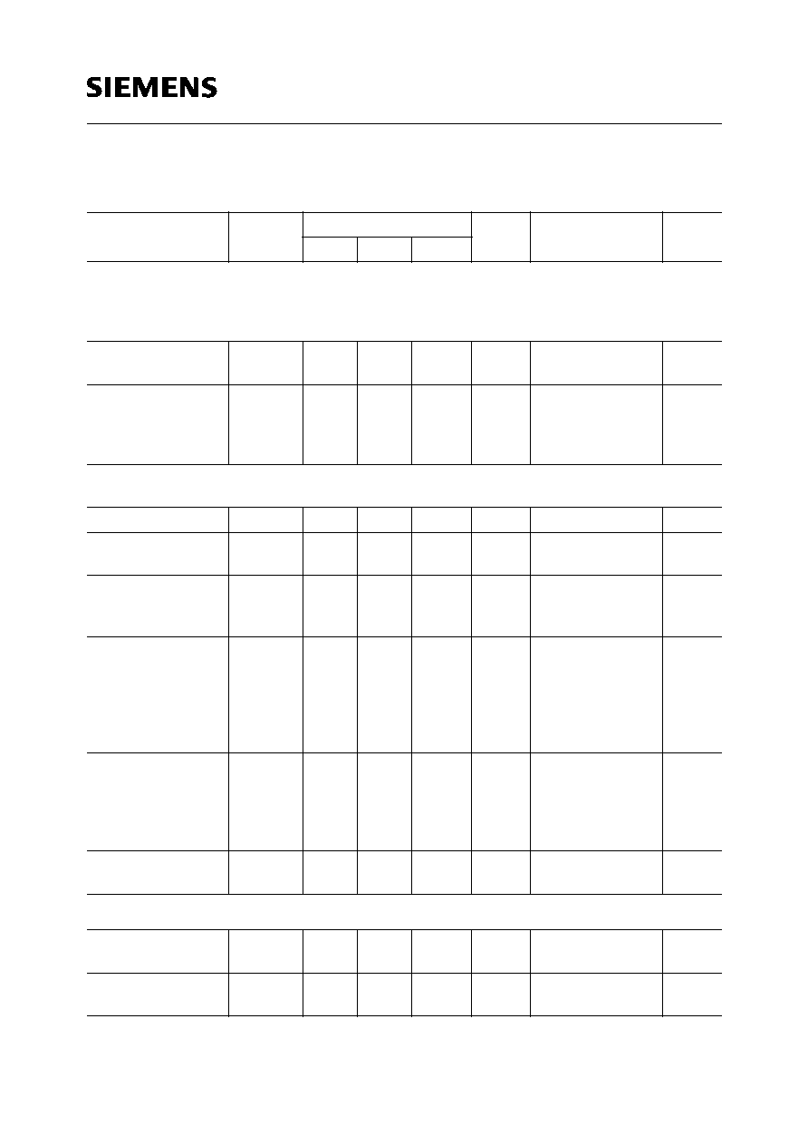
AC/DC-Characteristics (cont'd)
T
A
= 25
o
C;
V
S
= 12 V
Parameter
Symbol
Limit Values
Unit
Test
Condition
Test
Circuit
min.
typ.
max.
TDA 5670-5X
Semiconductor Group
9
Modulation depth
m
D/N
60
70
80
%
staircase signal at
video input;
V
Video
= 1 Vpp
6
Stability of mod.
depth
m
D
m
D
m
D
1
1
1
�
2.5
�
2.5
�
2.5
%
%
%
V
Video
= 1 Vpp
�
3 dB;
T
A
= 0-60
o
C
V
S
= 10-13.5 V
6
6
6
Differential gain
dif
10
%
7
Differential phase
dif
15
deg
measured with
measurement
demodulator,
video test signals
and vector scope
7
Amplitude response of video signal;
V
Video
= 1 Vpp with additional modulation
f
= 15 kHz-5MHz
sine signal between black and white
V
0
1.5
dB
8
Period of time required for peak white detector to reach steady state for full modulation depth with
1-white pulse per half frame when control is already in the steady state
t
6
50
�
s
C
at pin 13 =
10
�
F;
I
leakage
2
�
A
1
Setting time for video signal change from 0 Vpp to 1.4 Vpp; video blanking signal content is
uniform white level
t
120
500
�
s
1
Setting time for video blanking signal from 100% white level to 42% grey level with subsequent
rise in grey level to 71% of video blanking signal (due to decontrol process)
t
0.4
2
10
min
1
Audio
Audio oscillator frequency range; unloaded
Q
factor of resonance circuit
Q
u
= 25;
f
resonance
= 5.5 MHz
f
A/OSC
4
7
MHz
1
AC/DC-Characteristics (cont'd)
T
A
= 25
o
C;
V
S
= 12 V
Parameter
Symbol
Limit Values
Unit
Test
Condition
Test
Circuit
min.
typ.
max.
Semiconductor Group
10
TDA 5670-5X
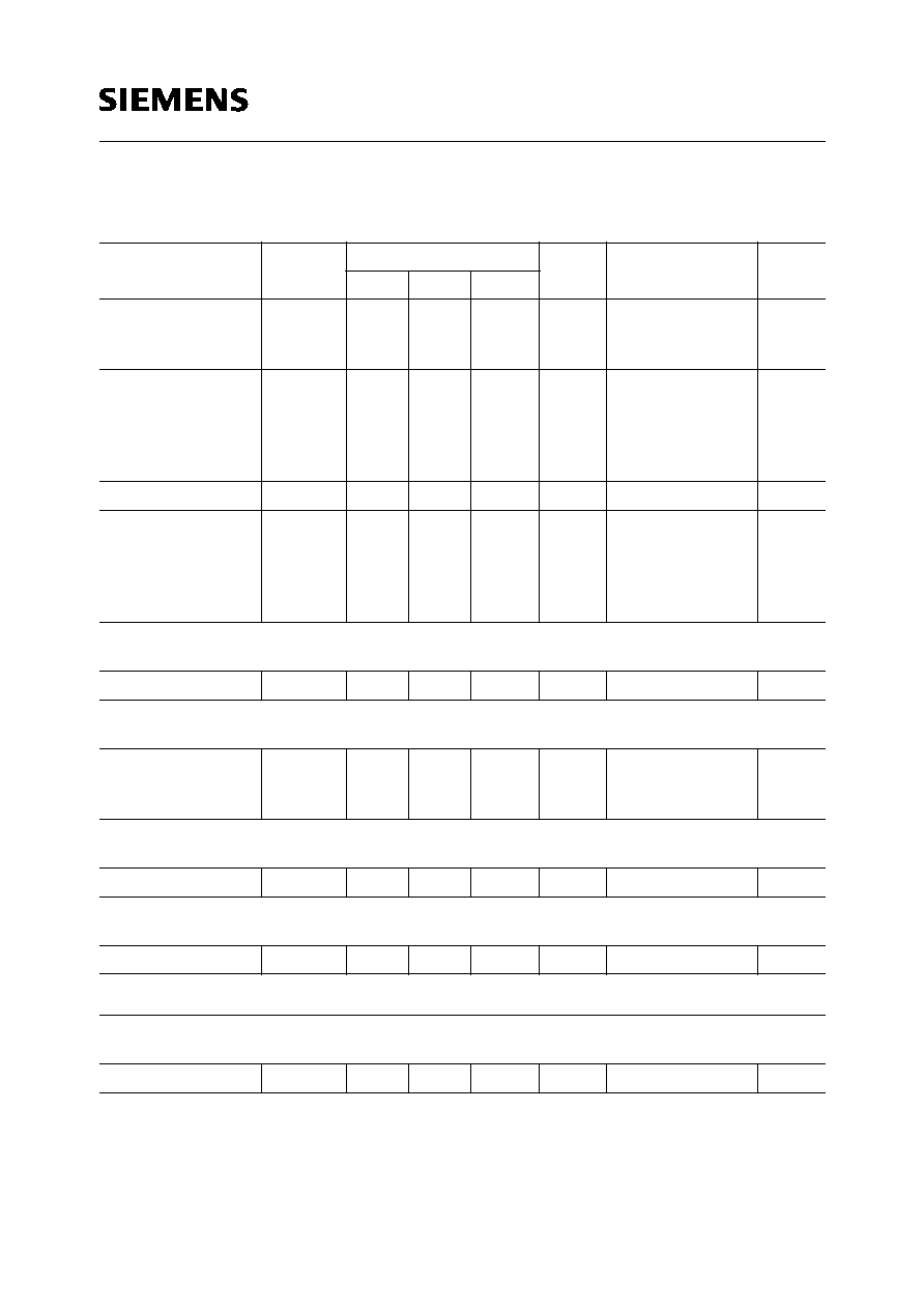
Switch-on, warm-up drift of oscillator frequency;
T
C
-value of capacitor in audio oscillator circuit
is 0, the drift is only based on self-heating of component
f
A/OSC
5
15
kHz
T
A
= const.;
1
Audio signal
frequency deviation
f
A/OSC
5
10
kHz
V
S
= 10.0-13.5 V;
Q
u
= 25
1
AM-Audio
AM-mod. factor
m
20
30
40
%
V
AF
= 45 mVrms
9
AM-mod.; total
harmonic distortion
THD
AM
0.5
3
%
m
= 80%;
V
AF
= 117 mVrms
f
AF
= 1 kHz
9
Audio preamplifier
input impedance
Z
16
25
50
75
k
1
AM-audio modulator
input voltage
V
AF
132
mVrms
m
= 90%;
f
AF
= 1 kHz
9
Residual carrier FM;
AM-operation
f
20
Hz
without AM-audio
signal
Q
U
= 25
1
FM-Audio
FM-mod.; total
harmonic distortion
THD
FM
0.6
1.5
%
V
1
= 150 mVrms
9
FM-mod.; static
mod. characteristic
f
A/OSC
�
50
�
70
�
90
kHz
V
AF
=
V
1
-
V
2
=
�
1 V
1
FM-mod.; dynamic
mod. characteristic
f
A/OSC
/
V
AF
0.08
0.10
0.13
kHz/
mV
1
Audio preamplifier
input impedance
(dynamic)
Z
1
200
k
1
AC/DC-Characteristics (cont'd)
T
A
= 25
o
C;
V
S
= 12 V
Parameter
Symbol
Limit Values
Unit
Test
Condition
Test
Circuit
min.
typ.
max.
TDA 5670-5X
Semiconductor Group
11
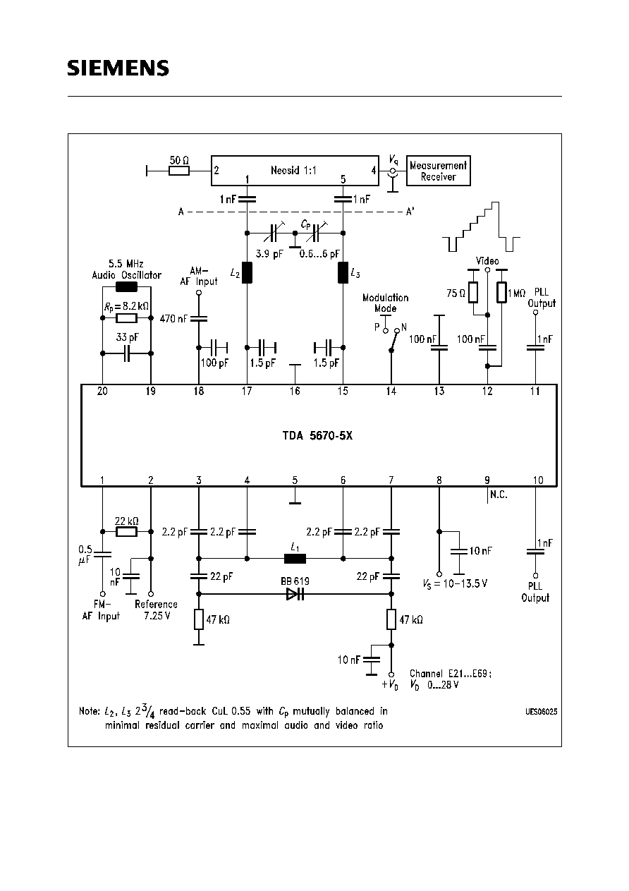
Test Circuit 1
Test and Measurement Circuit for AM- and FM-Audio Carrier and Negative Video
Modulation
Semiconductor Group
12
TDA 5670-5X
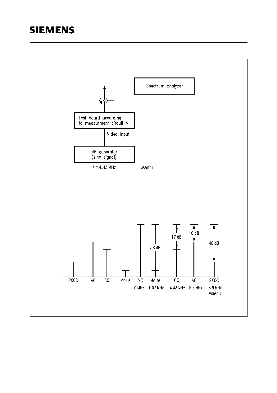
Test Circuit 2
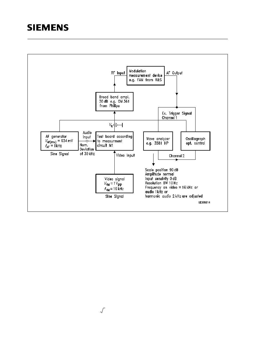
Description of the Measurement Configuration to Measure the 1.07-MHz Moire
CC-level lies below the activation point and has been set to provide a ratio of 17 dB with respect to
the video carrier.
f
VC
= 623.25 MHz
TDA 5670-5X
Semiconductor Group
13
Test Circuit 3
Description of the Measurement Configuration to Measure the Residual Carrier
Suppression
Semiconductor Group
14
TDA 5670-5X
Test Circuit 4
Description of the Measurement Configuration to Measure the Audio and/or Noise
in Video during FM- and AM-Modulation of the Audio Carrier
Calibration:
AF-signals are switched off, video signal is present at video input, modulation
measurement device set at AM is adjusted to video carrier; filter: 300 Hz...20 kHz;
detector: (P+P)/2; Wave analyzer at video signal level (16 kHz) adjusted and
resultant level as reference
a
v
defined.
1) Measurement of audio interference product ratio in video while the audio carrier FM modulated:
AF-signal is connected to FM-audio input; video signal is present at video input; Modulation
measurement device set at AM; filter: 300 Hz...20 kHz; detector: (P+P)/2; the automatic RF-level
position of the measurement device is switched off; wave analyzer at video signal level 1 kHz or
2 kHz or 3 kHz adjusted and resultant level is set to
a
A
.
The audio noise ratio in video results
from
a
A/V
=
a
A
-
a
V
(dB).
2) Measurement of signal-to-noise ratio in video without FM-modulation of audio carrier: AF-signals
are switched off; video signal is switched on; modulation measurement device set at AM; filter:
300 Hz...3 kHz; detector: RMS x
; Wave analyzer at video signal level (16 kHz) detuned; read
out in dB to reference level of calibration is
a
N/V
.
3) The noise limit of the measurement device is approx. 85 dB.
2
TDA 5670-5X
Semiconductor Group
15
Test Circuit 5
Description of the Measurement Configuration to Measure the Video and/or Noise
in Audio
Calibration:
AF-signal of
f
= 1 kHz, corresponding with a nominal deviation of 30 kHz, is
connected to the audio input, and the demodulated AF-reference level at the audio
measurement device is defined as 0 dB. No video signal is present.
Measuring:
1) The AF-signal is switched off and the FuBK-video signal is connected to the video
input with
V
vid
= 1 Vpp. The audio level in relation to the AF-reference calibration
level is measured as ratio
a
V/A
.
2) AF- and video signal are switched off. The noise ratio in relation to the AF-
reference calibration level is measured as signal-to-noise ratio in the audio signal
a
N/A
.
Semiconductor Group
16
TDA 5670-5X
Test Circuit 6
Description of the Measurement Configuration to Measure the Modulation Depth
for Positive and Negative Modulation
Calibration:
A zero reference signal with the TV-measuring receiver is given to the video signal.
A video signal with
V
vid
= 1 Vpp is connected to the video input.
Measuring:
1) Modulation depth
m
D/N
for negative modulation: pin 14 open, range peak white
value
�
sync level in relation to range zero reference
�
sync level gives
m
D/N
.
2) Modulation depth
m
D/P
for positive modulation: pin 14 to ground, range peak
white value � sync level in relation to range zero reference � peak white value gives
m
D/P
.
TDA 5670-5X
Semiconductor Group
17
Test Circuit 7
Description of the Measurement Configuration to Measure the Differential Gain
and Phase
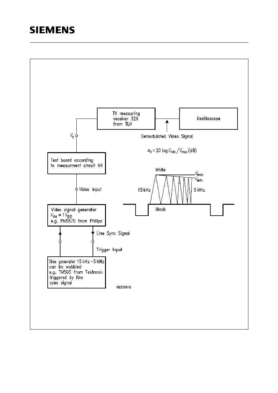
Semiconductor Group
18
TDA 5670-5X
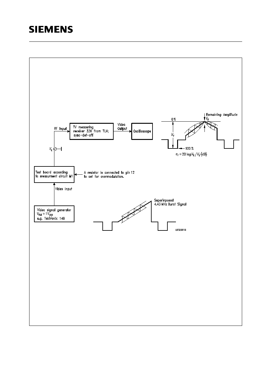
Test Circuit 8
Description of the Measurement Configuration to Measure the Video Amplitude
Response
TDA 5670-5X
Semiconductor Group
19
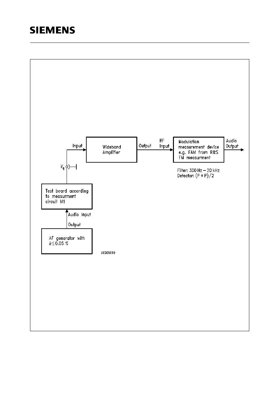
Test Circuit 9
Description of the Measurement Configuration to Measure the Harmonic
Distorsion Factor and AM-Input Voltag
Semiconductor Group
20
TDA 5670-5X
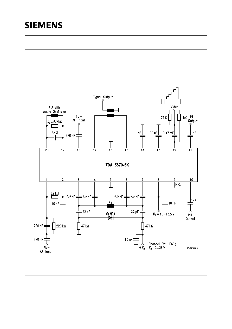
Application Circuit
TDA 5670-5X
Semiconductor Group
21
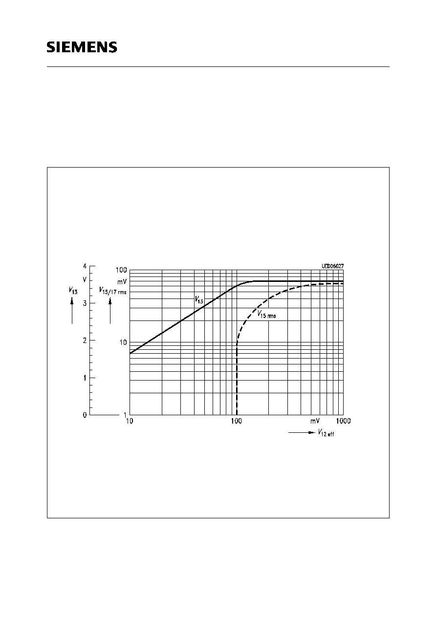
Diagram
Function of Video Signal Connection
a) Demodulated RF-output video signal
V
15/17rms
=
f
(
V
12rms
);
f
mod
= 16 kHz
b)
V
13
=
f
(
V
12rms
)
Semiconductor Group
22
TDA 5670-5X
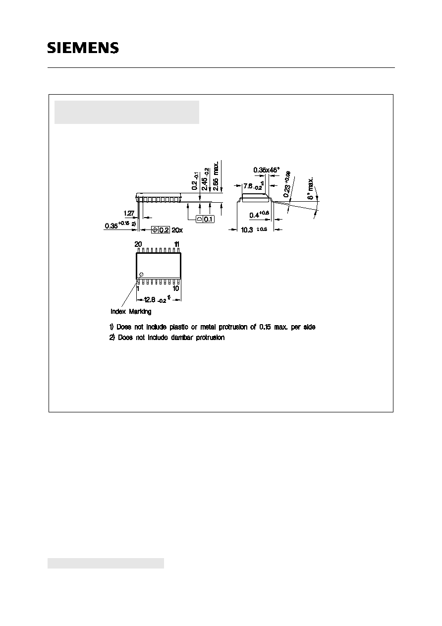
Plastic Package, P-DSO-20-1 (SMD)
(Plastic Dual Small Outline Package)
GPS05094
Sorts of Packing
Package outlines for tubes, trays etc. are contained in our
Data Book "Package Information"
Dimensions in mm
SMD = Surface Mounted Device