 | –≠–ª–µ–∫—Ç—Ä–æ–Ω–Ω—ã–π –∫–æ–º–ø–æ–Ω–µ–Ω—Ç: TLE4260S | –°–∫–∞—á–∞—Ç—å:  PDF PDF  ZIP ZIP |
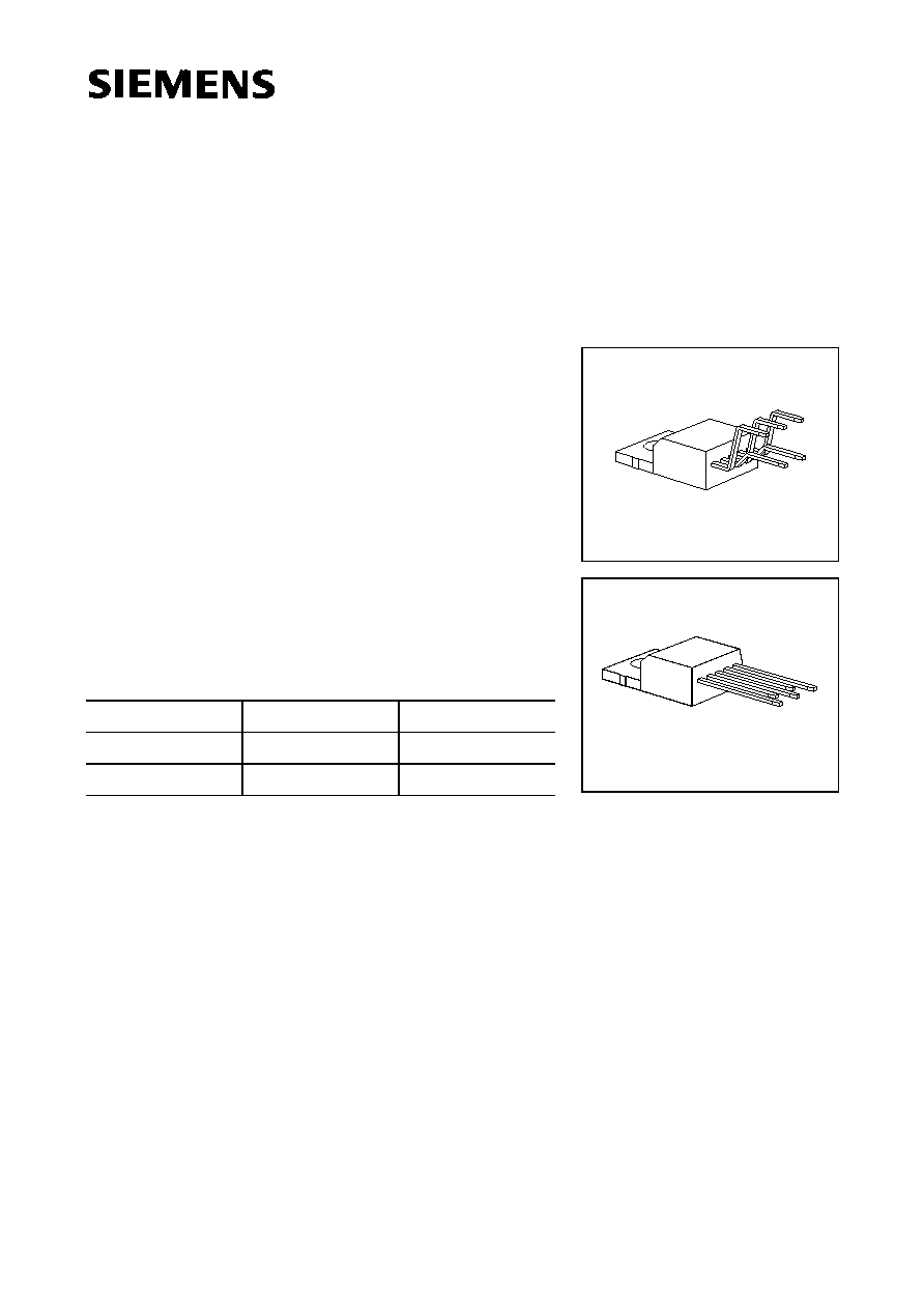
P-TO220-5-1
P-TO220-5-2
5-V Low-Drop Voltage Regulator
TLE 4260
Semiconductor Group
1
1998-11-01
Features
∑ Low-drop voltage
∑ Very low quiescent current
∑ Low starting current consumption
∑ Integrated temperature protection
∑ Protection against reverse polarity
∑ Input voltage up to 42 V
∑ Overvoltage protection up to 65 V (
400 ms)
∑ Short-circuit proof
∑ Suited for automotive electronics
∑ Wide temperature range
∑ EMC proofed (100 V/m)
Type
Ordering Code
Package
w
TLE 4260
Q67000-A8187
P-TO220-5-1
w
TLE 4260 S
Q67000-A9044
P-TO220-5-2
w
Please also refer to the new pin compatible device TLE 4270
Functional Description
TLE 4260; S is a 5-V low-drop fixed-voltage regulator in a P-TO220-5-H/S package. The
maximum input voltage is 42 V (65 V/
400 ms). The device can produce an output
current of more than 500 mA. It is shortcircuit-proof and incorporates temperature
protection that disables the circuit at unpermissibly high temperatures.
Due to the wide temperature range of ≠ 40 to 150
∞
C, the TLE 4260; S is also suitable
for use in automotive applications.
The IC regulates an input voltage
V
I
in the range 6 <
V
I
< 35 V to
V
Qnominal
= 5.0 V. A reset
signal is generated for an output voltage of
V
Q
< 4.75 V.
The reset delay can be set
externally with a capacitor. If the output current is reduced below 10 mA, the regulator
switches internally to standby and the reset generator is turned off. The standby current
drops to max. 700
µ
A.
TLE 4260
Semiconductor Group
2
1998-11-01
Pin Configuration
(top view)
Pin Definitions and Functions (TLE 4260 and TLE 4260 S)
Pin No.
Symbol
Function
1
V
I
Input; block directly to ground at the IC by a 470-nF capacitor
2
QVRES
Reset output; open collector output controlled by the reset
delay
3
GND
Ground
4
DRES
Reset delay; wired to ground with a capacitor
5
V
Q
5-V output voltage; block to ground with a 22-
µ
F capacitor
AEP00577
1
2
3
4
5
V
QVRES
GND
DRES
V
Q
TLE 4260
TLE 4260 S
TLE 4260
Semiconductor Group
3
1998-11-01
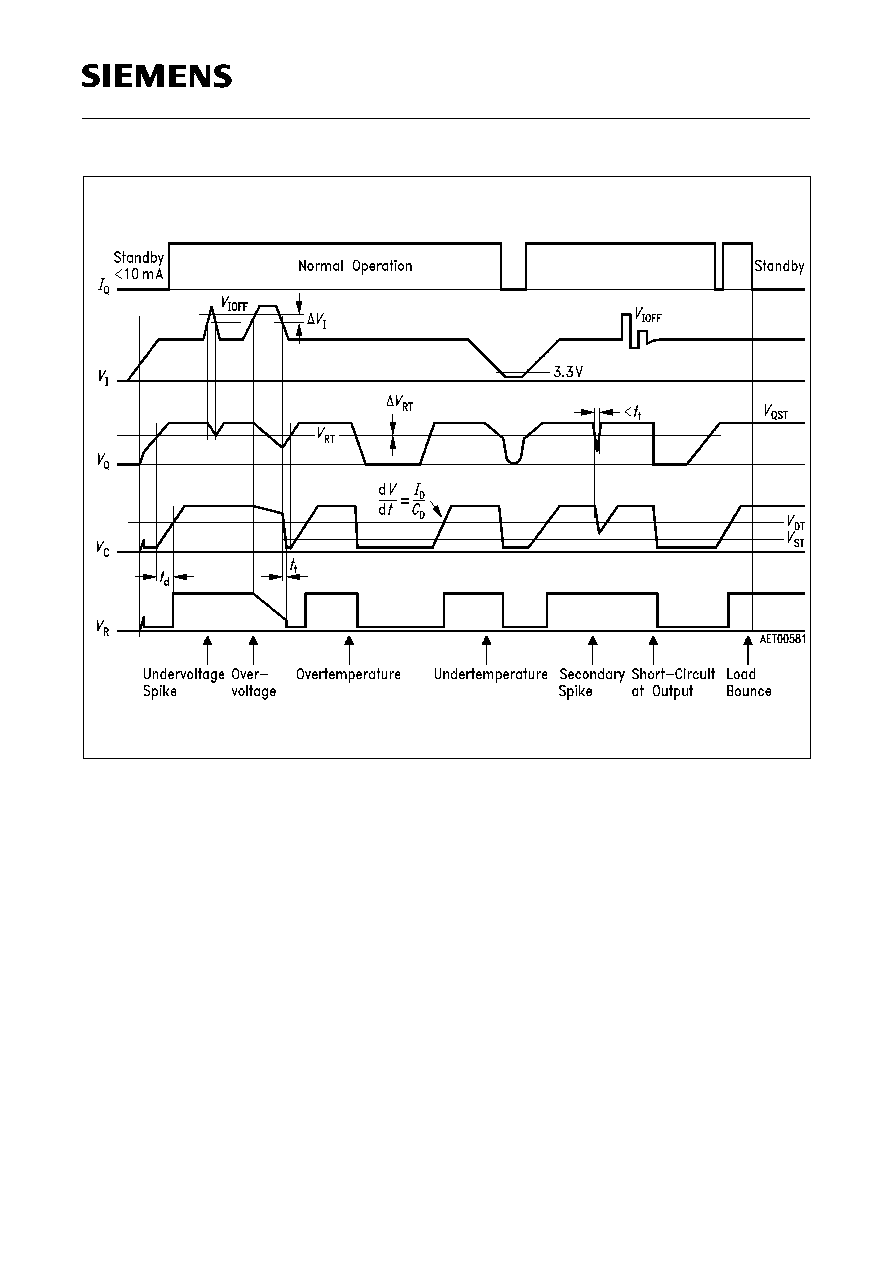
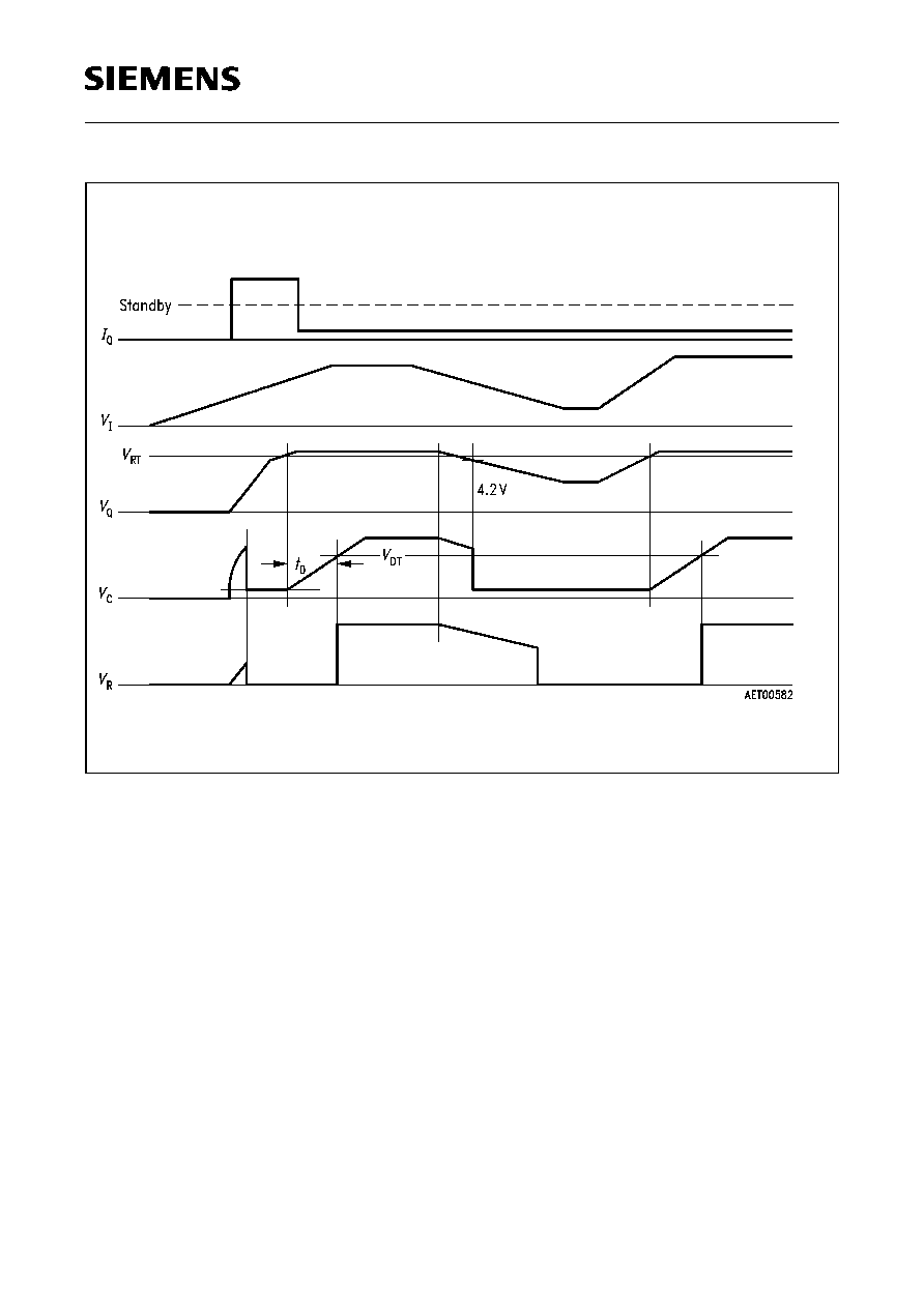
Circuit Description
The control amplifier compares a reference voltage, which is kept highly accurate by
resistance adjustment, to a voltage that is proportional to the output voltage and drives
the base of the series transistor via a buffer. Saturation control as a function of the load
current prevents any over-saturation of the power element. If the output voltage goes
below 96% of its typical value, an external capacitor is discharged on pin 4 by the reset
generator. If the voltage on the capacitor reaches the lower threshold
V
ST
, a reset signal
is issued on pin 2 and not cancelled again until the upper threshold
V
DT
is exceeded. For
an output current of less than
I
QN Off
= 10 mA the standby changeover turns off the reset
generator. The latter is turned on again when the output current increases, the output
voltage drops below 4.2 V or the delay capacitor is discharged by external measures.
The IC also incorporates a number of internal circuits for protection against:
∑ Overload
∑ Overvoltage
∑ Overtemperature
∑ Reverse polarity
Block Diagram
Overvoltage
Monitoring
Saturation
Control and
Protection
RESET
Generator
Temperature
Sensor
Adjustment
BANDGAP
Reference
-
+
7
4
2
3
1
Input
GND
Output
RESET
Delay
RESET
AEB00578
Circuit
STANDBY
Changeover
Amplifier
Control
Buffer
TLE 4260
Semiconductor Group
4
1998-11-01
Absolute Maximum Ratings
Parameter
Symbol
Limit Values
Unit
Remarks
min.
max.
Input (Pin 1)
Input voltage
V
I
≠ 42
42
V
≠
V
I
≠
65
V
t
400 ms
Input current
I
I
≠
1.6
A
≠
Reset Output (Pin 2)
Voltage
V
R
≠ 0.3
42
V
≠
Current
I
R
≠
≠
≠
internally limited
Ground (Pin 3)
Current
I
GND
≠ 0.5
≠
A
≠
Reset Delay (Pin 4)
Voltage
V
D
≠ 0.3
42
V
≠
Current
I
D
≠
≠
≠
internally limited
Output (Pin 5)
Differential voltage
V
I
≠
V
Q
≠ 5.25
V
I
V
≠
Current
I
Q
≠
1.4
A
≠
Temperature
Junction temperature
T
j
≠
32
∞
C
≠
Storage temperature
T
stg
≠ 50
150
∞
C
≠
TLE 4260
Semiconductor Group
5
1998-11-01
Operating Range
Parameter
Symbol
Limit Values
Unit
Remarks
min.
max.
Input voltage
V
I
≠
32
V
1)
Junction temperature
T
j
≠ 40
165
∞
C
≠
Thermal Resistances
Junction ambient
R
thja
≠
65
K/W
≠
Junction case
R
thjc
≠ 3
K/W
≠
1)
See diagram "Output Current versus Input Voltage"
TLE 4260
Semiconductor Group
6
1998-11-01
Characteristics
V
I
= 13.5 V;
T
j
= 25
∞
C; (unless otherwise specified)
Parameter
Symbol
Limit Values
Unit Test Condition
min.
typ.
max.
Normal Operation
Output voltage
V
Q
4.75
5.0
5.25
V
25 mA
I
Q
500 mA
6 V
V
I
28 V
≠ 40
∞
C
T
j
125
∞
C
Short -circuit current
I
SC
500
1000 ≠
mA
V
I
=17 V to 28 V;
V
Q
= 0 V
Current consumption
I
q
=
I
I
≠
I
Q
I
q
≠
8.5
10
mA
1)
6 V
V
I
28 V
I
Q
= 150 mA
Current consumption
I
q
=
I
I
≠
I
Q
I
q
≠
50
65
mA
1)
6 V
V
I
28 V
I
Q
= 500 mA
Current consumption
I
q
=
I
I
≠
I
Q
I
q
≠
≠
80
mA
1)
V
I
6 V
I
Q
= 500 mA
Drop voltage
V
DR
≠
0.35
0.5
V
V
I
= 4.5 V;
I
Q
= 0.5 A
Drop voltage
V
DR
≠
0.2
0.3
V
V
I
= 4.5 V;
I
Q
= 0.15 A
Load regulation
V
Q
≠
15
35
mV
25 mA
I
Q
500 mA
Supply-voltage regulation
V
Q
≠
15
50
mV
V
I
6 V to 28 V;
I
Q
= 100 mA
Supply-voltage regulation
V
Q
≠
5
25
mV
V
I
6 V to 16 V;
I
Q
= 100 mA
Ripple rejection
SVR
≠
54
≠
dB
f
= 100 Hz;
V
r
= 0.5 V
pp
Temperature drift of
output voltage
1)
VQ
≠
2
◊
10
≠4
≠
1/
∞
C ≠
Standby Operation
Quiscent current;
I
q
=
I
I
≠
I
Q
I
q
≠
500
700
µ
A
10 V
V
I
16 V;
I
Q
= 0 mA
Quiscent current;
I
q
=
I
I
≠
I
Q
I
q
≠
750
850
µ
A
10 V
V
I
16 V;
I
Q
= 5 mA
TLE 4260
Semiconductor Group
7
1998-11-01
Standby Off/Normal On
Current consumption
I
qSOFF
≠
1.0
1.2
mA
see test diagram
Current consumption
I
qNON
≠
1.7
2.2
mA
see test diagram
Normal Off/Standby On
Current consumption
I
qNOFF
≠
1.55
2.00
mA
see test diagram
Current consumption
I
qSON
≠
850
1050
µ
A
see test diagram
Switching threshold
I
QNOFF
7.5
10
12.5
mA
see test diagram
Switching hysteresis
I
Q
2.25
3
4
mA
see test diagram
Reset Generator
Switching threshold
V
RT
94
96
97
%
in % of
V
Q
;
I
Q
> 500 mA;
V
I
= 6 V
Saturation voltage
V
R
≠
0.25
0.40
V
I
R
= 3 mA;
V
I
= 4.5 V
Reverse current
I
R
≠
≠
1
µ
A
V
R
= 5 V
Charge current
I
D
7
10
13
µ
A
≠
Switching threshold
V
ST
0.9
1.1
1.3
V
≠
Delay switching threshold
V
DT
2.15
2.50
2.75
V
≠
Delay time
t
D
≠
25
≠
ms
C
D
= 100 nF
Delay time
t
t
≠
5
≠
µ
s
C
D
= 100 nF
General Data
Turn-Off voltage
V
IOFF
40
43
45
V
I
Q
< 1 mA
Turn-Off hysteresis
V
I
≠
3.0
≠
V
≠
Leakage current
I
QS
≠
500
≠
µ
A
V
Q
=
0 V;
V
I
=
45 V
Reverse output current
I
QR
≠
≠
1.5
mA
V
Q
=
5 V;
V
I
=
open
1)
See diagram
Characteristics (cont'd)
V
I
= 13.5 V;
T
j
= 25
∞
C; (unless otherwise specified)
Parameter
Symbol
Limit Values
Unit Test Condition
min.
typ.
max.
TLE 4260
Semiconductor Group
8
1998-11-01
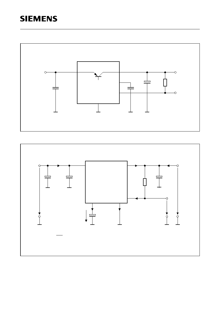
Application Circuit
Test Circuit
AES00579
TLE 4260
22 F
µ
1
5
Input
6V to 40V
Output
RESET
4
2
3
470 nF
100 nF
100 k
AES01509
TLE 4260-2
1000 F
µ
V
+
V
R
R
V
Q
V
d
GND
Q
SC
QS
C
d
100 nF
V
C
/
/
QR
R
22 F
µ
1.8 k
1
5
2
4
3
Q
V
+
V
V
Dr
=
SVR
V
R
V
Q
470 nF
= 20 log
TLE 4260
Semiconductor Group
9
1998-11-01
Time Responce
TLE 4260
Semiconductor Group
10
1998-11-01
Time Responce in Standby Condition
TLE 4260
Semiconductor Group
11
1998-11-01
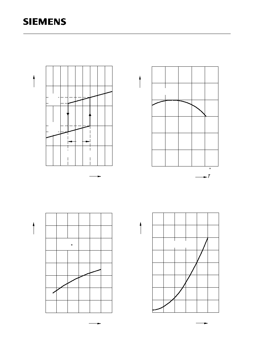
Standby/Normal Changeover
Drop Voltage versus Output Current
Output Voltage versus Temperature
Current Consumption versus
Output Current
AED00583
0
7
mA
mA
Q
8
9
10 11 12 13 14
16
0.5
1.0
1.5
2.0
2.5
N ON
OFF
N
ON
S
S
OFF
OFF
QN
QN
ON
Q
AED00584
0
0
100
200
300
600
mA
400
800
Q
400
100
300
500
600
700
200
D
Dr
V
= 4.5 V
= 25 C
mV
T
j
AED00028
4.60
-40
V
Q
0
40
80
160
4.70
4.80
4.90
5.00
5.10
5.20
V
V
=
120 C
j
13.5 V
AED00585
0
0
100
200
300
600
mA
40
80
mA
= 13.5 V
V
Q
400
10
30
50
60
70
20
TLE 4260
Semiconductor Group
12
1998-11-01
Current Consumption versus
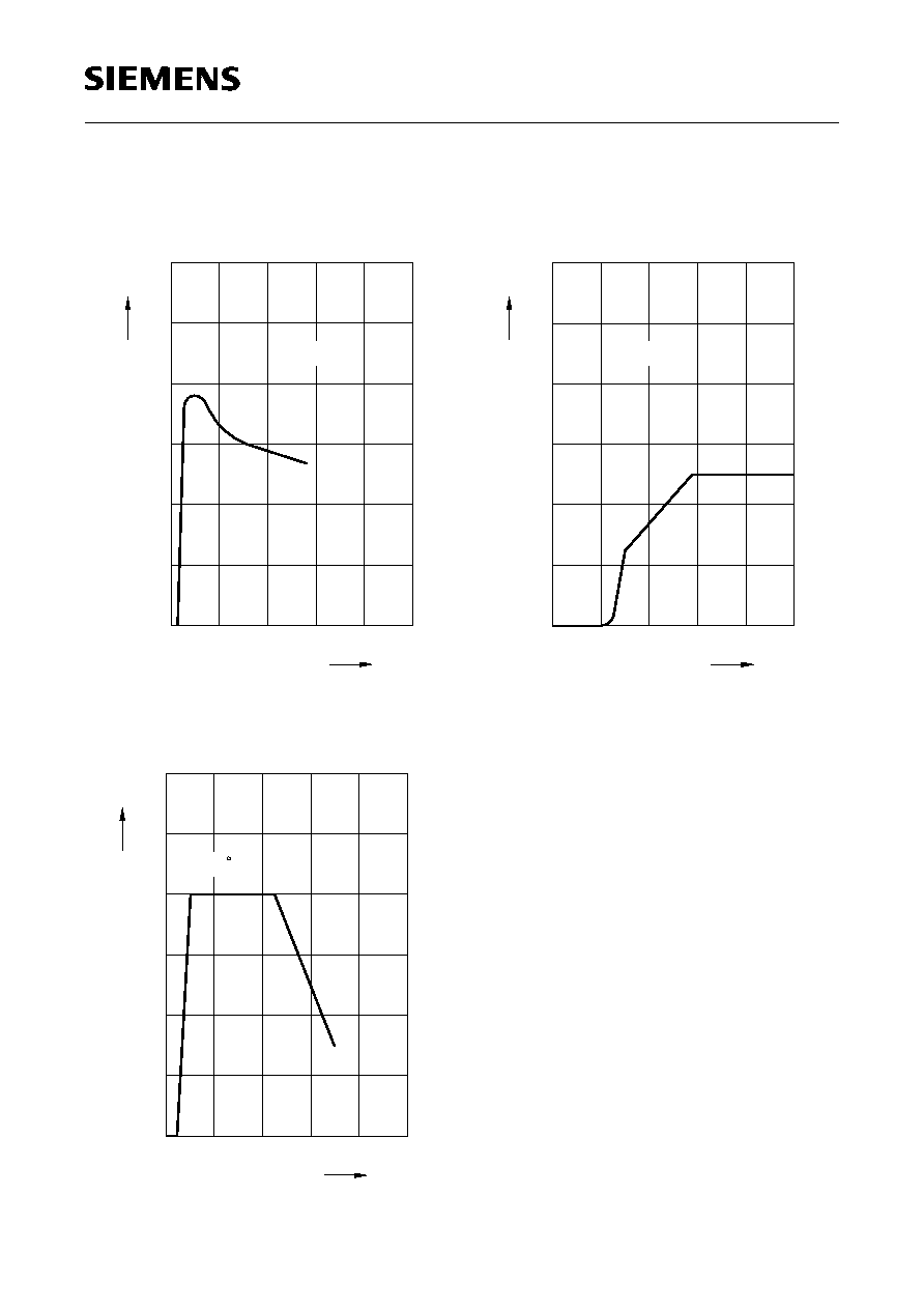
Input Voltage
Output Current versus Input Voltage
Output Voltage versus Input Voltage
AED00590
0
0
V
10
20
30
50
V
20
40
60
80
100
120
mA
R
L
= 10
40
AED00587
0
0
V
Q
10
20
30
50
V
A
40
1.2
1.0
0.8
0.6
0.4
0.2
C
= 25
T
j
AED00591
0
0
V
V
Q
2
4
6
10
V
2
4
6
8
10
12
V
R
L
= 10
8
TLE 4260
Semiconductor Group
13
1998-11-01
Package Outlines
10
+0.4
3.75
+0.1
1
5
1.7
0.8
8.4
±0.4
±0.4
4.5
0.4
+0.1
10.2
15.4
±0.3
8.8
-0.2
16
1.27
+0.1
-0.2
10.2
+0.1
2.8
4.6
-0.2
2.6
8.6
±0.3
±0.3
±0.4
19.5 max
1x45∞
1)
1) 1 at dam bar (max 1.8 from body)
1) 1 im Dichtstegbereich (max 1.8 vom Kˆrper)
-0.15
-0.15
M
0.6
5x
P-TO220-5-1
(Plastic Transistor Single Outline)
G
P
T
0
5
107
Weigth approx. 2.1 g
Sorts of Packing
Package outlines for tubes, trays etc. are contained in our
Data Book "Package Information".
Dimensions in mm
TLE 4260
Semiconductor Group
14
1998-11-01
10
+0.4
3.75
+0.1
1
5
1.7
0.8
±0.15
0.4
+0.1
15.4
±0.3
8.8
-0.2
1.27
+0.1
-0.2
10.2
+0.1
2.8
4.6
-0.2
2.6
10.9
±0.2
±0.2
12.9
1x45∞
1)
1) 1 at dam bar (max 1.8 from body)
1) 1 im Dichtstegbereich (max 1.8 vom Kˆrper)
-0.15
-0.15
M
0.6
5x
P-TO220-5-1
(Plastic Transistor Single Outline)
G
P
T
0
5
256
Weigth approx. 2.1 g
Sorts of Packing
Package outlines for tubes, trays etc. are contained in our
Data Book "Package Information".
Dimensions in mm