 | –≠–ª–µ–∫—Ç—Ä–æ–Ω–Ω—ã–π –∫–æ–º–ø–æ–Ω–µ–Ω—Ç: D602 | –°–∫–∞—á–∞—Ç—å:  PDF PDF  ZIP ZIP |

D602
3V, 6GHz Divide-by-2 Static Prescaler
Final
Applications
5GHz WLAN, IEEE 802.11a and HIPERLAN
VSAT at 3.6 to 4.2 GHz
Satellite Communications at 4.5 to 4.8 GHz
5 Gbps Clock Generator
Features
Low Phase Noise, -141dBc/Hz at 1kHz offset
Single Supply Voltage, 2.7 - 4.0 V
Low Power Consumption, 42mW
Power Down Mode, 0.2µA
Compatible with common PLL synthesizer ICs
8-Pin Plastic SOIC Package
Ordering Information
Type
Package
Remark
D602 8-Pin
SOIC Plastic
Package
Product Description
The D602 is a SiGe divide-by-2 low noise static
prescaler capable of operation up to 6.0 GHz. The
D602 operates over a wide range of input frequencies
and levels, and provides differential outputs for low
noise operation with the common PLL style frequency
synthesizer ICs.
The static nature of the prescaler prevents spurious
generation.
The D602 prescaler can operate from either a single
positive or single negative supply with power down
mode for low standby power consumption.
Functional Block Diagram
f
In
f
Out
In
Out
Out
In
V
CC
V
EE
V
EE
PWD
2
˜
20-DST-01 Rev 5.0 Sept/01
1 of 8

D602
3V, 6GHz Divide-by-2 Static Prescaler
Final
Pin Out Diagram
In
Out
Out
In
V
EE
V
EE
PWD
V
CC
D602
1
2
3
4
8
7
6
5
Pin Out Description
Pin No.
Name
Description
1 V
CC
Power Supply Voltage Input
2
In
Prescaler Input (internally-biased)
3
In
Prescaler Complementary Input (internally-biased)
4 V
EE
Ground for Input (pins 4 and 5 must be connected to the same potential)
5 V
EE
Ground for Output (pins 4 and 5 must be connected to the same potential)
6
Out
Complementary Output (open-collector)
7 Out
Output
(open-collector)
8 PWD
Power Down high impedance CMOS input. When PWD is high, the part is powered
down.
Absolute Maximum Ratings
Operation in excess of any one of above Absolute Maximum Ratings may result in permanent damage. This device is
a high performance RF integrated and is ESD sensitive. The RF inputs on this device are Class 0 ESD rated;
therefore suitable precaution should be taken during handling, assembly and testing.
Symbol
Parameter
Min.
Max.
Unit
Supply
Voltage -0.3
+4.3
V
Voltage on any pin with respect to V
EE
-0.3
V
CC
+ 0.3
V
Differential input voltage
-2.0
+2.0
V
Storage
Temperature
-65
+150
∞C
20-DST-01 Rev 5.0 Sept/01
2 of 8

D602
3V, 6GHz Divide-by-2 Static Prescaler
Final
Electrical Characteristics
Conditions: V
CC
= 3.0V, -40∞C < T
A
< 85∞C unless otherwise specified
Symbol
Parameter
Note
Min.
Typ.
Max.
Unit
V
CC
Supply
Voltage
2.7 3.0 4.0
V
T
A
Operating
Temperature 1
-40
25
85
∞C
I
CC
Supply
Current
14
18
mA
I
CC ≠ PWDN
Power-Down Supply Current
(V
PWD
= High)
0.2 1.0 µA
f
In(U)
Upper Limit of Input Frequency
2
5.8
6.4
GHz
f
In(L)
Lower Limit of Input Frequency
2
0.6
1.0
GHz
f
Osc
Self Oscillation Output Frequency
3
1.0
GHz
P
In(U)
Upper Limit of Input Power
0
3
dBm
P
In(L)
Lower Limit of Input Power
-20
-10
dBm
P
Out
Output
Power
4 -15.0
0
dBm
V
IH
High-Level PWD Input Voltage
V
CC
- 0.2
V
V
IL
Low-Level PWD Input Voltage
0.2
V
I
IH
High-Level PWD Input Current
-100.0
100.0
nA
I
IL
Low-Level PWD Input Current
-100.0
100.0
nA
PN
Residual Phase Noise at 1kHz offset from
a 2.5GHz (f
Out
) carrier
-141 dBc/Hz
Notes: (1) Sample
Tested
(2) For a sine-wave input
(3) Since the input signal is AC coupled, in the absence of an RF input, the prescaler may self oscillate and
provide an output at this frequency. Self oscillation can be eliminated by powering down the prescaler,
or applying a differential DC input voltage (a 47k resistor placed between pin 3 and V
CC
).
(4) This power is delivered to a 50 load. It excludes the power dissipated in the external pull-up resistors.
Test Circuit
D602
1
2
3
4
8
7
6
5
100p
100n
V
CC
1p
1n
51
51
1n
1n
Signal
Generator
50 Ohm
Measurement
Equipment
100p
100n
20-DST-01 Rev 5.0 Sept/01
3 of 8
D602
3V, 6GHz Divide-by-2 Static Prescaler
Final
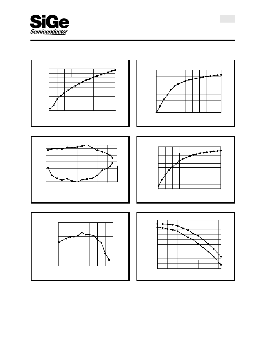
Typical Performance Characteristics
8
9
10
11
12
13
14
15
16
17
2.2
2.4
2.6
2.8
3.0
3.2
3.4
3.6
3.8
4.0
Supply Current vs Supply Voltage
Supply Voltage [V]
S
uppl
y
C
u
rrent
[mA
]
5.5
5.7
5.9
6.1
6.3
6.5
6.7
6.9
2.2
2.4
2.6
2.8
3.0
3.2
3.4
3.6
3.8
4.0
Upper Limit of Input Frequency vs Supply Voltage
PIn = ≠ 10dBm
Supply Voltage [V]
Input F
r
eque
ncy [GH
z
]
-40
-30
-20
-10
0
10
0.0
1.0
2.0
3.0
4.0
5.0
6.0
7.0
Input Power Limits vs Input Frequency
Input Frequency [GHz]
Input P
o
w
e
r [
d
B
m
]
P
In
(U)
P
In
(L)
-12
-11
-10
-9
-8
-7
-6
-5
-4
-3
-2
2.2
2.4
2.6
2.8
3.0
3.2
3.4
3.6
3.8
4.0
Output Power vs Supply Voltage
fIn = 5.0 GHz
Supply Voltage [V]
Output P
o
we
r [
d
B
m
,]
-15
-10
-5
0
0.0
1.0
2.0
3.0
4.0
5.0
6.0
7.0
Output Power vs Input Frequency
O
u
t
p
u
t
Po
we
r
[
d
Bm
]
Input Frequency [GHz]
5.7
5.8
5.9
6
6.1
6.2
6.3
6.4
6.5
6.6
6.7
-40
-20
0
20
40
60
80
Upper Limit of Input Frequency vs Temperature
Input F
r
eque
ncy [GH
z
]
Temperature [
∞
C]
3.0V
2.7V
20-DST-01 Rev 5.0 Sept/01
4 of 8

D602
3V, 6GHz Divide-by-2 Static Prescaler
Final
2
2.05
2.1
2.15
2.2
-40
-20
0
20
40
60
80
Minimum Required Supply Voltage vs Temperature
(fIn = 5.0 GHz)
S
uppl
y V
o
l
t
age [V
]
Temperature [
∞
C]
-7
-6.5
-6
-5.5
-5
-4.5
-4
-3.5
-3
-40
-20
0
20
40
60
80
Output Power vs Temperature
(fIn = 5.0 GHz)
Output P
o
wer [
d
B
m
]
Temperature [
∞
C]
13.3
13.4
13.5
13.6
13.7
13.8
13.9
14
-40
-20
0
20
40
60
80
Supply Current vs Temperature
S
uppl
y C
u
r
r
ent [mA
]
Temperature [
∞
C]
Residual Phase Noise
20-DST-01 Rev 5.0 Sept/01
5 of 8