 | –≠–ª–µ–∫—Ç—Ä–æ–Ω–Ω—ã–π –∫–æ–º–ø–æ–Ω–µ–Ω—Ç: SE103 | –°–∫–∞—á–∞—Ç—å:  PDF PDF  ZIP ZIP |

SE1030W
LightCharger
TM
2.5 Gb/s Transimpedance Amplifier
Final
43-DST-01
ß
Rev 1.5
ß
May 24/02
1 of 9
Applications
ß
SONET/SDH-based transmission systems, test
equipment and modules
ß
OC-48 fibre optic modules and line termination
ß
ATM optical receivers
ß
Gigabit Ethernet
ß
Fibre Channel
Features
ß
Single +3.3 V power supply
ß
Input noise current = 360 nA rms when used with
a 0.5 pF detector
ß
Transimpedance gain = 2.3 k
into a 50
load
(differential)
ß
On-chip automatic gain control gives input
current overload of 2.6 mA pk and max output
voltage swing of 300 mV pk-pk
ß
Differential 50
outputs
ß
Bandwidth (-3 dB) = 2.4 GHz
ß
Wide data rate range = 50 Mb/s to 2.5 Gb/s
ß
Constant photodiode reverse bias voltage = 1.5 V
(anode to input, cathode to VCC)
ß
Minimal external components, supply decoupling
only
ß
Operating junction temperature range = -40
∞
C to
+125
∞
C
ß
Equivalent to Nortel Networks AB89-A2A
Ordering Information
Type
Package
Remark
SE1030W
Bare Die
Shipped in
Waffle Pack
Product Description
SiGe Semiconductor offers a portfolio of optical
networking ICs for use in high-performance optical
transmitter and receiver functions, from 155 Mb/s up
to 12.5 Gb/s.
SiGe Semiconductor's SE1030W is a fully integrated,
silicon bipolar transimpedance amplifier; providing
wideband, low noise preamplification of signal current
from a photodetector. It features differential outputs,
and incorporates an automatic gain control
mechanism to increase dynamic range, allowing input
signals up to 2.6 mA peak. A decoupling capacitor on
the supply is the only external circuitry required. A
system block diagram is shown after the functional
description, on page 3.
Noise performance is optimized for 2.5 Gb/s
operation, with a calculated rms noise based
sensitivity of ≠26 dBm for 10
-10
bit error rate, achieved
using a detector with 0.5 pF capacitance and a
responsivity of 0.9 A/W, with an infinite extinction ratio
source.
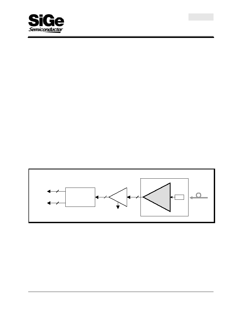
Functional Block Diagram
VCC or +ve supply
SE1030
TzAmp
2.5 Gb/s
Tz Amp
Output
Driver
Bandgap
Reference
Integrator
Rectifier
Automatic Gain Control
TZ_IN
Input
Current
OUTP
OUTN
50
50
R
f
SE1030W
LightCharger
TM
2.5 Gb/s Transimpedance Amplifier
Final
43-DST-01
ß
Rev 1.5
ß
May 24/02
2 of 9
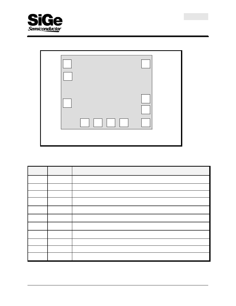
Bondpad Diagram
Top
View
VCC
VCC
VEE2
VEE1
VEE1
VEE1
TZ_IN
OUTN
OUTP
VCC
11
10
9
7
6
5
4
3
8
1
2
DNC
Bondpad Description
Pad No.
Name
Description
1
VCC
Positive supply (+3.3 V), pads 1, 8 & 11 are connected on chip. Only one pad needs
to be bonded.
2
DNC
Do not connect.
3
TZ_IN
Input pad (connect to photodetector anode).
4
VEE2
Negative supply (0V) ≠ Note this is separate ground for the input stage, which is AC
coupled on chip. There is no DC current through this pad.
5
VEE1
Negative supply (0V), pads 5, 6 & 7 are connected on chip. Only one pad needs to be
bonded.
6
VEE1
Negative supply (0V), pads 5, 6 & 7 are connected on chip. Only one pad needs to be
bonded.
7
VEE1
Negative supply (0V), pads 5, 6 & 7 are connected on chip. Only one pad needs to be
bonded.
8
VCC
Positive supply (+3.3 V), pads 1, 8 & 11 are connected on chip. Only one pad needs
to be bonded.
9
OUTN
Negative differential voltage output.
10
OUTP
Positive differential voltage output.
11
VCC
Positive supply (+3.3 V), pads 1, 8 & 11 are connected on chip. Only one pad needs
to be bonded.
SE1030W
LightCharger
TM
2.5 Gb/s Transimpedance Amplifier
Final
43-DST-01
ß
Rev 1.5
ß
May 24/02
3 of 9
Functional Description
Amplifier Front-End
The transimpedance front-end amplifies an input
current from a photodetector, at pin TZ_IN, to produce
a differential output voltage with the feedback resistor
Rf determining the level of amplification (see the
functional block diagram on page 1). An automatic
gain control loop varies this resistor, to ensure that
the output from the front-end does not saturate the
output driver stage that follows. This gain control
allows input signals of up to 2.6 mA peak.
The input pin TZ_IN is biased at 1.5 V below the
supply voltage VCC, allowing a photodetector to have
a constant reverse bias by connecting the cathode to
3.3 V. This enables full single rail operation.
The front-end stage has its own supply ground
connection (VEE2) to achieve optimum noise
performance and maintain integrity of the high-speed
signal path. The front-end shares the VCC (+3.3 V)
connection with the remainder of the circuitry, which has
a separate ground (VEE1).
Output driver stage
The output driver acts as a buffer stage, capable of
swinging up to 300 mVpk-pk differential into a 100
load. The small output swings allow ease of use with
low voltage post amplifiers (e.g. 3.3 V parts).
Increasing optical input level gives a positive-going
output signal on the OUTP pin.
Automatic Gain Control (AGC)
The AGC circuit monitors the voltages from the output
driver and compares them to an internal reference
level produced via the on-chip bandgap reference
circuit. When this level is exceeded, the gain of the
front-end is reduced by controlling the feedback
resistor Rf.
A long time-constant integrator is used within the
control loop of the AGC with a typical low frequency
cut-off of 5 kHz.
System Block Diagram
Receiver Module
Clock & Data
Recovery
Clock
Data
2
2
2.5 Gb/s
2.5 GHz
2
PIN
SE1030W
2
TZ
Amplifier
SE1230
AGC
Amplifier
LOS
SE1030W
LightCharger
TM
2.5 Gb/s Transimpedance Amplifier
Final
43-DST-01
ß
Rev 1.5
ß
May 24/02
4 of 9
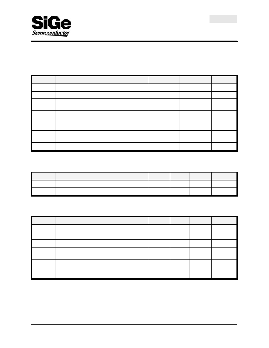
Absolute Maximum Ratings
These are stress ratings only. Exposure to stresses beyond these maximum ratings may cause permanent damage
to, or affect the reliability of the device. Avoid operating the device outside the recommended operating conditions
defined below.
Symbol
Parameter
Min
Max
Unit
VCC
Supply Voltage
≠0.7
6.0
V
V
IO
Voltage at any input or output
≠0.5
VCC+0.5
V
I
IO
Current sourced into any input or output except
TZ_IN
≠20
20
mA
I
IO
Current sourced into pin TZ_IN
≠5
5
mA
V
ESD
Electrostatic Discharge (100 pF, 1.5 k
) except
TZ_IN
≠2
2
kV
V
ESD
Electrostatic Discharge (100 pF, 1.5 k
) pin
TZ_IN
≠0.25
0.25
kV
Tstg
Storage Temperature
≠65
150
∞
C
Recommended Operating Conditions
Symbol
Parameter
Min
Typ
Max
Unit
VCC
Supply Voltage
3.1
3.3
3.5
V
Tj
Operating Junction Temperature
≠40
125
∞
C
DC Electrical Characteristics
Symbol
Parameter
Min
Typ
Max
Unit
ICC max
Supply Current (max input current)
66
101
mA
ICC zero
Supply Current (zero input current)
52
85
mA
lagc
AGC Threshold
42
µ
A pk-pk
Vin
Input Bias Voltage
VCC≠
1.57
VCC≠
1.52
VCC≠
1.47
V
Vout
Output Bias Voltage
VCC≠
0.30
V
Rout
Output Resistance
35
50
65

SE1030W
LightCharger
TM
2.5 Gb/s Transimpedance Amplifier
Final
43-DST-01
ß
Rev 1.5
ß
May 24/02
5 of 9
AC Electrical Characteristics
Symbol
Parameter
Min
Typ
Max
Unit
BW (3dB)
Small Signal Bandwidth at ≠3dB point
1.8
2.4
GHz
Tz
Differential Transimpedance (50
on each output,
f = 100 MHz)
1.6
2.3
3.1
k
Dri
Input Data Rate
50
2500
Mb/s
Voutmax
Maximum Differential Output Voltage
300
mV pk-pk
Flf
Low Frequency Cut-off
5
kHz
l
OL
Input Current before overload (2.5 Gb/s NRZ data)
2600
µ
A pk-pk
Pol
Optical Overload
+1.6
dBm
Nrms
Input Noise Current (in 2 GHz)
360
500
nA rms
DC and AC electrical characteristics are specified under the following conditions:
Supply Voltage (VCC).........................................3.1 V to 3.5 V
Junction Temperature (Tj)..................................≠40
∞
C to 125
∞
C
Load Resistor (R
L
)...............................................50
AC coupled via 220 nF, for each output
Photodetector Capacitance (Cd).......................0.5 pF
Input bond wire inductance................................1 nH
Photodetector responsivity.................................0.9 A/W
Transimpedance (Tz) measured with 4
µ
A mean photocurrent