Document Outline
- S-1111/1121 Series
- Cover
- Features
- Applications
- Packages
- Block Diagram
- Product Code Structure
- Pin Configuration
- Absolute Maximum Ratings
- Electrical Characteristics
- Test Circuits
- Standard Circuit
- Application Conditions
- Explanation of Terms
- Operation
- Selection of Output Capacitor (CL)
- Precautions
- Typical Characteristics
- Rsference Data
- Package Drawings

Rev.2.2
_00
HIGH RIPPLE-REJECTION
LOW DROPOUT CMOS VOLTAGE REGULATOR
S-1111/1121 Series
Seiko Instruments Inc.
1
The S-1111/1121 Series is a positive voltage
regulator with a low dropout voltage, high output
voltage accuracy, and low current consumption
developed based on CMOS technology.
A built-in low on-resistance transistor provides a
low dropout voltage and large output current, and
a built-in overcurrent protector prevents the load
current from exceeding the current capacitance of
the output transistor. An ON/OFF circuit ensures a
long battery life, and small SOT-23-5 and 5-Pin
SON(A) packages realize high-density mounting.
The lineup includes the S-1111 and S-1121
Series, which differ in pin configuration.
Features
� Output voltage:
1.5 V to 5.5 V, selectable in 0.1 V steps.
� High-accuracy output voltage: �1.0%
� Low dropout voltage:
200 mV typ. (3.0 V output product, I
OUT
= 100 mA)
� Low current consumption:
During operation: 35
�A typ., 65 �A max.
During shutdown: 0.1
�A typ., 1.0 �A max.
� High peak current capability:
150 mA output is possible (@ V
IN
V
OUT(S)
+ 1.0 V)
*1
� Built-in ON/OFF circuit:
Ensures long battery life.
� High ripple rejection:
70 dB typ. (@ 1.0 kHz)
� Built-in overcurrent protector: Overcurrent of output transistor can be restricted.
� Small package:
SOT-23-5, 5-Pin SON(A)
*1. Attention should be paid to the power dissipation of the package when the output current is large.
Applications
� Power supply for battery-powered devices
� Power supply for personal communication devices
� Power supply for home electric/electronic appliances
� Power supply for cellular phones
Packages
� SOT-23-5
(Package drawing code: MP005-A)
� 5-Pin SON(A)
(Package drawing code: PN005-A)

HIGH RIPPLE-REJECTION LOW DROPOUT CMOS VOLTAGE REGULATOR
S-1111/1121 Series
Rev.2.2
_00
2
Seiko Instruments Inc.
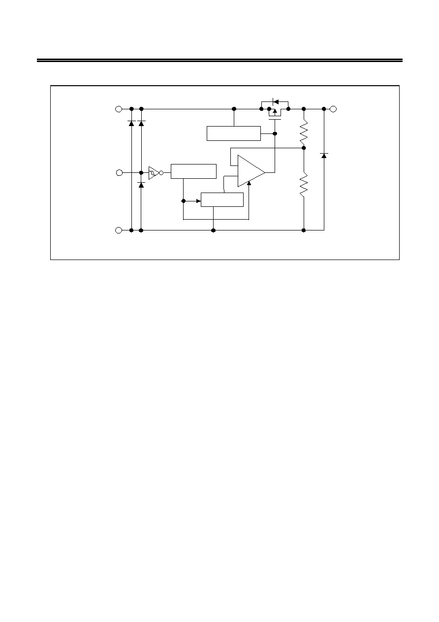
Block Diagram
VIN
VSS
VOUT
Overcurrent
protector
Reference
voltage circuit
ON/OFF
*1. Parasitic diode
*1
ON/OFF
circuit
+
-
Figure 1

HIGH RIPPLE-REJECTION LOW DROPOUT CMOS VOLTAGE REGULATOR
Rev.2.2
_00
S-1111/1121 Series
Seiko Instruments Inc.
3
Product Code Structure
� The product types and output voltage for the S-1111/1121 Series can be selected at the user's request.
Refer to the "Product name" for the meanings of the characters in the product name and "Product name
list" for the full product names.
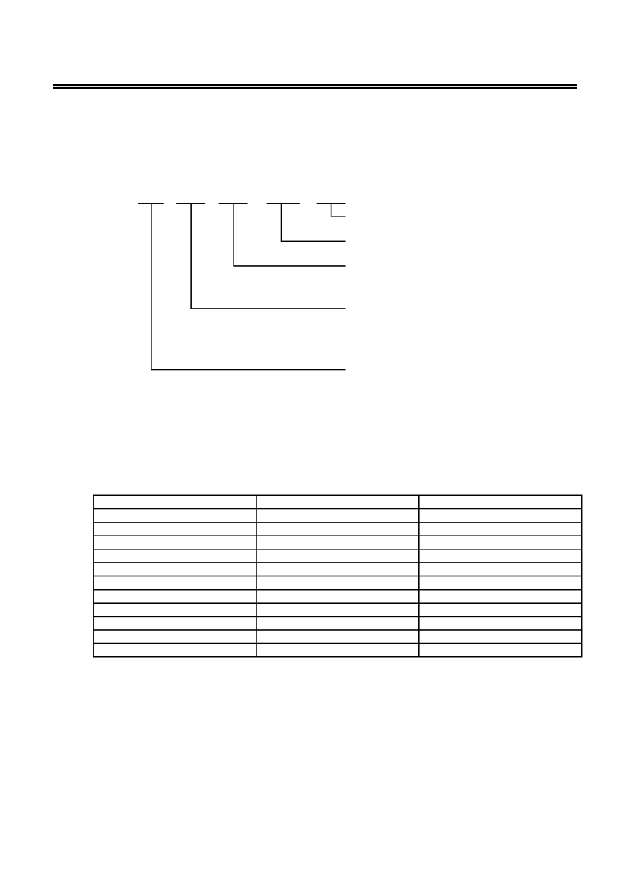
1. Product name (S-1111 Series)
S-1111
x xx xx � xxx
� TF
IC direction in tape specifications
*1
Product name (abbreviation)
*2
Package name (abbreviation)
MC:
SOT-23-5
PN: 5-Pin SON(A)
Output voltage
15 to 55
(E.g., when the output voltage is 1.5 V, it is
expressed as 15.)
Product type
*3
A: ON/OFF pin negative logic
B: ON/OFF pin positive logic
*1. Refer to the taping specifications at the end of this book.
*2. Refer to the product name list.
*3. Refer to 3. Shutdown (ON/OFF pin) under the Operation.
2. Product name list (S-1111 Series)
Table 1
Output Voltage
SOT-23-5
5-Pin SON(A)
1.5 V �1.0%
S-1111B15MC-NYA-TF
S-1111B15PN-NYA-TF
1.8 V �1.0%
S-1111B18MC-NYD-TF
S-1111B18PN-NYD-TF
2.5 V �1.0%
S-1111B25MC-NYK-TF
S-1111B25PN-NYK-TF
2.6 V �1.0%
S-1111B26MC-NYL-TF
S-1111B26PN-NYL-TF
2.7 V �1.0%
S-1111B27MC-NYM-TF
S-1111B27PN-NYM-TF
2.8 V �1.0%
S-1111B28MC-NYN-TF
S-1111B28PN-NYN-TF
2.9 V �1.0%
S-1111B29MC-NYO-TF
S-1111B29PN-NYO-TF
3.0 V �1.0%
S-1111B30MC-NYP-TF
S-1111B30PN-NYP-TF
3.1 V �1.0%
S-1111B31MC-NYQ-TF
S-1111B31PN-NYQ-TF
3.3 V �1.0%
S-1111B33MC-NYS-TF
S-1111B33PN-NYS-TF
5.0 V �1.0%
S-1111B50MC-NZJ-TF
S-1111B50PN-NZJ-TF
Remark Please contact the SII marketing department for products with an output voltage other than
those specified above or type A products.

HIGH RIPPLE-REJECTION LOW DROPOUT CMOS VOLTAGE REGULATOR
S-1111/1121 Series
Rev.2.2
_00
4
Seiko Instruments Inc.
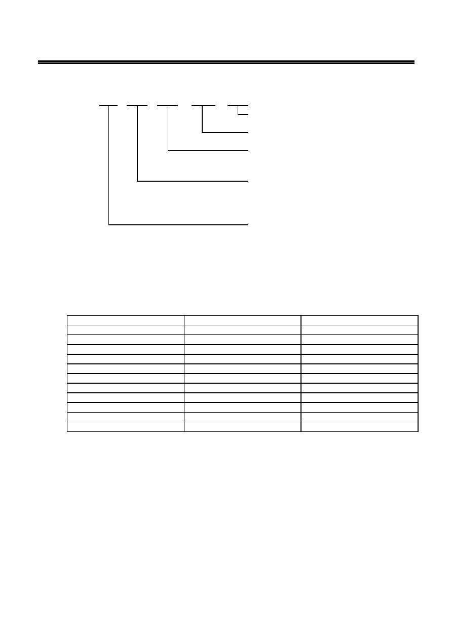
3. Product name (S-1121 Series)
S-1121
x xx xx � xxx � TF
IC direction in tape specifications
*1
Product name (abbreviation)
*2
Package name (abbreviation)
MC:
SOT-23-5
PN: 5-Pin SON(A)
Output voltage
15 to 55
(E.g., when the output voltage is 1.5 V, it is
expressed as 15.)
Product type
*3
A: ON/OFF pin negative logic
B: ON/OFF pin positive logic
*1. Refer to the taping specifications at the end of this book.
*2. Refer to the product name list.
*3. Refer to 3. Shutdown pin (ON/OFF pin) under the Operation.
4. Product name list (S-1121 Series)
Table 2
Output Voltage
SOT-23-5
5-Pin SON(A)
1.5 V �1.0%
S-1121B15MC-N2A-TF
S-1121B15PN-N2A-TF
1.8 V �1.0%
S-1121B18MC-N2D-TF
S-1121B18PN-N2D-TF
2.5 V �1.0%
S-1121B25MC-N2K-TF
S-1121B25PN-N2K-TF
2.6 V �1.0%
S-1121B26MC-N2L-TF
S-1121B26PN-N2L-TF
2.7 V �1.0%
S-1121B27MC-N2M-TF
S-1121B27PN-N2M-TF
2.8 V �1.0%
S-1121B28MC-N2N-TF
S-1121B28PN-N2N-TF
2.9 V �1.0%
S-1121B29MC-N2O-TF
S-1121B29PN-N2O-TF
3.0 V �1.0%
S-1121B30MC-N2P-TF
S-1121B30PN-N2P-TF
3.1 V �1.0%
S-1121B31MC-N2Q-TF
S-1121B31PN-N2Q-TF
3.3 V �1.0%
S-1121B33MC-N2S-TF
S-1121B33PN-N2S-TF
5.0 V �1.0%
S-1121B50MC-N3J-TF
S-1121B50PN-N3J-TF
Remark Please contact the SII marketing department for products with an output voltage other than
those specified above or type A products.

HIGH RIPPLE-REJECTION LOW DROPOUT CMOS VOLTAGE REGULATOR
Rev.2.2
_00
S-1111/1121 Series
Seiko Instruments Inc.
5
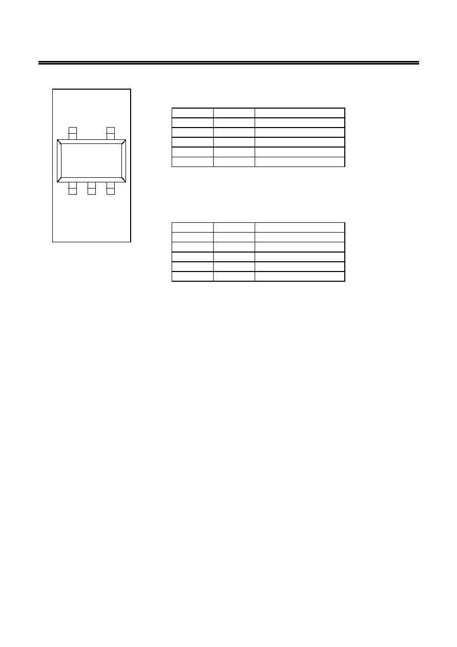
Pin Configuration
Table 3
(S-1111
Series)
Pin
No.
Symbol
Description
1
VIN
Input voltage pin
2
VSS
GND
pin
3
ON/OFF
Shutdown
pin
4
NC
*1
No connection
5
VOUT
Output voltage pin
*1. The NC pin is electrically open.
The NC pin can be connected to VIN or VSS.
Table 4
(S-1121
Series)
Pin No.
Symbol
Description
5 4
1 3
2
SOT-23-5
Top view
1
VOUT
Output voltage pin
2
VSS GND
pin
Figure 2
3
VIN
Input voltage pin
4
ON/OFF
Shutdown
pin
5
NC
*1
No connection
*1. The NC pin is electrically open.
The NC pin can be connected to VIN or VSS.

